

Page 1
SERVICE MANUAL
DL3103DC
Page 2

CONTENTS
1. SAFETY PRECAUTIONS
1
2. PREVE NTION OF ELE CTR O STATIC DISCHARGE(ESD)TO ELECTROSTATICALLY
SENS ITIVE(ES)DEVICES
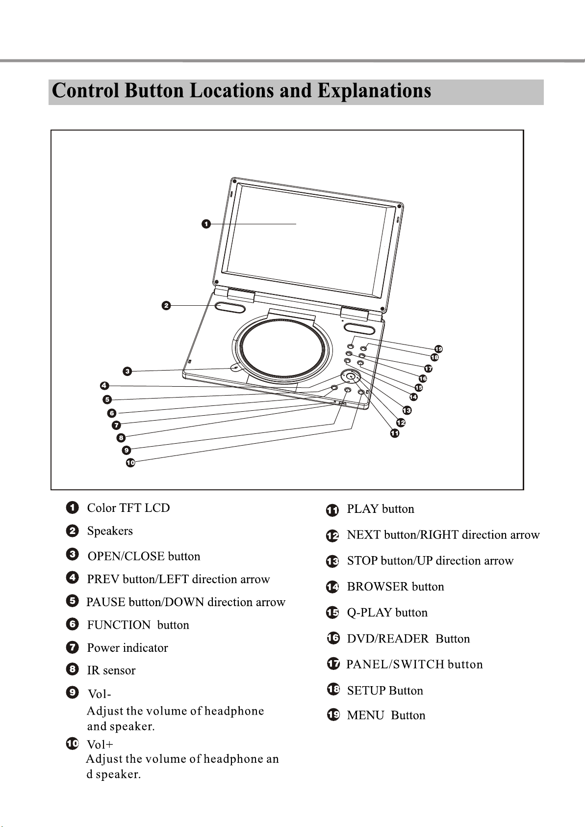
3. CONTROL BUTTON LOCATIONS AND E XPLANATIONS
4. PREVE RTION OF STATIC ELE CTRICITY DISCHARGE
5. E LE C TR IC AL C ONFIR MATION
5.1 VIDE O OUTP UT (LUMINANC E S IG NAL) C ONFIR MATION
5.2 VIDE O OUTP UT(C HR OMINANC E S IG NAL) C ONFIR MATION
6. MP E G BOAR D C HE C K WAVE FOR M
7.2 MT1389
1
2
4
5
5
6
7
8
7.3 HY29LV160 11
7.4 HY57V641620HG
14
8. S C HE MATIC & P C B WIR ING DIAG R AM
17
9. S P AR E P AR TS LIS T 33
Page 3

1.1 GENERAL GUIDELINES
1. SAFETY PREAUTIONS
2.PREVENTION OF ELECTRO STATIC DISCHARGE(ESD)TO
ELECTROSTATICALLY SENSITIVE(ES)DEVICES
1
1. When servicing, observe the original lead dress. if a short circuit is found, replace all parts which have
been overheated or damaged by the short circuit.
2. After servicing, see to it that all the protective devices such as insulation barrier, insulation papers
shields are properly installed.
3. After servicing, make the following leakage current checks to prevent the customer from being exposed
to shock hazards.
Some semiconductor(solid state)devices can be damaged easily by static electricity. Such components
commonly are called Electrostatically Sensitive(ES)Devices. Examples of typical ES devices are integrated
circuits and some field-effect transistors and semiconductor chip components. The following techniques
should be used to help reduce the incidence of component damage caused by electro static discharge(ESD).
1. Immediately before handling any semiconductor component or semiconductor-equipped assembly, drain
off any ESD on your body by touching a known earth ground. Alternatively, obtain and wear a commercially
availabel discharging ESD wrist strap, which should be removed for potential shock reasons prior to
applying power to the unit under test.
2. After removing an electrical assembly equipped with ES devices,place the assembly on a conductive
surface such as alminum foil, to prevent electrostatic charge buildup or exposure of the assembly.
3. Use only a grounded-tip soldering iron to solder or unsolder ES devices.
4. Use only an anti-static solder removal device. Some solder removal devices not classified as anti-static
(ESD protected)can generate electrical charge sufficient to damage ES devices.
5. Do not use freon-propelled chemicals. These can generate electrical charges sufficient to damage ES
devices.
6. Do not remove a replacement ES device from its protective package until immediately before you are
ready to install it. (Most replacement ES devices are packaged with leads electrically shorted together by
conductive foam, alminum foil or comparable conductive material).
7. Immediately before removing the protective material from the leads of a replacement ES device, touch
the protective material to the chassis or circuit assembly into which the device will be installed.
Caution
Be sure no power is applied to the chassis or circuit, and observe all other safety precautions.
8. Minimize bodily motions when handling unpackaged replacement ES devices. (Otherwise harmless motion
such as the brushing together of your clothes fabric or the lifting of your foot from a carpeted floor can
generate static electricity(ESD).
notice (1885x323x2 tiff)
Page 4
2
Page 5
3
Page 6
The laser diode in the traverse unit (optical pickup)may brake down due to static electricity of clothes or human
body. Use due caution to electrostatic breakdown when servicing and handling the laser diode.
Some devices such as the DVD player use the optical pickup(laser diode)and the optical pickup will be damaged
by static electricity in the working environment.Proceed servicing works under the working environment where
1. Put a conductive material(sheet)or iron sheet on the area where the optical pickup is placed,and ground the
3. The flexible cable may be cut off if an excessive force is applied to it.Use caution when handling the cable.
4
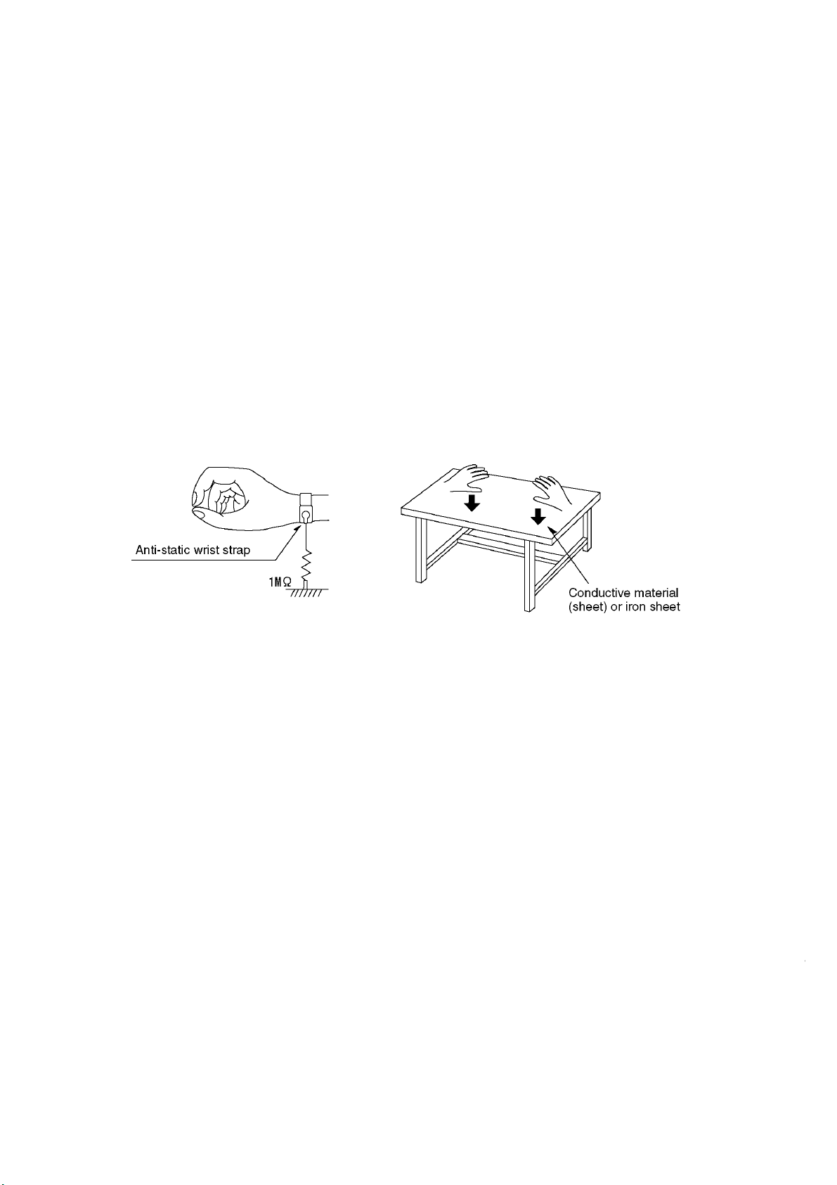
4.PREVENTION OF STATIC ELECTRICITY DISCHARGE
4.1.Grounding for electrostatic breakdown prevention
grounding works is completed.
4.1.1. Worktable grounding
sheet.
4.1.2.Human body grounding
1 Use the anti-static wrist strap to discharge the static electricity from your body.
safety_3 (1577x409x2 tiff)
4.1.3.Handling of optical pickup
1. To keep the good quality of the optical pickup maintenance parts during transportation and before
installation, the both ends of the laser diode are short-circuited.After replacing the parts with new ones,
remove the short circuit according to the correct procedure. (See this Technical Guide).
2. Do not use a tester to check the laser diode for the optical pickup .Failure to do so willdamage the laser
diode due to the power supply in the tester.
4.2. Handling precautions for Traverse Unit (Optical Pickup)
1. Do not give a considerable shock to the traverse unit(optical pickup)as it has an extremely high-precise
structure.
2. When replacing the optical pickup, install the flexible cable and cut is short land with a nipper. See the
optical pickup replacement procedure in this Technical Guide. Before replacing the traverse unit, remove
the short pin for preventingstatic electricity and install a new unit.Connect the connector as short times as
possible.
4. The half-fixed resistor for laser power adjustment cannot be adjusted. Do not turn the resistor.
Page 7
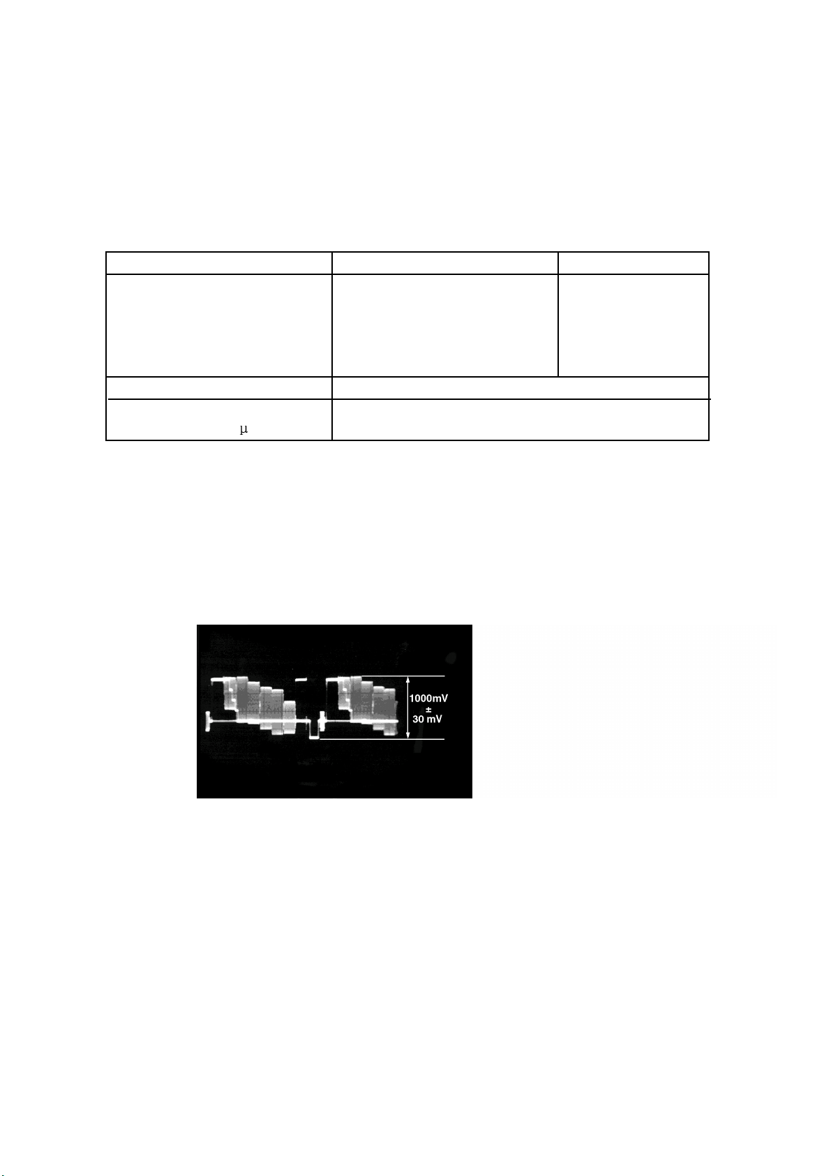
5.1. Video Output (Luminance Signal) Confirmation
5
5.Electrical Confirmation
DO this confirmation after replacing a P.C.B.
Measurement point
Video output terminal
Measuring equipment,tools
200mV/dir,10 sec/dir
Purpose:To maintain video signal output compatibility.
1.Connect the oscilloscope to the video output terminal and terminate at 75 ohms.
2.Confirm that luminance signal(Y+S)level is 1000mVp-p±30mV
PLAY(Title 46):DVDT-S15
PLAY(Title 12):DVDT-S01
Mode Disc
Color bar 75%
Confirmation value
1000mVp-p±30mV
DVDT-S15
or
DVDT-S01
Page 8
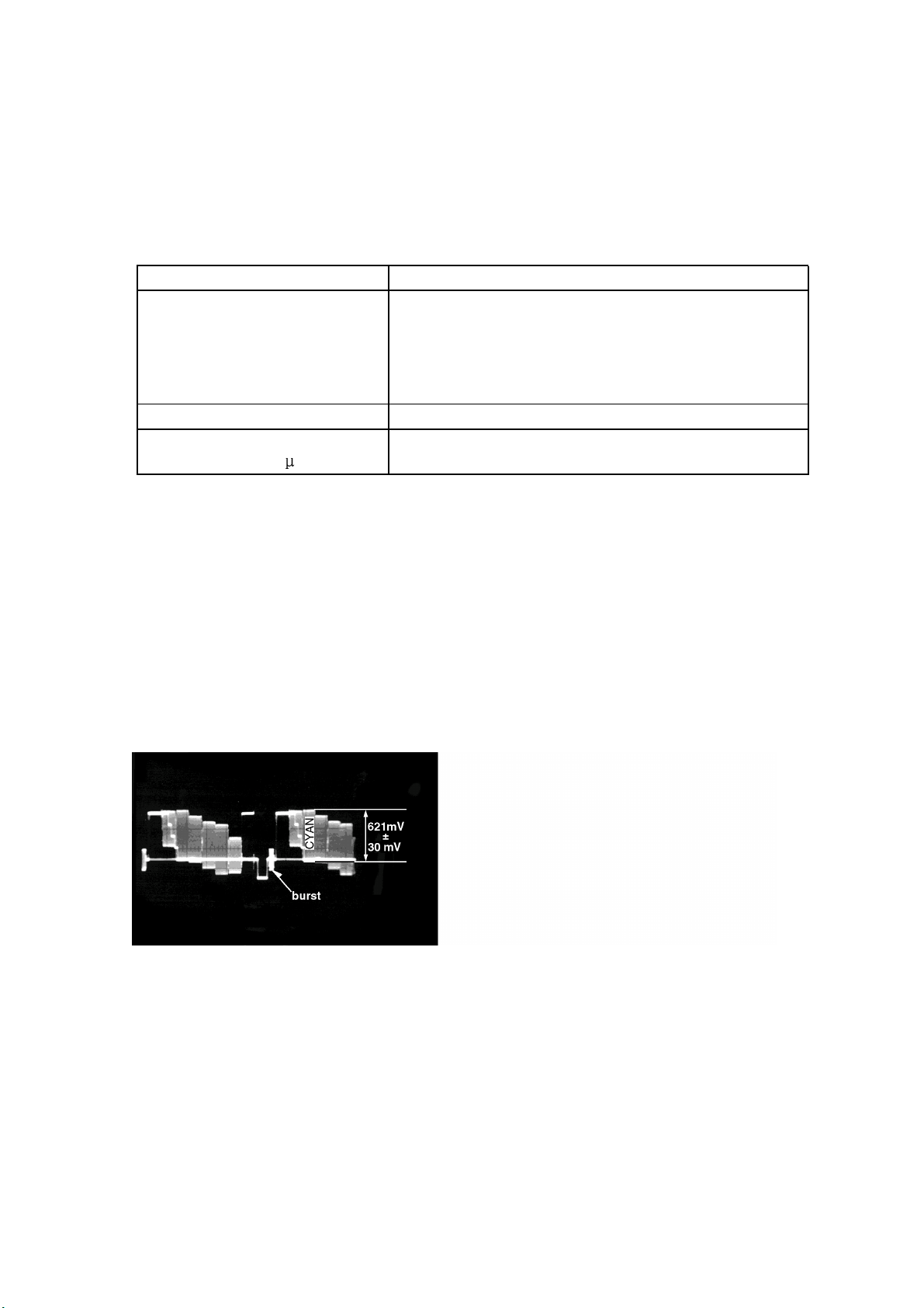
Do the confirmation after replacing P.C.B.
Screwdriver,Oscilloscope
5.2 Video Output(Chrominance Signal) Confirmation
6
Measurement point
Video output terminal
Measuring equipment,tools Confirmation value
200mV/dir,10 sec/dir
Purpose:To maintain video signal output compatibility.
1.Connect the oscilloscope to the video output terminal and terminate at 75 ohme.
2.Confirm that the chrominance signal(C)level is 621 mVp-p±30mV
PLAY(Title 46):DVDT-S15
PLAY(Title 12):DVDT-S01
Mode Disc
Color bar 75%
621mVp-p±30mV
DVDT-S15
or
DVDT-S01
Page 9
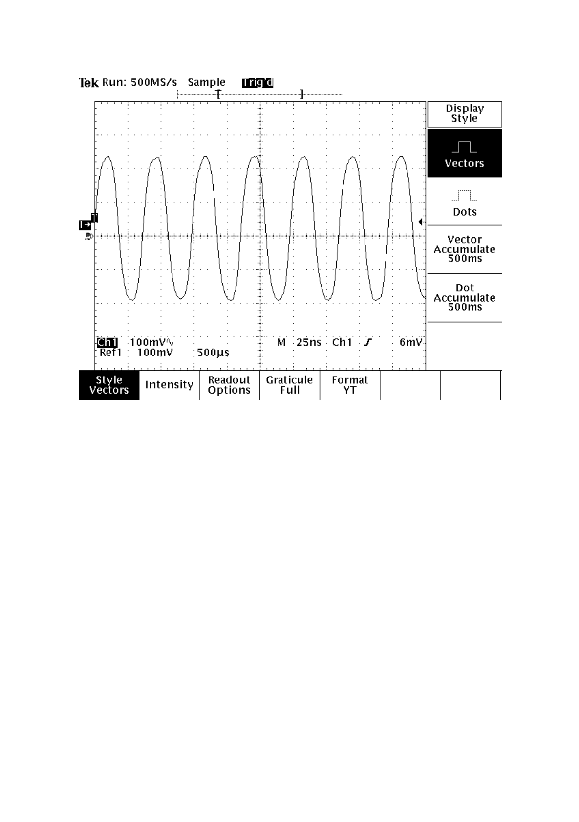
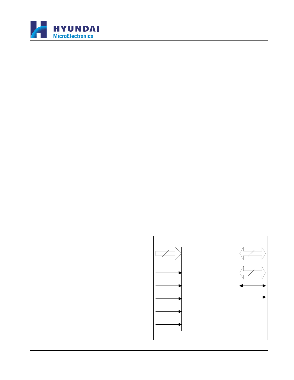
6.MPEG BOARD CHECK WAVEFORM
6.1 27MHz WAVEFORM
7
Page 10
7.2 MT1389
8
MT1389
Specifications are subject to change without notice
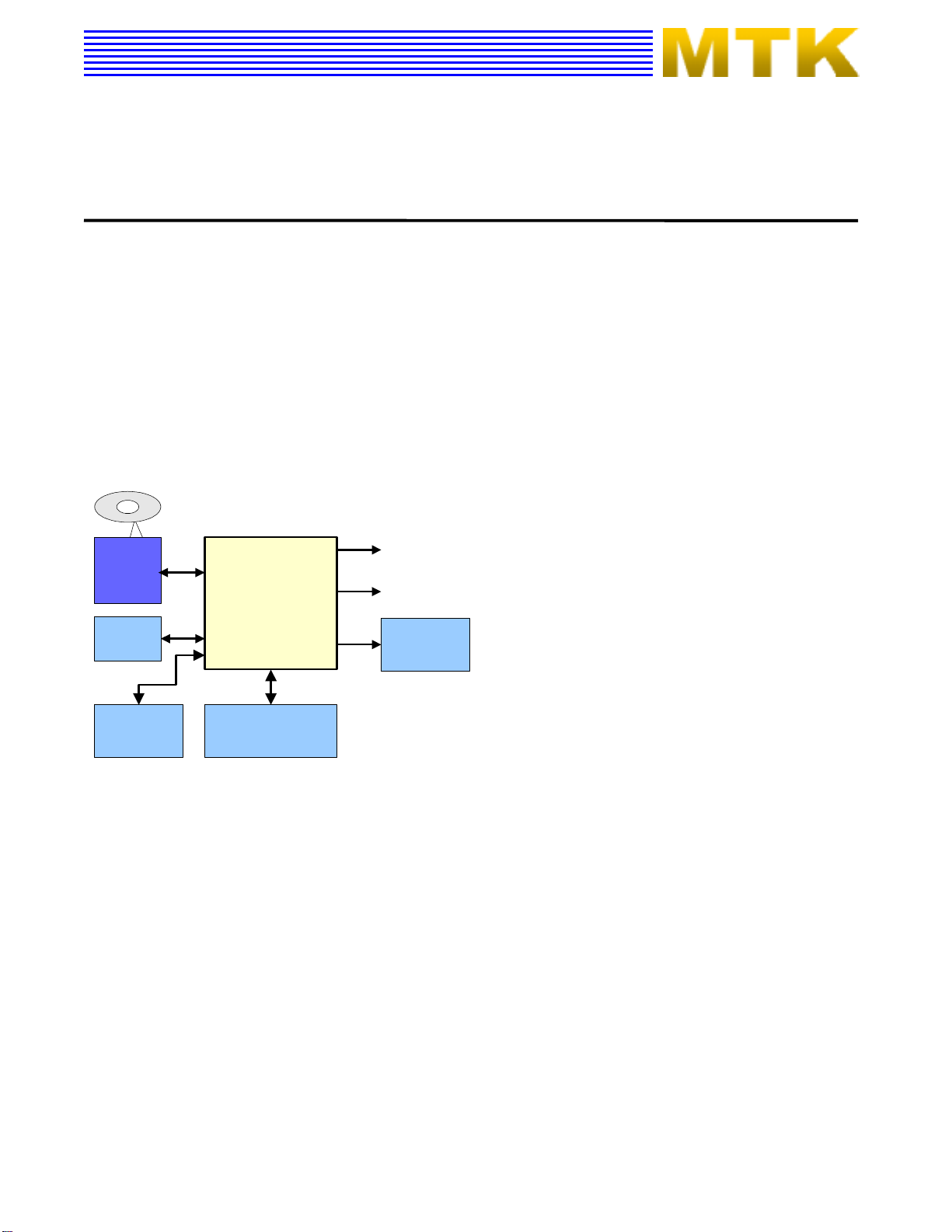
Progressive-Scan DVD Player SOC
MediaTek MT1389 is a DVD player system-on-chip (SOC) which incorporates advanced features like high
quality TV encoder and state-of-art de-interlace processing. The MT1389 enables consumer electronics
manufacturers to build high quality, cost-effective DVD players, portable DVD players or any other home
entertainment audio/video devices.
rd
Based on MediaTek’s world-leading DVD player SOC architecture, the MT1389 is the 3
player SOC. It integrates the MediaTek 2
decoder.
The progressive scan of the MT1389 utilized a proprietary advanced motion-adaptive de-interlace algorithm to
achieve the best movie/video playback. It can easily detect 3:2/2:2 pull down source and restore the correct
original pictures. It also supports a patent-pending edge-preserving algorithm to remove the saw-tooth effect.
nd
generation front-end analog RF amplifier and the Servo/MPEG AV
generation of the DVD
Key Features
RF/Servo/MPEG Integration
High Performance Audio Processor
Motion-Adaptive, Edge-Preserving De-interlace
108MHz/12-bit, 6 CH TV Encoder
DVD
PUH
Module
CVBS, Y/C,
Component
SDPIF
MT1389L
Applications
FLASH
Front-panel
Remote
DRAM
Audio DAC
Standard DVD Players
Portable DVD Players
DVD Player System Diagram Using MT1389
Page 11

9
PRELIMINARY, SUBJECT TO CHANGE WITHOUT NOTICE MTK CONFIDENTIAL, NO DISCLOSURE
MT1389
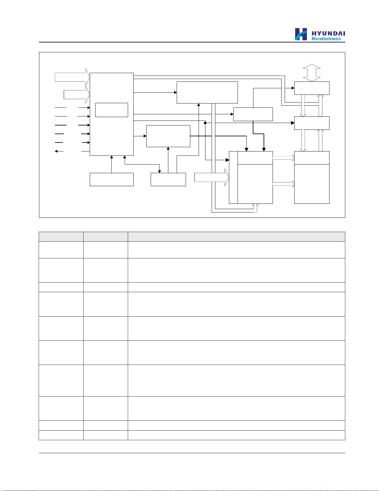
General Feature List
1024-bytes on-chip RAM
Super Integration DVD player single chip
High performance analog RF amplifier
Servo controller and data channel processing
MPEG-1/MPEG-2/JPEG video
Dolby AC-3/DTS/DVD-Audio
Unified memory architecture
Versatile video scaling & quality
enhancement
OSD & Sub-picture
2-D graphic engine
Built-in clock generator
Built-in high quality TV encoder
Built-in progressive video processor
Audio effect post-processor
Audio input port
Up to 4M bytes FLASH-programming
interface
Supports 5/3.3-Volt. FLASH interface
Supports power-down mode
Supports additional serial port
DVD-ROM/CD-ROM Decoding Logic
High-speed ECC logic capable of correcting
one error per each P-codeword or
Q-codeword
Automatic sector Mode and Form detection
Automatic sector Header verification
Decoder Error Notification Interrupt that
signals various decoder errors
Provide error correction acceleration
High Performance Analog RF Amplifier
Programmable fc
Dual automatic laser power control
Defect and blank detection
RF level signal generator
Speed Performance on Servo/Channel Decoding
DVD-ROM up to 4XS
CD-ROM up to 24XS
Channel Data Processor
Digital data slicer for small jitter capability
Built-in high performance data PLL for
channel data demodulation
EFM/EFM+ data demodulation
Enhanced channel data frame sync protection
& DVD-ROM sector sync protection
Servo Control and Spindle Motor Control
Programmable frequency error gain and
phase error gain of spindle PLL to control
spindle motor on CLV and CAV mode
Built-in ADCs and DACs for digital servo
control
Provide 2 general PWM
Tray control can be PWM output or digital
output
Embedded Micro controller
Built-in 8032 micro controller
Built-in internal 373 and 8-bit programmable
lower address port
Buffer Memory Controller
Supports 16Mb/32Mb/64Mb/128Mb SDRAM
Supports 16-bit SDRAM data bus
Provide the self-refresh mode SDRAM
Block-based sector addressing
Support 3.3 Volt. DRAM Interface
Video Decode
Decodes MPEG1 video and MPEG2 main level,
main profile video (720/480 and 720x576)
Smooth digest view function with I, P and B
picture decoding
Baseline, extended-sequential and
progressive JPEG image decoding
Support CD-G titles
Video/OSD/SPU/HLI Processor
Arbitrary ratio vertical/horizontal scaling of
video, from 0.25X to 256X
65535/256/16/4/2-color bitmap format OSD,
256/16 color RLC format OSD
Automatic scrolling of OSD image
Slide show transition as DVD-Audio
Specification
2-D Graphic Engine
Support decode Text and Bitmap
Support line, rectangle and gradient fill
Support bitblt
Chroma key copy operation
Clip mask
Page 12

10
PRELIMINARY, SUBJECT TO CHANGE WITHOUT NOTICE MTK CONFIDENTIAL, NO DISCLOSURE
MT1389
Audio Effect Processing
Dolby Digital (AC-3)/EX decoding
DTS/DTS-ES decoding
MLP decoding for DVD-Audio
MPEG-1 layer 1/layer 2 audio decoding
MPEG-2 layer1/layer2 2-channel audio
High Definition Compatible Digital (HDCD)
Windows Media Audio (WMA)
Advanced Audio Coding (AAC)
Dolby ProLogic II
Concurrent multi-channel and downmix out
IEC 60958/61937 output
- PCM / bit stream / mute mode
- Custom IEC latency up to 2 frames
Pink noise and white noise generator
Karaoke functions
- Microphone echo
- Microphone tone control
- Vocal mute/vocal assistant
- Key shift up to +/- 8 keys
- Chorus/Flanger/Harmony/Reverb
Channel equalizer
3D surround processing include virtual
surround and speaker separation
TV Encoder
Six 108MHz/12bit DACs
Support NTSC, PAL-BDGHINM, PAL-60
Support 525p, 625p progressive TV format
Automatically turn off unconnected channels
Support PC monitor (VGA)
Support Macrovision 7.1 L1, Macrovision
525P and 625P
CGMS-A/WSS
Closed Caption
Progressive Output
Automatic detect film or video source
3:2 pull down source detection
Advanced Motion adaptive de-interlace
Edge Preserving
Minimum external memory requirement
Audio Input
Line-in/SPDIF-in for versatile audio
processing
Outline
256-pin LQFP package
3.3/1.8-Volt. Dual operating voltages
Page 13
KEY FEATURES
IC BLOCK DIAGRAM & DESCRIPTION
11
HY29LV160
16 Mbit (2M x 8/1M x 16) Low Voltage Flash Memory
nn
n Single Power Supply Operation
nn
– Read, program and erase operations from
2.7 to 3.6 volts
– Ideal for battery-powered applications
nn
n High Performance
nn
– 70, 80, 90 and 120 ns access time
versions
nn
n Ultra-low Power Consumption (Typical
nn
Values At 5 Mhz)
– Automatic sleep mode current: 1 µA
– Standby mode current: 1 µA
– Read current: 9 mA
– Program/erase current: 20 mA
nn
n Flexible Sector Architecture:
nn
– One 16 KB, two 8 KB, one 32 KB and
thirty-one 64 KB sectors in byte mode
– One 8 KW, two 4 KW, one 16 KW and
thirty-one 32 KW sectors in word mode
– Top or bottom boot block configurations
available
nn
n Sector Protection
nn
– Allows locking of a sector or sectors to
prevent program or erase operations
within that sector
– Sectors lockable in-system or via
programming equipment
– Temporary Sector Unprotect allows
changes in locked sectors (requires high
voltage on RESET# pin)
nn
n Fast Program and Erase Times
nn
– Sector erase time: 0.25 sec typical for
each sector
– Chip erase time: 8 sec typical
– Byte program time: 9 µs typical
nn
n Unlock Bypass Program Command
nn
– Reduces programming time when issuing
multiple program command sequences
nn
n Automatic Erase Algorithm Preprograms
nn
and Erases Any Combination of Sectors
or the Entire Chip
nn
n Erase Suspend/Erase Resume
nn
– Suspends an erase operation to allow
reading data from, or programming data
to, a sector that is not being erased
– Erase Resume can then be invoked to
complete suspended erasure
nn
n Automatic Program Algorithm Writes and
nn
Verifies Data at Specified Addresses
nn
n 100,000 Write Cycles per Sector Minimum
nn
nn
n Data# Polling and Toggle Bits
nn
– Provide software confirmation of
completion of program and erase
operations
nn
n Ready/Busy# Pin
nn
– Provides hardware confirmation of
completion of program and erase
operations
nn
n Hardware Reset Pin (RESET#) Resets the
nn
Device to Reading Array Data
nn
n Compliant With Common Flash Memory
nn
Interface (CFI) Specification
– Flash device parameters stored directly
on the device
– Allows software driver to identify and use
a variety of different current and future
Flash products
nn
n Compatible With JEDEC standards
nn
– Pinout and software compatible with
single-power supply Flash devices
– Superior inadvertent write protection
nn
n Space Efficient Packaging
nn
– 48-pin TSOP and 48-ball FBGA packages
LOGIC DIAGRAM
20
A[19:0]
CE#
OE#
WE#
RESET#
BYTE#
DQ[7:0]
DQ[14:8]
DQ15/A-1
RY/BY#
8
7
Preliminary
Revision 1.0, June 2000
Page 14
HY29LV160
IC BLOCK DIAGRAM & DESCRIPTION
12
BLOCK DIAGRAM
DQ[15:0]
A[19:0], A-1
DQ[15:0]
WE#
CE#
OE#
BYTE#
RESET#
RY/BY#
STATE
CONTROL
COMMAND
REGISTER
VCC DETECTOR TIMER
SIGNAL DESCRIPTIONS
emaN epyT noitpircseD
]0:91[AstupnI
,]1-[A/]51[QD
]0:41[QD
#ETYBtupnI
#ECtupnI
#EOtupnI
#EWtupnI
#TESERtupnI
#YB/YR
V
CC
V
SS
--
--
ERASE VOLTAGE
GENERATOR AND
SECTOR SWITCHES
I/O CONTROL
PROGRAM
VOLTAGE
GENERATOR
Y-DECODER
A[19:0], A-1
X-DECODER
ADDRESS LATCH
I/O BUFFERS
DATA LATCH
Y-GATING
16 Mb FLASH
MEMORY
ARRAY
.hgiHevitca,sserddA nitupni]1-[A/]51[QDehthtiwdenibmoc,stupni02esehT
.snoitarepoetirwrodaerrofyarraehtnihtiwnoitacolenotceles,edometyB
stuptuO/stupnI
etats-irT
hgiHevitca,suBataD daerrofhtapatadtib-61ro-8naedivorpsnipesehT.
tib-12ehtfoBSLehtsadesusi]1-[A/]51[QD,edometyBnI.snoitarepoetirwdna
.edometyBnidetats-irtniamerdnadesunuera]8:41[QD.tupnisserddaetyb
.woLevitca,edoMetyB .edomdroWstceleshgiH,edometyBstceleswoL
.woLevitca,elbanEpihC romorfataddaerotdetressaebtsumtupnisihT
ehtdnadetats-irtsisubatadeht,hgiHnehW.061VL92YHehtotatadetirw
.edomybdnatSehtnidecalpsiecived
woLevitca,elbanEtuptuO rofdetagendnasnoitarepodaerrofdetressA.
gniruddaersidrowaroetybarehtehwsenimreted#ETYB.snoitarepoetirw
.noitarepodaereht
.woLevitca,elbanEetirW secneuqesdnammocrosdnammocfognitirwslortnoC
noitarepoetirwA.yarrayromemehtfosrotcesesareroatadmargorpotredroni
hgiHsi#EOdnawoLsi#ECelihwdetressasi#EWnehwecalpsekat.
.woLevitca,teseRerawdraH ehtgnitteserfodohtemerawdrahasedivorP
yletaidemmiti,tesersiecivedehtnehW.etatsyarradaerehtot061VL92YH
ecivedeht,detressasi#TESERelihW.ssergorpninoitarepoynasetanimret
.edomybdnatSehtnieblliw
tuptuO
niarDnepO
.sutatSysuB/ydaeR nisidnammocesareroetirwarehtehwsetacidnI
ylevitcasiecivedehtelihwwoLsniameR.detelpmocneebsahrossergorp
.atadyarradaerotydaersitinehwhgiHseogdna,gnisareroatadgnimmargorp
.ylppusrewop)lanimon(tlov-3
.dnuorglangisdnarewoP
Rev. 1.0/Jun 00
3
Page 15

PIN CONFIGURATIONS
IC BLOCK DIAGRAM & DESCRIPTION
13
HY29LV160
48-Ball FBGA (Bottom View)
A6 B6 C6 D6 E6 F6 G6
A[13] A[12] A[14] A[15] A[16] BYTE# DQ[15]/A[-1] V
A5 B5 C5 D5 E5 F5 G5 H5
A[9] A[8] A[10] A[11] DQ[7] DQ[14] DQ[13] DQ[6]
A4 B4 C4
WE# RESET# NC A[19] DQ[5] DQ[12] V
A3 B3 C3
RY/BY# NC A[18] NC DQ[2] DQ[10] DQ[11] DQ[3]
A2 B2 C2 D2 E2 F2 G2 H2
A[7] A[17] A[6] A[5] DQ[0] DQ[8] DQ[9] DQ[1]
A1 B1 C1 D1 E1 F1 G1
A[3] A[4] A[2] A[1] A[0] CE# OE# V
A[15]
A[14]
A[13]
A[12]
A[11]
A[10]
A[9]
A[8]
A[19]
NC
10
WE#
RESET#1112
NC
NC
RY/BY#
A[18]
A[17]
A[7]
A[6]
A[5]
A[4]
A[3]
A[2]
A[1]
13
14
15
16
17
18
19
20
21
22
23
24
H6
SS
D4
D3
1
2
3
4
5
6
7
8
9
Standard
TSOP48
E4 F4 G4 H4
DQ[4]
CC
E3 F3 G3 H3
H1
SS
48
47
46
45
44
43
42
41
40
39
38
37
36
35
34
33
32
31
30
29
28
27
26
25
A[16]
BYTE#
V
SS
DQ[15]/A[-1]
DQ[7]
DQ[14]
DQ[6]
DQ[13]
DQ[5]
DQ[12]
DQ[4]
V
CC
DQ[11]
DQ[3]
DQ[10]
DQ[2]
DQ[9]
DQ[1]
DQ[8]
DQ[0]
OE#
V
SS
CE#
A[0]
4
Rev. 1.0/Jun 00
Page 16

HY57V641620HG
14
7.4 HY57V641620HG
4 Banks x 1M x 16Bit Synchronous DRAM
DESCRIPTION
The Hyundai HY57V641620HG is a 67,108,864-bit CMOS Synchronous DRAM, ideally suited for the main memory applications which
require large memory density and high bandwidth. HY57V641620HG is organized as 4banks of 1,048,576x16.
HY57V641620HG is offering fully synchronous operation referenced to a positive edge of the clock. All inputs and outputs are synchronized with the rising edge of the clock input. The data paths are internally pipelined to achieve very high bandwidth. All input and output
voltage levels are compatible with LVTTL.
Programmable options include the length of pipeline (Read latency of 2 or 3), the number of consecutive read or write cycles initiated
by a single control command (Burst length of 1,2,4,8 or Full page), and the burst count sequence(sequential or interleave). A burst of
read or write cycles in progress can be terminated by a burst terminate command or can be interrupted and replaced by a new burst
read or write command on any cycle. (This pipelined design is not restricted by a `2N` rule.)
FEATURES
• Single 3.3±0.3V power supply
• All device pins are compatible with LVTTL interface
• JEDEC standard 400mil 54pin TSOP-II with 0.8mm
of pin pitch
• All inputs and outputs referenced to positive edge of
system clock
• Data mask function by UDQM or LDQM
• Internal four banks operation
Note)
• Auto refresh and self refresh
• 4096 refresh cycles / 64ms
• Programmable Burst Length and Burst Type
- 1, 2, 4, 8 or Full page for Sequential Burst
- 1, 2, 4 or 8 for Interleave Burst
• Programmable CAS Latency ; 2, 3 Clocks
.
Page 17

PIN CONFIGURATION
15
HY57V641620HG
VDD
DQ0
VDDQ
DQ1
DQ2
VSSQ
DQ3
DQ4
VDDQ
DQ5
DQ6
VSSQ
DQ7
DD
V
LDQM
/WE
/CAS
/RAS
/CS
BA0
BA1
A10/AP
A0
A1
A2
A3
DD
V
1
2
3
4
5
6
7
8
9
10
11
12
13
14
15
16
17
18
19
20
21
22
23
24
25
26
27
54pin TSOP II
400mil x 875mil
0.8mm pin pitch
VSS
54
DQ15
53
VSSQ
52
DQ14
51
DQ13
50
VDDQ
49
DQ12
48
DQ11
47
VSSQ
46
DQ10
45
DQ9
44
VDDQ
43
DQ8
42
SS
V
41
NC
40
UDQM
39
CLK
38
CKE
37
NC
36
A11
35
A9
34
A8
33
A7
32
A6
31
A5
30
A4
29
SS
V
28
PIN DESCRIPTION
PIN PIN NAME DESCRIPTION
CLK Clock
CKE Clock Enable
CS Chip Select Enables or disables all inputs except CLK, CKE and DQM
BA0,BA1 Bank Address
A0 ~ A11 Address
Row Address Strobe,
RAS, CAS, WE
LDQM, UDQM Data Input/Output Mask Controls output buffers in read mode and masks input data in write mode
DQ0 ~ DQ15 Data Input/Output Multiplexed data input / output pin
VDD/VSS Power Supply/Ground Power supply for internal circuits and input buffers
VDDQ/VSSQ Data Output Power/Ground Power supply for output buffers
NC No Connection No connection
Column Address Strobe,
Write Enable
The system clock input. All other inputs are registered to the SDRAM on the
rising edge of CLK
Controls internal clock signal and when deactivated, the SDRAM will be one
of the states among power down, suspend or self refresh
Selects bank to be activated during RAS activity
Selects bank to be read/written during CAS activity
Row Address : RA0 ~ RA11, Column Address : CA0 ~ CA7
Auto-precharge flag : A10
RAS, CAS and WE define the operation
Refer function truth table for details
Page 18

FUNCTIONAL BLOCK DIAGRAM
I/O Buffer & Logic
16
1Mbit x 4banks x 16 I/O Synchronous DRAM
HY57V641620HG
Self refresh logic
& timer
CLK
CKE
CS
RAS
CAS
WE
UDQM
LDQM
Row active
State Machine
refresh
Column
Active
Internal Row
counter
Row
Pre
Decoders
Column
Pre
Decoders
1Mx16 Bank 3
X decoders
1Mx16 Bank 2
X decoders
X decoders
1Mx16 Bank 1
1Mx16 Bank 0
X decoders
Memory
Y decoders
Cell
Array
Sense AMP & I/O Gate
DQ0
DQ1
DQ14
DQ15
Bank Select
A0
A1
A11
BA0
BA1
Address buffers
Address
Registers
Mode Registers
Column Add
Counter
Burst
Counter
CAS Latency
Data Out Control
Pipe Line Control
Page 19

A
8.SCHEMATIC & P.C.B WIRING DIAGRAM
DECODE BOARD
17
+9V
GND
POWER_SW
SK-12D06A
12
6
R145 DNS
123
此开关型号:
SW102
12
C141
5
F101
TC125
100uF/25V AL
JK101
AVCC
IOA
R125
CE
DQS0
R116
23 4
104
C106
FB113
FCM2012-120T2A
C107
104
106
C105
AVCC CPU5V
C150
C151
106/25V
FB118
3A
VD101
POWER SUPPLY
102
104
+9V
FCM2012-120T2A
1 2
VOUT+
VIN
123
IOA
10K
R124
B
100K
5V
R144
30K_1%
L108
22UH±20% CDRH8D43
8
d25d26d17d1
S11G12S23G2
U107
FDS8958A
4
12
4
7
11
cs-
C140
105/25V
8
6
1N5822
10K
cs+
ndrv
pdrv
cvh
in
/shdnm1/shdnc
cvl
ref
2
5
9
POWER_SW
R132
C131
104
R133
100K
TC115
100uF/25V(AL)
FB119
FCM2012-120T2A
TC126
100uF/25V(AL)
TC116
100uF/25V AL
C132
104
R123
100K
B
Q105
3904-S
Q104
2SK3018-S
C E
DVD CD
Q103
2SK3018-S
TC107
T47uF/10V
AVCC
104
C116
D
AVCC
SUBD
SUBAAIOA
FCM2012-120T2A
L104
C104
104
30
XS103
1
10
inc15lxc
fbm
51K
DVDRFIP
SPLRCK
B
L107
CBSUBB
C
TC124
220uF/16V(AL)
C148
106
C147
104
R143
10K_1%
TC123
220uF/16V(AL)
V33
C146
106
104
C139
R140
3K_1%
5.4UH±20% CDRH5D18
R139
20K_%
R138
10K_%
13
16
fbc
pgnd
gnd
U106
MAX1775
3
14
C138
224
C130
105/25V
C129
104
BL+9V
TC114
100uF/25V AL
L106
10uH CDRH5D18
VOUT+
C121
104
AV33
FB114
FCM2012-120T2A
LDO1
TC106
T47uF/16V
LDO-AV33
Q102
R115
2SB1132-S
4.7R
SUBC
104
C103
VR-CD
VR-DVD
MDI1
V20
DV33 AV33
FB120
FCM2012-120T2A
V33
C128
TFT_5V
TC113
3
2
OUT
ON/OFF
IN1NC
U109
5DZ11
4
C149
BL+9V
3VCC
VCC
BL-GND
CPU5V
FB117
000ohm
FB126
000ohm
FB116
FCM2012-120T2A
FB127
FCM2012-120T2A
5V
LDO-AV33
LDO2
LDO1: CD LASER DIODE POWER CONTROL
Q101
AVCC
10uH 2012
FCM2012-120T2A
10uH 2012
L103
L102
L101
LD-CD
LD-DVD
LDO2: DVD LASER DIODE POWER CONTROL
TC105
T47uF/10V
2SB1132-S
R114
4.7R
TC102
T47uF/10V
104
C102
T-T+F+
F-
2341568910711121415161317182021221923242627282529
XS30
SHARP HPD-40
C145
TC122
C144
TC120
FB121
FCM2012-120T2A
C137
104
TC119
MO_VCC
220UF/16V( AL)
220uF/16V(AL)
R147
1K
GND
5
104
BL-GND
TC127
C152
TC118
220uF/16V(AL)
C136
C127
TC112
FB115
FCM2012-120T2A
C126
TC111
F+
F-
T-
T+
DV33
SW103
HEADER 30 SMD0.5 BOTTOM
104
220UF/16V(AL)
104
220UF/16V(AL)
104
220uF/16V(AL)
104
104
104
220uF/16V(AL)
104
220uF/16V(AL)
30
29
R102
10K
R122
1R
R121
1R
13
14
VOFC+
GND
GND
VOTK+15VOTK-16VOLD+17VOLD-18PGND19VNFTK20PVCC2
R113
1R
R112
1R
MO_VCC
COVER_SW
SW101
VCC
SP-
12
VOFC-
SL+
D
F
1.0
V18
C143
104
TC121
T100uF/6.3V
R142
2
1
3
DV33
C135
104(DNS)
1
2
3
VD102
1N4148
R137
100K
GND2VCC3OUT
C124 103
47pF(DNS)
TP
R120
20K
R119
10K
7
6
5
VOSL
VINFFC
PREGND22VINLD23CTK224CTK125VINTK26BIAS27STBY
C115
104
R111 20K
C114
104
FMSO
TC104
T47uF/10V
C113 151
1.8K
R141
1K_1%
C142
104
URST#
R136
33R
R135
100K(DNS)
TC117
T47uF/10V
R128
150R
TC110
T47uF/10V
R129 100R
VCC
C120
151
TP
20K
R118
V1P4
FOSO
4
1
3
CF12CF2
VINFC
VINSL-
VINSL+
U102
28
TRSO
V1P4
STBY
R110
10K
TP
C112
104
TC103
22uF/16V
C111
104
C101
104
OUT
GND
IN
U108
LM1117
GND
RST
VCC
U105
IMP8009(DNS)
DV33
U104
HS0038B
1
R130
10R
R131
4.7K(DNS)
C125
IR
TP
SP+
MO_VCC
8
11
10
9
VCC
VO2+
PGND
VOSL-
PVCC1
21
SL-
CPU5V
FB101
FCM2012-120T2A
TC101
T47uF/10V
DV33
GND
VSDA
FBBGH601L
FCM2012-120T2A
FB122
FB1240RFB123
234
1
C134
XS04
680R
680R
C123
AT24C16X4050
104
8
VCC
DC/NC1RST_/NC2WP/RST_3VSS
47pF
Interface to key board
SDA
SCL
C133
102(DNS)
C122
102(DNS)
7
5
6
SCL
SDA
RST/WP
EEPROM
4
XS102
Reset circuit
R134
R127
DV33
U103
IR receiver
VD103
3.3V(NC)
R146
20k
TC108
C119
104
MO_VCC
BA5954
MO_VCC
FG
27
26
24
FG
VCC25VM1
VM2
A32A24A1
RNF
U101
28
R1081RR1071RR109
1R
WVU
LIMITH-HW-
234156891071112141513
XS101
TC109
T47uF/10V
STBY
V1P4
DMSO
22
23
21
PS
EC
ECR
H1+9H1-10H2+11H2-12H3+13H3-14VH
7
0R
HU+
C110
R1050RR1060RR104
C109
C108
HW+
HV-
FR20SB
HU-
HV+
R117
NC
18
16
BR
HV+
HV-
104
104
104
MO_VCC
R101
HU-
HU+H+UVW
MO_VCC
C117
C118
17
8
CNF
GND
15
HW+
HW-
H-
47R
MO_VCC
BBK
DL3103
签名 日期
更改 数量 更改单号
T47uF/10V
104
104
29
G1
G2
30
47R
R103
SL-
SL+
比例 质量 数量
Servo & Power supply
设计
HSOP28/SMD
XS15
AV
6
共 张 版次:
6
1
第张
广东步步高电子工业有限公司 厂
23103-1
板号:
5
审核
标准化
批准
BA6849/6869
HEADER 15 SMD0.5 TOP
1234
A
B
C
D
E
F
Page 20

A
18
XI
XO
R228 0R
R227 100K
R226 0R
6
DMA5
DMA4
R218
33R
R219
33R
DMA5#
DMA4#
5
HSYNC
SELECT
BL
33R
33R
33R
R214
R215
R209
PIN208,PIN209 AS FOF GPIO
Y1
Y2
Y3
Y4
Y5
Y6
SPLRCK
R208
1K
(DNS)
(DNS)
(DNS)
(DNS)
R207
R206
R205
R204
V18
R203
(DNS)
RFV18
C220 474
473
TC202
T10uF/16V
C219
473
C218
C217 1uF
20pF
C216
C215
1000pF
100K
V1P4
R202
104
C214
0.033uF
C213
104
C212
104
C211
104
C210
23 4
R201
15K
C208
104
104
C207
C206 1uF
PLLVDD3
C205
104
VREFN VREFP
TC201
T100uF/6.3V
ADCVDD3
C201
104
C202
4.7R
FB221T05
FB202
FB203
1
FB201
FB221T05
RFV33
DQ0
DQ1
DQ2
DQ4
DQ5
DQ6
DQ7
C226
27pF
DQ3
DQ02DQ14DQ25DQ37DQ48DQ510DQ611DQ713DQ842DQ9
X201
27MHz
A023A124A225A326A429A530A631A732A833A934A10/AP22A1135BA0/A1320BA1/A1221CLK38CKE37/CS19/RAS18/CAS17/WE16DQML15DQMH39NC36NC40VSS54VSS41VSS
U201
27pF
C225
DMA0#
DMA1#
DMA2#
DMA3#
DMA4#
DMA5#
DMA6#
R224 750K
C224
89V33 V18
OSP
OSN
104
DMA11
BA0
BA1
510R
R229
HD60:100pF
HPD-40:1000pF
Y0
192
DACVSSC
YUV1/Y
DACVDDB
YUV2/C
DACVSSB
YUV3/CVBS
DACVDDA
YUV4/G
DACVSSA
YUV5/B
YUV6/R
DVDD3
SPMCLK
SPDATA
SPLRCK
DVDD3
ALRCK
ABCK
ACLK
DVSS
ASDATA0
ASDATA1
ASDATA2
ASDATA3
DVDD18
ASDATA4
DVSS
MC_DATA
SPDIF
RFGND18
RFVDD18
XTALO
XTALI
JITFO
JITFN
PLLVSS
IDACEXLP
PLLVDD3
LPFON
LPFIP
LPFIN
LPFOP
ADCVDD3
S_VCM
ADCVSS
S_VREFP
S_VREFN
RFVDD3
RFRPDC
RFRPAC
HRFZC
CRTPLP
RFGND
CEQP
CEQN
RFGC
IREF
AVDD3
AGND
2
1
FS
191
FS
YUV0/CIN
YUV7/ASDATA5
DVDA
DVDB3DVDC4DVDD
DMA7#
R241
C238 104
190
VREF
VSYNC/V_ADIN1
HSYNC/V_ADIN2
SPBCK/ASDATA5
JITFNJITFO
1000pF
C224
R223
33R
DMA10# DMA10
TC203
106
104
DACVDD3
C223
104
C222
104
C221
VSYNC
FB207
FB221T05
33R
DV33
R216
193
194
195
196
197
198
199
200
201
202
203
204
205
206
207
208
209
210
211
212
89V33
ALRCK
213
ABCK
214
ACLK
215
216
ASDAT0
217
ASDAT1
218
ASDAT2
219
MUTE_DAC
220
221
RST#
222
223
224
ASPDIF
225
226
227
XO
228
XI
229
JITFO
230
JITFN
231
232
233
PLLVDD3
234
235
236
237
238
ADCVDD3
239
240
241
VREFP
242
VREFN
243
RFVDD3
244
245
246
247
248
249
250
251
252
253
254
255
256
AVDD3
C209
FB206
FB221T05
DV33
1389C:C205,C206 DNS
RFVDD3
104
C203
104
FB221T05
FB221T05
FB204
FB205
C235 1uF
C230 1uF
C231 1uF
BAD
Only HPD-40 ?
RFSVDD3
C204
104
FB209
FB221T05
V18 RFV18
A
B
DQ8
DQ9
DQ10
DQ11
DQ12
DQ13
DQ14
DQ15
SD33
SD33
53
27
VCC1VCC14VCC
DQM0
DCS#
DRAS#
SDCLK
SDCKE
DCAS#
#BA1
UP1.2
184
RD19
DWE#
876
5
33R
33R
R236
R231 33RDCLK
123
4
RN201
DCKE
CS#
RAS#
CAS#
WE#
DQ24
DQ25
DQ22
181
DVDD3
DQ26
DQM2
DQM3
DQ23
179
178
180
177
176
174
175
RD22
RD23
RD24
RD25
DVSS
DQM2
DQM3
DQ21
183
182
RD20
RD21
DMA8#
189
DACVDDC
44
DQ1045DQ1147DQ1248DQ1350DQ1451DQ15
DMA9#
DMA10#
MA11
33R
R240 33R
R230 33R
C283
104
DQ18
188
187
186
RD16
RD17
#BA0
1 2
DQ19
185
RD18
DVDRFIP6DVDRFIN7MA8MB9MC10MD11SA12SB13SC14SD15CDFON16CDFOP17TNI18TPI19MDI120MDI221LDO222LDO1
5
SUBA
SUBB
SUBC
SUBD
MDI1
15P
C237
C236 1uF
C232 1uF
C
DVDRFIP
15P
C234
R244
15P
C233
C229
15P
Only for HPD-40?
DAB
C
C282 DNS
104
C228
104
C227
C244
C243
RFV33
TC206
FB208
FB221T05
C240
DV33
B
49
VCCQ3VCCQ9VCCQ43VCCQ
DQM1
DMA0#
DMA1#
DMA2#
5
RN203
4
DMA0
DMA1
DMA2
DQ27
DQ28
172
171
173
RD26
RD27
RD28
DVDD18
23
MDI2
0R
104
LDO2
LDO1
104
T47uF/10V
104
DMA3#
876
123
DMA3
DQ29
DQ30
170
169
RD29
SVDD3
25
24
RFOP
RFSVDD3
C
52
VSSQ6VSSQ12VSSQ46VSSQ
28
DMA6#
DMA7#
876
33R
123
DMA6
DMA7
DMA4
DQ31
168
166
167
RD30
DVDD3
RD31/ASDATA5
RFLVL/RFO N26CSO/RFOP
RFON
R243 0R(DNS)
V2P8
C
SDRAM 64M
DMA8#
DMA9#
5
4
DMA8
DMA9
DMA6
DMA5
165
164
RA4
RA5
MT1389
U202
V2REFO28SGND27VREFO30V2029TEO32FEO
V20
V1P4
D
TC208
T47uF/16V
C252
104
C251
104
104
C250
C249
104
C248
104
C247
104
SD33
C246
104
FB221T05
FB210
33R
DV33
RN202
DMA9
DMA11
DCKE
DCLK
DMA8
DMA7
158
157
162
160
159
156
163
161
155
RA6
RA7
RA8
RA9
CKE
RA11
DVSS
DVSS
RCLK
TEZISLV33OP_OUT34OP_INN35OP_INP
FMO38DMO
31
36
37
DMO
FMO
15K
10K
FEO
TEO
TEZISLV
C245
104
R246
R245
DMSO
FMSO
R242
0R(DNS)
C242
104
TC207
T47uF/10V
C241
104
TC205
T47uF/10V
TC204
T47uF/10V
C239
104
A17
47
48
A16
BYTE
A151A142A133A115A106A88A199WE11RESET
U203
UPD[15..0]
A15
A16
UPA[20..0]
A20
8M FLASH: R232 DNS
VD
DMA1
DMA2
DMA3
DCLKB
152
151
150
149
148
154
153
RA3
RA2
RA1
DVSS
DVDD3
RCLKB
DVDD18
RVREF/V_ADIN3
USB_VSS
FOO42TRO41USBM
TROPENPWM39PWMOUT1/V_ADIN940USB_VDD3
USBP44FG/V_ADIN847TDI/V_ADIN448TMS/V_ADIN549TCK/V_ADI N650TDO/V_ADIN7
43
45
46
33R
33R
TRO
FOO
R261
18K
20K
R260
USBP
USBM
R247
R248
USBVDD
C258
330pF
FOSO
TRSO
C257
330pF
C255
103
C254
153
V1P4
HPD-40:103
C255
HD60:104
GNDA0AD7
46
45
Vss
4
A14
A13
DMA10
DMA0
146
147
RA0
FG
DV33
D
DQ15/A-1
A12
0R
RA10
FB221T05
FB211
44
DQ7
A12
BA1
145
BA1
COVER_SW
AD14
AD6
41
42
DQ6
DQ1443DQ13
A9
7
A11
A10
BA0
143
144
BA0
DVSS
51
STBY
104
C256
C253
104
AD13
AD5
AD12
AD4VDAD11
38
DQ540DQ4
DQ1239DQ11
NC10NC
AA20
A9
DWR#
R232
R234 4.7K
R235 4.7K
R237 4.7K
R238 4.7K
R239 0R
RAS#
CAS#
CS#
142
140
139
141
RCS
RAS
CAS
DVDD3
DVDD18
IOA253IOA354IOA455IOA5
52
A2A3A4A5A6A7A8
V18
V18
37
36
Vcc
13
12
WE#
DQM1
137
138
RWE
56
DQM1
IOA657IOA7
AD3
34
35
DQ10
14
DQ8
LIMIT
135
136
RD8
DQS1
HIGHA0
59
58
C264
104
C263
104
C262
104
C261
104
C260
104
C259
104
AD2
AD1
AD0
32
29
31
DQ830DQ9
DQ233DQ3
DQ0
DQ1
A619A1717RY/BY15A1816NC
A520A421A322A7
18
A18A7A6A5A4A3A2
A8
A19
R225
4.7K(DNS)
DQ9
DQ10
DQ11
DQ12
132
131
130
133
134
RD9
RD10
RD11
DR12
DVSS
DVSS62APLLCAP
APLLVSS
IOA1860IOA19
63
64
61
A18
A19
R249 0R
E
DRD#
GND
DCE#
A1
27
28
OE
DQ13
129
RD13
C265
1500pF
VCC
25
CE26A0
Vss
FB214
FB221T05
FB215
FB221T05(DNS)
TC210
VD DV33
A223A1
24
R250
10K
RD14
DVDD3
RD15
RD0
RD1
RD2
DVDD18
RD3
RD4
DVSS
RD5
RD6
DVSS
RD7
DQS0
DQM0
INT0
IR
PRST
ICE
DVDD3
UP3_5
UP3_4
UP3_1
UP3_0
UP1_7
UP1_6
UP1_5
UP1_4
UP1_3
UP1_2
DVDD18
URD
UWR
DVSS
IOA0
A17
AD7
ALE
IOA21/V_ADIN0
AD6
AD5
AD4
DVSS
AD3
AD2
AD1
AD0
DVDD3
IOOE
IOA1
IOCS
IOA20
HIGHA1
HIGHA2
DVDD3
HIGHA3
HIGHA4
HIGHA5
HIGHA6
HIGHA7
A16
IOWR
APLLVDD3
T47uF/16V
16M_FLASH
C281
104
DV33
R210
128
127
126
125
124
123
122
121
120
119
118
117
116
115
114
113
112
111
110
109
108
107
106
UP3.1
105
UP3.0
104
103
102
UP1.5
101
UP1.4
100
UP1.3
99
98
97
96
95
94
93
92
91
90
89
88
87
86
85
84
83
82
81
80
79
78
77
76
75
74
73
72
71
70
69
68
67
66
65
C279
TC209
C278
104
33R
C277
104
FB213
C274
104
DV33A
FB212
FB221T05
C269
104
DV33
E
F
1.0
AV
6
共 张 版次:
6
2
第张
比例 质量 数量
广东步步高电子工业有限公司 厂
BBK
DL3103
1K
R210 1K ?是否 接地
DQ14
DQ15
DQ0
DQ1
DQ2
DQ3
DQ4
DQ5
DQ6
DQ7
DQS0
DQM0
IR#
URST#
3
TXD
RXD
SDA
SCL
UP1.2
V18
A0
A17
AD7
A21
AD6
AD5
AD4
DV33
AD3
DV33
AD2
AD1
AD0
PRD#
A1
PCE#
A20
A9
A10
A11
A12
A13
A14
A15
A16
PWR#
104
T47uF/10V
MEPEG decoder
签名 日期
设计
更改 数量 更改单号
R256 33R
R255 33R
R217 33R
R212 33R
R213 33R
R254 33R
UP1.2
UP1.3
UP1.4
10K
10K
10K
R220
R221
R222
RXD
TXD
234
1
XS201
DWR#
R257 33R
PWR#
89V33
FB216
FB221T05
DV33
F
23103-1
板号:
5
审核
标准化
批准
R211 4.7K
DV33
VSDA
1
VD201
MMBD4148CA
IR
2
RTD_RESET
PANEL_PW
SW
RESET_MDVD
LTRBX
PDN
UP1.5
UP3.0
UP3.1
10K
10K
10K
AS FOF GPIO
R253
R252
R251
C280
104
GND
XS04(DNS)
DEBUG PORT
RS-232
DCE#
DRD#
33R
33R
R258
R259
PCE#
PRD#
C271
104
C276
104
C275
104
C273
104
C272
104
C270
104
C268
104
C267
106
1234
C266
102
Page 21

MSPWR
19
R342 Q306
R341 R338
R343 R339
DV33
VCCKVCC3.3
FB305
FCM2012-120T2A
D
R324
10K
MS_DATA
MS_INS
MS_CLK
22
23
MS-10
SD-11SD-22SD-33SD-44SD-55SD-66SD-77SD-88SD-99SD-CD110SD-CD211SD-WP112SD-WP2
JK301
SD_CLK
18pF
C309
SD_D3
SD_CMD
SD_D0
SD_D1
SD_D2
R323 10K
C305
104
R322 10K
R321 10K
R320 10K
R319 10K
USBP2
USBM2
35R
GND
USB_VBUS
R349
R350 35R
USBD+
USBD-
1
3
4
2
D-
D+
JK303
GND
56
GNDK
C325
104
FB306
FCM2012-120T2A
C310
104
SD_CDN
VCC
A
2
3GSD
1
SI2305DS
MSPWR
6
SDPWR
SD_CDN
R310
Q301
SI2305DS
R354
10K
R307
6.2R
R306
0R(DNS)
FB303
FCM2012-120T2A
MS_INS
R325
D
Q302
SI2305DS
S
R309
0R(DNS)
FCM2012-120T2A
100R
D
S
G
G
R355
10K
6.2R
100R
R308
FB307
5
VCC2CARD
4
USB_CDN
U/CCTL
0R
R3030RR302
DQ19
USBP USBP
USBM USBM
DQ29 DQ29
DQ18
From MT1389
3
R351
330R(DNS)
VCC3.3
vout1vout
U304
3
FB309
FCM2012-120T2A
3VCC
上暂时未加
PCB
R356
10K
EEPCLK
XDCEN
R352
330R(DNS)
LED301
R-G LED
GPON7
R301
330R
USB_VBUS
R346
82K
C324
10UF
C323
104
5
GND
2
ce4vin
RT9701
10K
1K
C322
104
R344
R345
USB_CDN
CFPWR
R318
(DNS)
R337
10K
CFWRN
CFWEN
CFOEN
CFWTN
CFRDN
CFAD0
CFAD1
CFAD2
CFAD3
CFAD9
C
3VCC
V33
USBP2
R3380RR339
0R(DNS)
15
16
IN2
IN11D12S13NC4GND5S46D47IN4
U303
SWITCH POWER
R340
10K
USBP1
U/CCTL1
U/CCTL1
R341
10K
Q306
8050
CE
3VCC
B
R3421KR343
1K(DNS)
U/CCTL
VCC3.3 VCCA
CFD7
CFCDN
USBM2
13
10
9
11
14
12
S3
S2
D3
D2
NC
VDD
8
USBM1
USBP
USBM
Q307
8050
CE
B
R357
10K
DQ29
C302
47pF
FB301
FCM2012-120T2A
C301
47pF
C328
106
C327
104
IN3
ADG713
SDPWR
C326
27pF(DNS)
C329
27pF(DNS)
R343 R339
INSTALL NO INSTALL
R342 Q306
R341 R338
3VCC
SWITCH
POWER
default
GNDA
FB302
FCM2012-120T2A
E
C312
104(DNS)
R328
10K
C311
104
MS_BS
F
1.0
AV
6
共 张 版次:
6
MS-114MS-215MS-316MS-417MS-518MS-619MS-720MS-821MS-9
MS/SD/MMC
13
SD_WP
R336
0R(DNS)
R327
0R(DNS)
USE 33R
USB1
Card interface selectable:3 in1 card + USB or CF card
R348
TVS(DNS)
R347
TVS(DNS)
USB INTERFACE
3VCC
VD301
HER105(DNS)
R353
10K
S
G
G
Q303
9014(DNS)
S
D
R335
100K(DNS)
Q305
SI2305DS(DNS)
D
CFPWR
R334
330R(DNS)
Q304
VCC2CARD
CFCDN
9015(DNS)
R332
100K(DNS)
3
第张
比例 质量 数量
广东步步高电子工业有限公司 厂
BBK
Card reader interface
签名 日期
设计
更改 数量 更改单号
审核
23103-1
板号:
标准化
批准
5
DL3103
R333
100K(DNS)
48
47
46
43
45
SDWP
SDWP
VCCK
GNDK
MSBS
44
CFRDN
XDCEN
EEPDATA
SMCDN
SMWPN
EEPCLK
SMCEN
SDCMD
SDCLK
SDDATA
SDCDN
XDCDN
VCCMS
MSINS
MSCLK
MSDATA
U301
EEPDATA
49
SDPWR
R304
100K
2
SD_CMD
SD_CLK
SD_D0
SD_CDN
SD_WP
GPON7
XDCDN
VCCK
GNDK
VCCK
MS_INS
MS_BS
MS_CLK
MS_DATA
50
51
52
53
54
55
56
57
58
59
60
61
62
63
64
VCCA1GNDA2XTAL13XTAL24VCC2CARD5VCC5V6VCC3V7GNDIO8USB_DM9USB_DP10SMWRN11SMALE12SMCLE13SMRDN14SMRBN15SMDATA0
VCCA
GNDA
XTAL1
XTAL2
3VCC
XTAL1
XTAL2
X301
12MHZ
R326
1M
1
C306
18P
C313
18P
A
VCC2CARD
C330
106
104
C304
C303
VCC3.3
B
104
FB304
AU9362
GND
R314 39R
C308
104
USBM1
FCM2012-120T2A
R312
35
33
37
36
38
34
CFD7
CFAD939CFAD340CFAD241CFAD142CFAD0
CFOEN
CFCDN
CFWEN
CFWTN
CFD6
CFWRN
CFD5
CFD4
CFD3
CFD2
CFD1
CFD0
SMDATA1
XDWPN
SMDATA2
SMDATA3
SMDATA7
2SLOTSEL
SMDATA6
SMDATA5
SMDATA4
32
CFD6
31
CFD5
30
CFD4
29
CFD3
28
CFD2
CFD1
27
CFD0
26
25
24
23
22
21
VCC3.3
2SLOTSEL
20
19
18
17
16
R315 39R
R313
33K
R311
33K
USBP1
C331
106
1.5K
C307
104
VCC3.3
C
2SLOTSEL
C321
47P
47P
C320
R316
0R(DNS)
R317
0R
VCC3.3
EEPDATA
EEPCLK
C316
104
7
8
VCC
DC/NC1RST_/NC2WP/RST_3VSS
102(DNS)
C314
102(DNS)
5
6
SCL
SDA
RST/WP
EEPROM
R330
82K
R329
DNS
C315
U302
AT24C16X4050
4
D
CFD3
CFD5
CFD7
GND
CFAD9
GND
GND
GND
CFAD2
CFAD0
2
4
6
CFDATA3
CFDATA5
GND
CFDATA4
JK302
1
3
5
GND
CFD4
CFD6
CFD1
10
12
14
16
18
20
22
8
CFDATA7
CFDATA6
7
GND
24
IOIS16
CFADDR9
CFADDR7
CFADDR6
CFADDR4
CFADDR2
CFADDR0
CFDATA1
CFADDR10
CE1N
-OE
CFADDR8
VCC
CFADDR5
CFADDR3
CFADDR1
CFDATA0
CFDATA2
9
11
13
15
17
19
21
23
CFOEN
GND
GND
CFAD3
CFAD1
CFD0
CFD2
CFPWR
C317
47P
E
TP
CFPWR
CFRDN
CFWEN
CFWTN
GND
26
32
34
28
30
CDN
CE2N
CFDATA12
CFDATA14
CDN
CFDATA11
CFDATA13
CFDATA15
25
27
29
31
33
CFCDN
GND
GND
38
48
36
44
40
42
50
46
VS2
VCC
GND
WEN
REGN
IORDN
WAINT
STSCHG
CFDATA9
VS1
IOWRN
INTRQ
CSEL
RESET
INDACK
SPKR
CFDATA8
CFDATA10
35
37
CFWRN
CFK
39
41
43
45
47
49
TP
CFRST
10K
GND
C319
104
R331
C318
47P
1234
CF card reader interface
F
Page 22

A
20
102
C421
DV33
6
FB421
VCC V5V
5
SY
V5V
R4030RR402
75R 1%(DNS)
C409
104
V5V
4
SELECT
TC410
T10uF/16V
TC411
T10uF/16V
VGND VGND
3
VD401
MMBD4148SE
2
1
VGND
Q401
3906(DNS)
C410
101
VGND
C408
47PF
L401
1.8uH 1608
Y1
R401
75R1%
VGND
VGND
R411
3.3K
123
JK401
V5V
VGND
C419
TVS(DNS)
C420
TVS(DNS)
CVBS_IN
CVBS
456
VGND
75R 1%(DNS)
ARINLtRt
ALIN
789
101112
16PARTS
TVS(DNS)
C418
Audio_L
Audio_R
TVS(DNS)
CVS
C417
C416
TVS(DNS)
AGND
VGND
SC
3
VD403
MMBD4148SE
2
1
V5V
Q402
R4090RR408
C414
104
VGND
VGND
3906(DNS)
75R 1%(DNS)
C415
101
C413
47PF
L402
1.8uH 1608
Y2
V5V
R407
75R1%
VGND
:
SELECT .
图示中: 信号为低电平
model number SK-42D01-PG4
CVBS
3
VD404
2
V5V
Q403
3906(DNS)
R4250RR410
C428
104
VGND
L403
Y3
C
视频信号
JK404
VIDEO-OUT
421
3
VGND
C446
20pF(DNS)
Compsite Video input or output
FB413
FB221T05
CVS
G/Y
3
VD407
MMBD4148SE
1
VGND
R4270RR426
75R 1%(DNS)
C430
101
C429
104
C427
47PF
1.8uH 1608
V5V
R424
75R1%
VGND
MMBD4148SE
2
1
V5V
VGND
VGND
3906(DNS)
Q404
75R 1%(DNS)
C445
101
C443
47PF
L405
1.8uH 1608
Y4
V5V
R438
75R1%
VGND
D
4 5
3
2
JK406
1
6
BGR
FB414 FB221T05
FB415 FB221T05
FB416 FB221T05
FB417 FB221T05
B/U
R/V
G/YSYSC
B/U
3
VD408
MMBD4148SE
2
1
V5V
Q405
R4400RR439
C444
104
VGND
VGND
3906(DNS)
75R 1%(DNS)
C452
101
C451
C449
47PF
L406
1.8uH 1608
Y5
V5V
R450
75R1%
VGND
E
F
1.0
AV
VGND
C456
20pF
C455
20pF
C454
20pF
DNS DNS DNS
FB418 FB221T05
S-Video Out :FB414,FB415,FB417 DNS
R/V
VD409
2
V5V
Q406
R4530RR452
104
VGND
Y6
Component Video or S video output
YCbCr Out :FB416,FB418 DNS
3
MMBD4148SE
1
VGND
3906(DNS)
C453
101
C450
47PF
L407
1.8uH 1608
R451
75R1%
VGND
比例 质量 数量
BBK
Vedio Port
DL3103
签名 日期
设计
更改 数量 更改单号
6
共 张 版次:
4
第张
广东步步高电子工业有限公司 厂
23103-1
板号:
审核
标准化
批准
6
5
3
2
1
C402 22pF
C403 22pFRESET_MDVD#
LTRBX#SWSW##
SY
CVBS_IN
(DNS)
(DNS)
RTD_RESET
R463
R464
R465
PANEL_PW
TPTPTPTPTP
FB401 (DNS)
FB402 FB221T05
FB419 FB221T05
FB420 FB221T05
11223344556677889
JK405
C404 22pF
SC
(DNS)
LTRBX
FB404 FB221T05
FB403 FB221T05
GND
A
Video DAC have 2 operating mode:
In high impedance mode,
R236 is 1.8KOhm and R401,R407,R424,R438,R450,R451 is 150Ohm;
In low impedance mode,
R236 is 560Ohm and R401,R407,R424,R438,R450,R451 is 75Ohm;
1 2
C412 104
C411 22pF
C407 104
C406 22pF
C405 22pF
TC409 T47uF/10V
SDA##
SCL##
TFT_5V
BL-SW##
BL+9V##
SCL
SDA
TPTPTPTPTPTPTPTPTPTPTP
(DNS)
IR#
(DNS)
TFT_5V
BL-SWITCH
SELECT
R467
R466
LTRBX#
RESET_MDVD
FB405 FB221T05
FB407 FB221T05
FB406 FB221T05
SW##
RESET_MDVD#
9
FB422 FB221T05
SCL##
BL-GND
FB221T05
FB410
FB408 FB221T05
FB423 FB221T05
SDA##
BL-SW##
GND
101011111212131314141515161617171818191920
OPAGND
C426
102
Rt
R421
4.7R
225
2253
C423
C422
56K
33K
R420
R419
C459
102
R406
10K
SW401
CPU5V
BL-GND
SW2
BL-SW
VD402
MBS340
BL-SWITCH
翻屏检测开关
R405
0R
R404
10K
R418
DV33
BL+9V
DV33
BL+9V##
10K
C460
102
R468
1K
Q414
2SC1815
R469
1K
Q413
2SC1815
BL
20
RHPIN
ROUT+
U401
TPA0152
21
ROUT+
R4161KR417
R413
150R
23
RLINEIN
ROUT-
16
ROUT-
TC401
T100uF/10V
R415
100K
RO+
421
Output interface
20
CON20
B
3
JK402
HP
C
OPAGND
C442
102
Lt
R435
4.7R
225
225
C440
C439
56K
33K
R433
R434
6
5
LHPIN
LLINEIN
LOUT+
LOUT-
4
9
15
LOUT-
272
LOUT+
C433
TC405
T100uF/10V
R430 100K
1N4148
1N4148
OPAGND
1K
VD405
VD406
R429
100K
VDD
R412
150R
LO+
421
3
JK403
HP
UP
DOWN
11
3
2
/UP
/DOWN
PC-BEEP14SE/BTL
CLK17PVDD18VDD
/SHUTDOWN
19
22
FB221T05
100K
FB412
R432 0R DNC()
R431
VDD
OPAGND
VCC
OPAGND
105
C438
OPAGND
474
C437
474
C436
8
10
GND
LIN
RIN
12
GND
BYPASS
13
GND
1
GND
24
PVDD
7
104
C435
C434
104
C432
104
T47uF/10V
TC404
TC403
T47uF/10V
L404
10uH CDRH5D18
TC402
T47uF/10V
C431
104
D
MUTE-1
#DOWN#UP
R423
1K
R422
1K
2SC1815
Q411
Q412
2SC1815
LO+
ROUT+
ROUT-
2
1
XS401
XS02
RO+
OPAGND
VDD
LOUT+
LOUT-
2
1
XS402
ALIN_L
XS02
R444
TC407
1
+8V
R443 0R
2
C448 101(dns)
R442
DNS
R441
330R
Speakers & earphone driver
ALIN
E
R449
1K
R448 4.7K
Q409
R447 4.7K
Q408
R446
1K
UP DOWN
AGND
Q407
2SC1815(DNS)
Q410
2SC1815(DNS)
15K
3
Vref
R457
R445
DNS
MUTE-1
T10uF/16V
U402A
4580(DNS)
4 8
R456 0R
C458 DNS
C447
DNS
AGND
#DOWN
#UP
2SC1815
OPAGND
2SC1815
DQ30
DQ31
ARIN_R
R458
15K
DNS
TC408
T10uF/16V
7
U402B
4580(DNS)
+8V
4 8
5
6
Vref
R455
DNS
C457
DNS
AGND
R454
330R
ARIN
1234
input audio circuit
F
Page 23

A
21
C
D
MUTE9V
VD506
1N4148
C518
104
VCC
6
5
4
+8V
FB501
FB221T05
TC504
106
C517
104
LLRSRR
LS
LFE#
MUTE1
DAC5V
C514
104
DAC5V
U502
78L05
DNS
OUT
1
GND
2
IN
3
AGND
U503
C512
104
C#
MUTE2
27
24
20
26
23
19
22
21
VA
GND
AOUTB1
AOUTB2
MUTEC128AOUTA1
AOUTB3
MUTEC225AOUTA2
AOUTA3
VLS1SDIN12SDIN23SDIN34SCLK5LRCK6MCLK7VD8GND9RST10SCL11SDA12CS13VLC
VOUT+
C516
DV33
104
R506
0R
TC503
106
SDATA2
SDATA1
SDATA0
SLRCK
SACLK
SBCLK
C515
104
R505
0R(DNS)
RST#
DAC5V
TC501
106
Vref
R501
39K
AGND
C505
104
104
R516 6.8K
C523
C504
104
C503
C502
104
C501
104
R502
47K
20K
R503
122
ARIN_R
C521
102
R513
4.7K
Vref
R511
4.7K
5
6
U504B
4580
C513 1 01
+8V
7
TC508
T10uF/16V
TC507
T10uF/16V
C527
104
C526
104
MUTE3
AGND
18
16
17
15
M2
VQ
FILT+
MUTEC3
CS4360
RRRSLL
LS
LFE#
C#
14
T10uF/16V
T10uF/16V
R518
0R
SCL
SDA
R517 6.8K
ALIN_L
AGND
R512
4.7K
20K
4 8
C520 1 01
+8V
R510
TC510
TC511
R
L
6.8K
C524
122
C522
102
R514
4.7K
R529
R528
AGND
Vref
3
2
U504A
R527
4.7K
20K
4580
4 8
6
C530 101
R525
+8V
1
TC512
TC515
T10uF/16V
T10uF/16V
SR#
C532
122
C531
102
4.7K
AGND
Vref
5
U505B
4580
7
R540
20K
101
R526
4 8
C537
+8V
TC516
TC517
T10uF/16V
T10uF/16V
SL#
/C
SUW
C540
122
R544 6.8K
C538
R542
4.7K
4.7K
Vref
3
2
U505A
6.8K
R543
102
R541
AGND
R539
4.7K
20K
4580
6
C536 10 1
R538
4 8
+8V
1
MUTE-1
Q510
1015(DNS)
Q509
1015
R554
1K
MUTE9V
TC520
2.2uF/16V
VCC
1K
R551
R550
VD501
1N4148
VD502
1N4148
Mute Circuit
MUTE1
C539
122
C544
102
4.7K
AGND
Vref
5
R547
C543
R546
20K
101
U506B
4580
4 8
+8V
7
3
SACLK
SBCLK
SLRCK
SDATA0
SDATA1
SDATA2
33R
33R
33R
33R
33R
33R
TC505
T10uF/16V
R567
R568
R563
R564
R565
R566
ACLK
ABCK
ALRCK
ASDAT0
ASDAT1
ASDAT2
2
U501
78L08
OUT
GND
IN
1
V
TC502
220UF/16
C547
106
C511
104
+8V
C510
104
104
C509
104
C508
104
C507
1
2
3
C506
104
VOUT+
GND AGND
C548
106
A
TC506
T10uF/16V
CH-L
CH-R
R508
1K
R509
1K
Q501
2SC1815
R507
100K
Rt
Audio_R
FB502
FB221T05
C519
102
23415
6
Audio Signal
JK501
B
TC509
T10uF/16V
CH-SR
R5231KR522
1K
R524
R521
1K
Q502
1K
2SC1815
Q503
AGND
R519
100K
Audio_L
FB503
AGND
C528
102
A-out
FB221T05
R520
100K
SR
Lt
FB504
FB221T05
C529
JK502
Audio input or output
C
TC513
T10uF/16V
CH-SL
MUTE-1
R534
1K
R535
1K
R536
Q504
2SC1815
2SC1815
AGND
100K
R530
LFE
SL
FB506
FB505
FB221T05
AGND
102
C533
102
421
3
HP
Surround Left and Surround Right out put
TC514
T10uF/16V
CH-SW
1K
R537
1K
R533
1K
R545
1K
Q506
Q505
2SC1815
2SC1815
AGND
100K
R531
FB221T05
D
100K
R532
Cc
FB507
FB221T05
AGND
C534
102
C535
102
421
3
JK503
HP
Center and Subwoofer audio output
E
E
F
1.0
比例 质量 数量
BBK
Audio Port
DL3103
签名 日期
设计
更改 数量 更改单号
AV
6
共 张 版次:
6
5
第张
广东步步高电子工业有限公司 厂
23103-1
板号:
5
审核
标准化
批准
1234
226
TC523
R557
150R
AGND
TC521
226
R556
DNS
VD505
1N4148
AGND
Q508
2SC1815
R555
1K
R553
1K
Q507
1015
VD504
1K
VD503
1N4148
MUTE2
MUTE3
6.8K
C546
122
R549
C545
102
R548
4.7K
AGND
R552
1K
1N4148
MUTE_DAC
AGND
Vref
4.7K
3
2
U506A
4580
4 8
C552
1
TC519
T10uF/16V
CH-C
104
VOUT+
FB508
FB221T05
TC522
10uF/25V
C551
104
MUTE9V
C542
TC518
C541
6
JK501
AGND
C550
104
C549
104
DV33
104
ASPDIF
106
R558
33R
27pF
23415
OPTICAL
Optical SPDIF audio output
F
Page 24

22
DECODE BOARD
Page 25

F
BATTERY CHARGER
23
E
D
C
B
A
1 2 3
1
2 3 4 5 6
JK1
BA-CON
123
4
OUT+
OUT-
CB1
RP1
NTC
104
CB2
106
RB1
1K
RB2
4.7M
QB1A
UPA1870
CB3
474
QB1B
UPA1870
CB4
474
CB5
104
104
B-
BT1
BATTERY
B-
BLACK
4
UB1
S8232G
S8232G
CB6
SENS1DO2CO3VM
VSS
VCC
ICT6VC
5
7
8
CB7
104
RB5 1K
B
B
WHITE
BT2
BATTERY
RB3
1K
RB4
1K
B+
B+
RED
E
D
C
B
A
Page 26

BATTERY CHARGER
24
Page 27

XS401
MAIN FRONT PANEL
25
XS04
234
1
DV33
10R
R403
GND
V33
VSDA
GND
KI7
KI6
KI4
22
9
U401
SEL
REM
C401
104
TC401
47uF/16V
V33
7
VSDA
C402
201
/DREN
13
VDD
8
OSC0
10
VSS12CSS
KI/O7
KI/O6
KI/O5
KI/O4
KI/O3
KI/O2
HT6222
SW405
SW1
SW410
14
15
SW404
16
17
18
19
SW403
SW402
SW1
SW1
SW409
SW1
SW1
SW408
SW1
SW1
SW407
SW1
VD403
1N4148
KIO4
SW414
SW1
VD402
1N4148
KIO3
SW413
SW1
VD405
1N4148
KIO2
SW412
SW1
VD404
1N4148
KIO1
X401
455E
11
C403
201
KI023KI124KI21KI32KI43KI54KI65KI7
KI/O1
OSC1
20
KI/O0
21
6
SW401
SW1
SW406
SW1
SW411
SW1
VD401
1N4148
KIO0
Page 28

MAIN FRONT PANEL
26
Page 29

D
27
LCD DRIVE BOARDLCD DRIVE BOARDLCD DRIVE BOARDLCD DRIVE BOARDLCD DRIVE BOARD
C
B
A
3DVCC
C308
RTD 3DVCC
0.1uF
3AVCC
C309
0.1uF
RTD 3AVCC
3PVCC
C318
RTD 3PVCC
0.1uF
654321
C306
10uF
C307
FB301
V3.3
U301 AMC1117-ADJ
VCC
2
3
4
VOUT
VIN
120 Ohm
R3052KR306
TAB
ADJ
1
FB302
C302
C301
C305
3.3KC303
0.1uF
T47uF/10V
10uF
120 Ohm
0.1uF
C304
10uF
T47uF/10V
FB303
C317
10uF
120 Ohm
U302 AMC1117-ADJ
VCC
2.5DVCC
RTD 2.5DVCC
2
4
TAB
VOUT
ADJ
VIN
3
C316
0.1uF
C315
T100uF/6.3V
R3141KR315
1
C314
C313
0.1uF
LCD_VDD
LCD_VDD
C321
0.1uF
C320
T100uF/6.3V
U303
RT9701
3
5
vout1vout
GND
ce4vin
R324
2
PANEL_PW
1K
1K
Number RevisionSize
Orcad B
Title
Date: 17-Feb-2005 Sheet of
File: D:\DL3103 (ZA_2004784)\sch and pcb\3103-1\SCH\C3103R-1\C3103R-11.DDB项目 Drawn By:
10uF
C319
10uF
120 Ohm
V3.3
1234567891011121314151617181920212223242526272829
J301
OE
CPV
POL
STV_U
EDGSLV9VGLV2VGHV6VCOM
STV_D
GND
注:以下迹线尽可能做到等长!
LCD_VDD
OE
V9
STV_U
INV
EDGSL
EDGSL
V2
VGL
R/L
U/D
POL
CPV
STV_D
VGH
V11V8V5
GND
VCOM
R310
AVDD
1K
V14
V14
AVDD
V3
GND
R5
1 8
2 7
RP301 33RP
V8
V5
V3
V11
ROA5R4ROA0R3ROA1
ROA4
U/D
V6
U/D
FB304 FBSMT
R304 0.1uF
Option net
LCD_VDD
D
3 6
ROA3
R2
4 5
ROA2
R1
R0
R311 33ohm
R312 33ohm
ROA[0:5]
C
1234567891011121314151617181920212223242526272829
30
J302
CON30
G5
GND
G4GOA4
GND
G3GOA3
G2
G0
R313 33ohm
R320 33ohm
1 8
2 7
3 6
4 5
RP302 33RP
GOA5
GOA1 G1
GOA0
GOA2
GOA[0:5]
C311
0.1uF
STH_L
STH_L
LD
STH_R
INV
DCLK
B3B2B4
B5
GND
1 8
2 7
3 6
R321 33ohm
RP303 33RP
LCD_VDD
BOA5
BOA3
BOA4
LD
CKH
INV
STH_R
BOA[0:5]
STV_U
C310
0.1uF
LCD_VDD
STV
STV
30
CON30
B1
B0
R/L
AVDDV1V12V4V13
V10V7VCOM
GND
DGND
4 5
R322 33ohm
R323 33ohm
BOA1
BOA0
BOA2
SMD CONNECT (FFC Cable Type)2x30pin 2connectors
V7
V1
V4
V10
V13
V12
VCOM
AVDD
STH_R FB305
C1
22uF/16V
BL-GND
BL-GND
BL-9V
BL-SW
STH
STH
B
11223
J303
3
1*3P 1.0MM HEADER
A
1 2 3 4 5 6
Page 30

A
619K IF AVDD 8.8V .
6.2K IF AVDD 8.8V .
28
GNDP
Number RevisionSize
Orcad B
Title
Date: 17-Feb-2005 Sheet of
File: D:\DL3103 (ZA_2004784)\sch and pcb\3103-1\SCH\C3103R-1\C3103R-11.DDB项目 Drawn By:
V8
GNDP
GNDP
B
C231
C230
0.1uF
GNDP
R235
20_1%
R237
10_1%
R236
100_1%
0.26V
V13
C227
0.1uF
GNDP
R231
2000_1%
R232
20_1%
0.1uF
GNDP
R238
15_1%
R243
20_1%
0.1V
V14
C228
0.1uF
GNDP
R233
500_1%
D
C209
0.1uF
654321
GNDP
R208
2000_1%
3.78V
V8
C207
0.1uF
V1
R205
100_1%
R209
GNDP
R206
20_1%
10_1%
C210
0.1uF
GNDP
R210
3600_1%
3.43V
V9
C208
0.1uF
R207
510_1%
GNDP
2.33V
V10
R216
20_1%
C
C219
0.1uF
GNDP
R222
620_1%
R223
C218
0.1uF
GNDP
R217
100_1%
R218
100_1%
300_1%
C220
0.1uF
GNDP
R224
300_1%
1.80V
V11
C217
0.1uF
GNDP
R219
620_1%
C229
0.1uF
R225
100_1%
R234
510_1%
1.23V
V12
C226
0.1uF
R229
100_1%
3600_1%
R220
FB201
FB202
8.54V
V2
C206
0.1uF
7.59V
V3
7.02V
V4
6.49V
V5
5.4V
V6
5.04V
V7
8.8V/50mA 8.7V
AVDDLCD_VDD V1
120 Ohm
D201
SB07-03C
Vsw
L201
4.7uH
C202
C201
0ohm
R203
R202
10K
106
T47uF/10V
R204
0ohm
U201A
GNDP
GNDP
筿 秆筿 甧
C205
10uF
(Option:100uF )
筿 秆筿 甧
C204
22uF/16V
(Option:470uf )
R125 =
549K IF AVDD 8.0 V;
619k
C203
NC
6RT7SS8
IN
SD
COMP1FB2PGND
3
590K IF AVDD 8.4V ;
R212
R211
5
SW
ADP1610
4
R201
100K
VGH
GNDP
16V/1mA
1122R244
C216
R213
D202
330ohm
221
3
3
C213
D203
UDZ16B
C214
1
1uF_25V
2.2uF_25V
2.2uF_25V
AVDD
BAT54S
FB203
GNDP
100K_1%
NC
R214
C215
223
GNDP
NC
GNDP
C212
C211
GNDP
NC
GNDP
330pF
GNDP
VGL
-10V/1mA
1122R245
C225
2.2uF_25V
GNDP
GNDP
FB204
0ohm
D206
UDZ10B
R227
510ohm
C224
2.2uF_25V
C223
1uF_25V
GNDP
R226
+8.7V
U202A
V1AVDD
5
VOUT
VIN1VSS
15K
4
NC
S-L2980
ON/OFF
3
2
1
1
221
3
D204
3
C221
1uF_25V
GNDP
0ohm
BAT54S
221
3
D205
BAT54S
3
C222
1uF_25V
AVDD
VR201
6.2k
R240
VCOM
1
U203A
25
+
3
VADJ
3.3V
2
50K
C232
10uF
R159 =
7.2K IF AVDD 8.0 V;
6.8K IF AVDD 8.4V ;
R239
100K_1%
4
3.3V
-
AD8565
1 3
226/10V
C233
GNDP GNDP
R241
15K
GNDP
GNDP GNDP
1 2 3 4 5 6
3.3V
D
C
B
A
Page 31

D
29
4321
C
B
A
MCU_VCC
12
12
12
12
MCU_VCC
12
12
FB402
R412
R409
R408
2
+
C404
120 Ohm
15K
R411
47K
R410
47k
47k
47k
R428
47K
RST
10uF_16V
12
PANEL_PW
PANEL_PW
IR#
33ohm
2
2
1
1 2R417 33ohm
1
R429
112
R407
1K
12
C403
0.1uF
1 2
+
T47uF/10V
C402
12
R406
R405
12
IICSCL
1 2R418 33ohm
47k
47k
IICSCL
IICSDA
1 2R419 33ohm
RTD_RESET
RTD_SDIO
RTD_RESET
RTD_SDIO
1 2R421 33ohm
1 2R420 33ohm
RTD_SCK
RTD_SCK
RTD_SCS
1 2R423 33ohm
1 2R422 33ohm
RTD_SCS
MCU_VCC
36
37
38
39
40
41
42
43
44
10
P1.02P1.13P1.24P1.35P1.46P1.57P1.68P1.7
R432
Number RevisionSize
B
Title
Date: 17-Feb-2005 Sheet of
File: D:\DL3103 (ZA_2004784)\sch and pcb\3103-1\SCH\C3103R-1\C3103R-11.DDB项目 Drawn By:
N/P
R427
47K
MCU_VCC
32
33
31
P0.7
P0.6
P0.5
PSEN_
P0.4
P0.3
ALE/PROG_
P0.2
P0.1
P0.0
VCC
RST
9
10K
1 2
R431
1K
1 2
BL-SW
P3.214P3.315P3.416P3.517P3.618P3.7
P2.024P2.125P2.226P2.327P2.428P2.529P2.630P2.7
EA_/VPP
12
35
P4.3
12
VSS
22
XTAL1
21
XTAL2
20
Y401
1 2
P3.0
P3.1
U402
8954
11
13
19
RxD
TxD
MCU_VCC
R416
NC
R415 1M
24M/crystal
DGND
DGND
1 2
DGND
C408
22pF
1 2
1 2
C407
22pF
DDC_SDA
DDC_SDA
11223
J401
DDC_SCL
3
DDC_SCL
1*3P 1.0MM HEADER
RS232 and ISPFor Debug
1 2 3 4
B
A
3DVCC
0.1uF
C401
1 2
DGND
TEST
5DVCC8SDA5SCL6GND
4
IICSDA
IICSCL IICSDA
DGND
IS24C16(SO-8)
C
7A23A12A01
U401
MCU_VCC
R402
10k
1 2
1 2
R401
10k
D
Page 32

20pF(DNS)
30
20pF(DNS)
DGND12
12pF
DDC_SDA
100ohm
DGND
DDC_SDA
R127
DGND
100ohm
DDC_SCL
DDC_SCL
12
A
Number RevisionSize
A0
Title
Date: 17-Feb-2005 Sheet of
File: D:\DL3103 (ZA_2004784)\sch and pcb\3103-1\SCH\C3103R-1\C3103R-11.DDB项目 Drawn By:
R117
C170
GOA2
22pF
20pF(DNS)
GOA3
24.576MHz
1M
C168
B
LD
POL
POL
LD
DGND
12R119 33ohm
12R120 33ohm
GOA4
GOA5
58
DARED061DARED162DARED263DARED364DARED467DARED568DARED669DARED7
BCLK
PLL_TEST180PLL_TEST2
81XO74
122
12R115 10k
12R116 100ohm
12
22pF
1TP102
1
CKB
CKB
C171
20pF(DNS)
DGND
C169
20pF(DNS)
ROA0
ROA1
ROA2
ROA3
ROA4
ROA5
70
B0
114B1115B2116B3117B4118B5119B6120B7121
33RP
678RP102
678RP101
123
123
4 5
UV0
UV1
UV2
UV3
UV4
UV5
UV6
UV0
UV1
UV2
UV3
UV4
UV5
ROA[0:5]
DEN
DVS
DCLK
DHS
DDC_SDA
DDC_SCL
PWM0
PWM1/REF_CLK
RESET#
SCSB
SDI/SDO
SCLK
33RP
4 5
UV7
UV6
UV7
STH
STH
1 2R122 33ohm
TCON-1
Pin Names Visible
Pin Numbers Visible
Pin Numbers Visible
59
60
34
33
107
108
31
32
104
111
112
113
RTD_SCK
R113
12
R3DVCC
STV
CKH
STV
1 2R121 33ohm
1 2R128 33ohm
TCON-ECLK
TCON-0
RTD_SDIO
RTD_SCS
100K
12
RTD_RESET
CKH
T10uF/16V
C174
+
RESET BY 8051
C177
C176
C175
R126
D
16151413121110987654321
2.5DVCC
C127
0.1uF
1 2
FB110
FBSMT
C126
T47uF/10V
+
12
C125
0.1uF
1 2
C124
0.1uF
1 2
C123
0.1uF
C122
C121
C120
C119
R3DVCC 2.5DVCCR2.5DVCC
C118
C117
C116
C115
C114
C113
C112
C111
+
12
1 2
0.1uF
1 2
0.1uF
1 2
0.1uF
1 2
0.1uF
1 2
0.1uF
1 2
0.1uF
1 2
0.1uF
1 2
0.1uF
1 2
0.1uF
1 2
0.1uF
1 2
0.1uF
1 2
127
128
6
GNDK
125
GNDK
110
72
53
40
25
12
126
109
71
54
39
26
11
123
106
66
51
38
23
10
124
105
102
65
52
37
24
9
GNDK
GNDK
GNDK
GNDK
GNDK
VCCK
VCCK
VCCK
VCCK
VCCK
VCCK
VCCK
VCCO
VCCO
VCCO
VCCO
VCCO
VCCO
VCCO
GNDO
GNDO
GNDO
GNDO
GNDO
GNDO
GNDO
GNDO
DBBLU0
DBBLU1
DBBLU21DBBLU32DBBLU43DBBLU54DBBLU65DBBLU7
AHS
AVS
101
103
AHS
AVS
ADC_B_VDD94ADC_B_GND
SOG96G95ADC_R_VDD99ADC_R_GND
92B93
C158 47nF
C156 47nF
B
R105 1M-10M
G
DBGRN07DBGRN18DBGRN213DBGRN314DBGRN415DBGRN516DBGRN617DBGRN7
T47uF/16V
FB109
FBSMT
3DVCC
3DVCC
C110
0.1uF
1 2
1 2R101 33ohm
HSIN
1 2R102 33ohm
VSIN
C147
12pF
1 2
C145
22pF
1 2
R104
2K
1 2
R103
1K
1 2
C
OE
OE
12R106 33ohm
18
DBRED019DBRED120DBRED221DBRED322DBRED427DBRED528DBRED629DBRED730DABLU035DABLU136DABLU241DABLU342DABLU443DABLU544DABLU645DABLU7
ADC_VDD90ADC_GND191ADC_REFIO
ADC_GND0
97R98
89
88
100
C161
1 2
C160 47nF
C155
0.1uF
ADC_VCC
FBSMT
C153
C151
C149
C146
+
12
C143
0.1uF
0.1uF
0.1uF
0.1uF
22uF/16V
1 2
1 2
1 2
1 2
1 2
R
FB127
3AVCC
3AVCC
C162
20pF(DNS)
DGND
BOA[0:5]
BOA0
BOA1
BOA2
BOA3
BOA4
RTD2011
GUARD_VDD
GUARD_GND
DPLL_VDD78DPLL_GND77APLL1_VDD79APLL1_GND82APLL2_VDD84APLL2_GND83APLL3_VDD85APLL3_GND86PLL_GUARD_VDD
87
0.1uF
C157
0.1uF
1 2
C154
0.1uF
1 2
C152
0.1uF
1 2
C150
0.1uF
1 2
C148
0.1uF
1 2
C144
22uF/16V
+
12
12
R430
DNC
FB125
FBSMT
C142
0.1uF
1 2
3PVCC
3PVCC
CPV
CPV
GOA[0:5]
12R118 33ohm
BOA5
GOA0
GOA1
46
DAGRN047DAGRN148DAGRN249DAGRN350DAGRN455DAGRN556DAGRN657DAGRN7
XI
PLL_GUARD_GND
73
75
76
Y101
12
12
12
C167
PLL_GND
PLL_GND
PCB铜 皮 处理
C178 22pF
PANEL_PW
C102 22pF
C179 22pF
N/P
RTD_RESET
11223344556677889
J101
C103 22pF
RTD_SCK
PANEL_PW
FB101 FBSMT
D
C104 22pF
RTD_SCS
RTD_RESET
FB102 FBSMT
1 2C101 T100uF/16V
C106 22pF
C105 22pF(DNS)
C107 0.1uF
VCC
1R#
RTD_SDIO
RTD_SCK
RTD_SCS
N/P
FB104 FBSMT
FB103 FBSMT
FB105 FBSMT
FB129 FBSMT 1R#
FB106 FBSMT(DNS) RTD_SDIO
910101111121213131414151516161717181819192020
C108 22pF
BL-SW
VCC
FB107 120 Ohm
BL-SW
FB108 FBSMT
B
C165
22pF
C109 0.1uF
C182 TVS
C180 TVSB/VGA
C180 TVS
BL-9V
BL-GND
BL-9V
CON20
G/VGA
R/VGA
B/VGA
G/VGA
11223344556677889
J102
R/VGA
C138 22pF
C137 22pF
C136 22pF
C135 22pF
C128 22pF
HSIN
VSIN
UV0
UV1
CKB
HSIN
VSIN
UV0
UV1
CKB
FB116 FBSMT
FB118 FBSMT
FB117 FBSMT
FB114 FBSMT
FB115 FBSMT
910101111121213131414151516161717181819192020
C
C129 22pF
UV2
UV2
FB119 FBSMT
C139 22pF
UV3
UV3
FB120 FBSMT
C130 22pF
UV4
UV4
FB121 FBSMT
C140 22pF
UV5
UV5
FB122 FBSMT
C131 22pF
UV6
UV6
FB123 FBSMT
C141 22pF
UV7
UV7
FB124 FBSMT
CON20
input interface
R112
L102
100ohm
FEB_0603
B/VGA
3AVCC
D101
C163
R108
75ohm
221
B
5p
3
G
C166
R111 100ohm
C164
FEB_0603
L101
R109
75ohm
3AVCC
1
G/VGA
221
3
BAT54S
D102
R
22pF
5p
1
3
3
BAT54S
C173
22pF
R124 100ohm
C172
5p
L103
FEB_0603
R123
75ohm
3AVCC
1
R/VGA
221
3
D103
BAT54S
3
1 2 3 4 5 6 7 8 9 10 11 12 13 14 15 16
A
Page 33

LCD DRIVE BOARD
31
Page 34

32
BOOST BOARD
Page 35

33
BOOST BOARD
Page 36

34
BOOST BOARD
Page 37

35
BOOST BOARD
Page 38

DL3103DC MATERIAL LIST
D
I
D
I
9.DVDPX-I80S MATERIAL
36
1. CAR ADAPTER
ATERIAL CO
10303 METAL OXIDE FILM RESISTOR
0090286 SMD RESISTOR 1/16W62Ω±5% 0603 PCS 1 R10
0090181 SMD RESISTOR 1/16W 100Ω ±5% 0603 PCS 1 R11
0090017 SMD RESISTOR 1/16W 2.2K ±5% 0603 PCS 1 R14
0010304 METAL OXIDE FILM RESISTOR 1W330Ω±5% SHAPED VERTICAL 5 PCS 1 R8
90014 SMD RESISTOR 1/16W 1K ±5% 0603 PCS 3 R12,R15,R16
0090050 SMD RESISTOR 1/10W 1K ±5% 0805 PCS 2 R4,R6
0090016 SMD RESISTOR 1/16W 1.5K ±5% 0603 PCS 1 R9
0090178 SMD RESISTOR 1/10W 3.6K ±5% 0805 PCS 1 R5
0090022 SMD RESISTOR 1/16W 8.2K ±5% 0603 PCS 1 R13
0090480 PRECISION SMD RESISTOR 1/10W 24K±1% 0805 PCS 1 R3
0310029 SMD CAPACITOR 50V 102 ±10% 0805 PCS 1 C9
310144 SMD CAPACITOR 50V 104 ±10% 0805 PCS 4 C4,C5,C8,C10
0310102 SMD CAPACITOR 50V 471 ±10% 0805 PCS 1 C6
0310234 SMD CAPACITOR 16V 105 +80%-20% 0603 PCS 1 C13
0310654 SMD CERAMIC CAPACITOR 25V 106 +80%-20% Y5V 1206 PCS 2 C12,C14
0260370 CD
260168 CD CD11 25V1000U±20%10×20 5 PCS 1 C3
0780085 SMD TRIODE 8050D PCS 1 V1
0780129 SMD TRIODE 8550D PCS 1 V2
0881701 IC MC34063A SOP PCS 1 U1
0881867 IC FDS9435A SOP PCS 1 U2
0882105 IC LM393 SO8 PCS 1 U3
0620025 RADIATION DIODE 3R 4SD RED PCS 1 VD2
390251 VERTICAL INDUCTOR 3UH±15% 12×8.5 5mm PCS 1 L1
0410131 INDUCTOR COIL 85UH±10% Φ18×8Φ0.8 PCS 1 L2
700007 SMD DIODE 1N4148 PCS 2 VD4,VD5
0680041 SCHOTTKY DIODE SB560 SHAPED VERTICAL 5 PCS 1 VD1
0700004
1632170 PCB D333-2 PCS 1
SMD VOLTAGE REGULATOR
DIODE
MATERIAL NAME SPECIFICATIONS UNIT
1/2W0.1Ω±5% SHAPED VERTICAL
5
CD11C 35V100U±20%6.3×11 2.5
5.1V ±5% 1/2W PCS 1 VD3
PCS 2 R1,R7
PCS 2 C1,C2
ANT
LOCATION
SELF-SEALED PLASTIC BAG FOR
5070678
2140139 POWER CORD 2P2.5m WITH Φ4.0 DC PLUG PCS 1 P+,P5232167 FIBRE TUBING Φ1 WHITE PCS 0.024
3031156
3040843
3870754 WASHER AK008 PCS 1
3870755 TOUCH POINT AK008 PCS 1
3630186 SHRAPNEL AK008 PCS 2
3810034 SPRING AK008 PCS 1
3870756 FUSE HOLDER AK008 PCS 1
3060299 TOUCH POINT COVER AK008 BLACK PCS 1
2110002 LEAD 24# 30mm RED PCS 2
2110004 LEAD 24# 40mm BLACK PCS 1
2300018 FUSE HOLDER
5232168 DUST-PROOF NET AK008 BLACK PCS 4
2. BATTERY PROTECTION BOARD
ATERIAL CO
0090014 SMD RESISTOR 1/16W 1K ±5% 0603 PCS 4 RB1,RB3,RB4,RB5
0090233 SMD RESISTOR 1/16W 4.7MΩ ±5% 0603 PCS 1 RB2
1050008 SMD THERMISTOR NTC 10K±5% B:3950K 0805 PCS 1 RP1
0310543 SMD CAPACITOR 50V 104±10% 0603 PCS 4 CB1,CB5,CB6,CB7
0310219 SMD CAPACITOR 16V 106 +80%-20% 1206 PCS 1 CB2
0310379 SMD CAPACITOR 25V 474 +80%-20% 0603 PCS 2 CB3,CB4
790040 FIELD EFFECT TUBE UPA1870 SSOP PCS 1 QB1
ENVIRONMENTAL PROTECTION
(WITH HOLE)
UPPER COVER OF CAR POWER
CONNECTION CASE
LOWER COVER OF CAR POWER
CONNECTION CASE
MATERIAL NAME SPECIFICATIONS UNIT
120×260×0.05 PE PCS 1
AK008 BLACK PCS 1
AK008 BLACK PCS 1
T3.15AL 250V(VDE/UL)
PCS 1
ANT
LOCATION
Page 39

0881535 IC S8232 SOP PCS 1 UB1
D
I
D
I
37
1860067 POWER CONNECTOR 4P 2.5mm DC-C10399 PCS 1 JK1
1631816 PCB B3103-0 PCS 1
1. MAIN PANEL
ATERIAL CO
0090001 SMD RESISTOR 1/16W 0Ω ±5% 0603 PCS 1 R403
0310048 SMD CAPACITOR 50V 151 ±5% NPO 0603 PCS 2 C402,C403
0310084 SMD CAPACITOR 50V 104 +80%-20% 0603 PCS 1 C401
0310376 SMD TANTALUM CAPACITOR NRS10V47U±20%3528(B2) PCS 1 TC401
0700001 SMD DIODE LS4148 PCS 3 VD401,VD402,VD403
0700002 SMD DIODE LL4148 PCS 3 VD401,VD402,VD403
700007 SMD DIODE 1N4148 PCS 3 VD401,VD402,VD403
700056 SMD DUAL DIODE MMBD4148SE SOT-23 PCS 9 Q401~Q409
0970003 CERAMIC RESONATOR 455E PCS 1 X401
0881587 IC PT2222A SOP PCS 1 U401
1940150 SOCKET 4P 1.0mm SMD PCS 1 XS401
1632039 PCB 43103-1 PCS 1
3. LCD DRIVE BOARD
ATERIAL CO
0090001 SMD RESISTOR 1/16W 0Ω ±5% 0603 PCS 7
90304 PRECISION SMD RESISTOR 1/16W 10K±1% 0603 PCS 1
MATERIAL NAME SPECIFICATIONS UNIT
MATERIAL NAME SPECIFICATIONS UNIT
ANT
ANT
FB201,FB203,FB204,R203,R225,R243,
R218
R204串联一个电阻
LOCATION
LOCATION
0090677 PRECISION SMD RESISTOR 1/16W 7.5k ±1% 0603 PCS 2 R207,R234
R101,R102,R106,R118~R122,R128,R3
0090005 SMD RESISTOR 1/16W 33Ω ±5% 0603 PCS 24
0090006 SMD RESISTOR 1/16W 75Ω ±5% 0603 PCS 4 R108,R109,R123,R431
0090181 SMD RESISTOR 1/16W 100Ω ±5% 0603 PCS 6 R111,R112,R116,R124,R126,R127
90609 PRECISION SMD RESISTOR 1/16W 100Ω ±1% 0603 PCS 3 R220,R223,R238
0090610 PRECISION SMD RESISTOR 1/16W 300Ω ±1% 0603 PCS 1 R232
0090009 SMD RESISTOR 1/16W 330Ω ±5% 0603 PCS 1 R213
0090541 PRECISION SMD RESISTOR 1/16W 2.2K ±1% 0603 PCS 1 R233
0090612 PRECISION SMD RESISTOR 1/16W 510Ω ±1% 0603 PCS 1 R227
0090613 PRECISION SMD RESISTOR 1/16W 620Ω ±1% 0603 PCS 2 R219,R222
0090014 SMD RESISTOR 1/16W 1K ±5% 0603 PCS 6 R103,R310,R314,R315,R407,R324
0090110 PRECISION SMD RESISTOR 1/16W 2K ±1% 0603 PCS 2 R104,R305
0090674 PRECISION SMD RESISTOR 1/16W 30Ω ±1% 0603 PCS 3 R206,R237,R209
0090675 PRECISION SMD RESISTOR 1/16W 430Ω ±1% 0603 PCS 2 R216,R235
11,R312,R313,R320~R323,R417~R423,
R429
0090676 PRECISION SMD RESISTOR 1/16W 820Ω ±1% 0603 PCS 4 R205,R236,R208,R231
0090549 PRECISION SMD RESISTOR 1/16W 3k ±1% 0603 PCS 5 R306,R210,R229,R217,R224
90631 PRECISION SMD RESISTOR 1/16W 1.6K ±1% 0603 PCS 2 R219,R222
0090185 SMD RESISTOR 1/16W 6.2K ±5% 0603 PCS 1 R240
0090023 SMD RESISTOR 1/16W 10K ±5% 0603 PCS 6 R113,R115,R202,R401,R402,R432
0090024 SMD RESISTOR 1/16W 15K ±5% 0603 PCS 3 R226,R241,R412
0090029 SMD RESISTOR 1/16W 47K ±5% 0603 PCS 8 R405,R406,R408~R411,R427,R428
0090289 PRECISION SMD RESISTOR 1/16W100K±1% 0603 PCS 5 R214,R239,R201,R244,R245
0090627 PRECISION SMD RESISTOR 1/16W 619K±1% 0603 PCS 1 R204
0090109 SMD RESISTOR 1/16W 1MΩ ±5% 0603 PCS 3 R105,R117,R415
0100019 SMD RESISTOR NETWORKS 1/16W33Ω ±5% 8P PCS 5 RP101,RP102,RP301,RP302,RP303
Page 40

0160156 SMD ROTATED POTENTIOMETER W203-50K±20% PCS 1 VR201
D
I
38
0310185 SMD CAPACITOR 50V 5P ±0.25P NPO 0603 PCS 3 C163,C164,C172
310210 SMD CAPACITOR 50V 12P ±5% NPO 0603 PCS 2 C147,C175
0310043 SMD CAPACITOR 50V 22P ±5% NPO 0603 PCS 10
0310051 SMD CAPACITOR 50V 331 ±5% NPO 0603 PCS 1 C211
0310205 SMD CAPACITOR 50V 473 ±10% 0603 PCS 3 C156,C158,C160
310543 SMD CAPACITOR 50V 104±10% 0603 PCS 58
0310658 SMD CAPACITOR 25V 105 ±10% 0805 PCS 4 C213,C221,C222,C223
0310659 SMD CAPACITOR 25V 225 ±10% 0805 PCS 4 C214,C216,C224,C225
0310219 SMD CAPACITOR 16V 106 +80%-20% 1206 PCS 9
0310577 SMD CERAMIC CAPACITOR
310660 SMD CERAMIC CAPACITOR 16V 226 ±20% 1210 PCS 4 C1,C204,C144,C146
0310390 SMD TANTULUM CAPACITOR 16V10U±20% 3216 PCS 2 C174,C404
0310376 SMD TANTULUM CAPACITOR NRS10V47U±20%3528(B2) PCS 6 C301,C304,C402,C111,C126,C201
0310667 SMD CAPACITOR 50V 223 ±10% X7R 0603 PCS 1 R212
310375 SMD TANTULUM CAPACITOR 16V100UF±20% 7343(D) PCS 1 C101
10V 226 +80% -20% 1206
PCS 1 C233
C106,C108,C145,C165~C168,C173,C4
07,C408
C107,C109,C110,C112~C125,C127,C1
42,C143,C148~C155,C157,C161,C206~
C210,C217~C220,C226~C231,C302,C3
05,C308~C311,C313,C316,C318,C321,
C401,C403,R304
C205,C232,C202,C303,C306,C307,C31
4,C317,C319
0310548 SMD TANTULUM CAPACITOR 6.3V100UF±20% 3528(B2) PCS 2 C315,C320
0390259 SMD MAGNETIC BEADS FCM2012-120T2A PCS 7
0390302 SMD MAGNETIC BEADS MGHB1608S102 PCS 22
0390357 SMD MAGNETIC CORE INDUCTOR 4.7UH±30% CDRH2D18/LD PCS 1 L201
0680061 SMD SCHOTTKY DIODE SB07-03C SOT-23 PCS 1 D201
0680042 SMD SCHOTTKY DIODE BAT54S SOT-23 PCS 3 D202,D204,D205
700155
0700143
0700056 SMD DUAL DIODE MMBD4148SE SOT-23 PCS 5 D101~D105
0882341 IC S-L2980A50MC SOT-23-5 PCS 1 U202
0882342 IC RTD2011 QFP PCS 1 U101
0881388 IC 24C16 SOP PCS 1 U401
0881914 IC RT9701CB SOT25 PCS 1 U303
0881182 IC LM1117MP-ADJ SOT-223 PCS 2 U301,U302
0882426 IC ADP1610 MSOP PCS 1 U201
0882344 IC AD8565 SC70 PCS 1 U203
0960235 SMD CRYSTAL OSCILLATOR 24.576MHz 49-S PCS 1 Y101
0960246 SMD CRYSTAL OSCILLATOR 24.00MHz ±20PPM 49-S PCS 1 Y401
1940138 CABLE SOCKET 30P 0.5mm SMD WITH CLASP PCS 2 J301,J302
1940227 SOCKET 3P 1.25mm SMD PCS 1 J303
1940237 SOCKET 20P 0.8mm SMD PCS 2 J101,J102
900372 SOFTWARE PROGRAM EPROM ROM3103-0A PCS 1
1632014 PCB C3103R-1 PCS 1
SMD VOLTAGE REGULATOR
DIODE
SMD VOLTAGE REGULATOR
DIODE
7.5V ±5% 0.2W SOD-323 PCS 1 D206
16V 200mW SOD-323 PCS 1 D203
FB107,FB202,FB301~FB303,FB305,FB
402
FB129,FB108~FB110,FB114~FB125,F
B127,FB103,FB304,L101,L102,L103
4. DECODE BOARD
ATERIAL CO
MATERIAL NAME SPECIFICATIONS UNIT
ANT
LOCATION
Page 41

R104~R106,R226,R228,R232,R239,R2
39
44,R249,R302,R303,R403,R405,R409,
R425,R427,R440,R453,R506,R518,R61
0090001 SMD RESISTOR 1/16W 0Ω ±5% 0603 PCS 40
0090536 SMD RESISTOR 1/8W0.27Ω±5% 1206 PCS 5 R638~R642
0090272 SMD RESISTOR 1/16W1Ω±5% 0603 PCS 7 R107~R109,R112,R113,R121,R122
0090106 SMD RESISTOR 1/16W 4.7Ω ±5% 0603 PCS 5 FB202,R114,R115,R421,R435
0090003 SMD RESISTOR 1/16W 10Ω ±5% 0603 PCS 2 R130,R609
0090005 SMD RESISTOR 1/16W 33Ω ±5% 0603 PCS 33
0090237 SMD RESISTOR 1/16W 39Ω ±5% 0603 PCS 4 R715,R716,R314,R315
0090230 SMD RESISTOR 1/16W 47Ω ±5% 0603 PCS 2 R101,R103
0090316 PRECISION SMD RESISTOR 1/16W75Ω±1% 0603 PCS 7
0090181 SMD RESISTOR 1/16W 100Ω ±5% 0603 PCS 3 R129,R310,R325
90135 SMD RESISTOR 1/8W 100Ω ±5% 1206 PCS 2 R647,R648
0090232 SMD RESISTOR 1/16W 150Ω ±5% 0603 PCS 1 R128
0090126 SMD RESISTOR 1/8W 150Ω ±5% 1206 PCS 2 R412,R413
0090009 SMD RESISTOR 1/16W 330Ω ±5% 0603 PCS 5 R301,R441,R454,R508,R522
0090011 SMD RESISTOR 1/16W 470Ω ±5% 0603 PCS 2 R633,R635
0090488 SMD RESISTOR 1/8W 470Ω±5% 1206 PCS 2 R621,R631
0090249 SMD RESISTOR 1/16W 510Ω ±5% 0603 PCS 2 R229,R670
0090013 SMD RESISTOR 1/16W 680Ω ±5% 0603 PCS 4 R127,R134,R714,R630
90016 SMD RESISTOR 1/16W 1.5K ±5% 0603 PCS 2 R312,R658
0090610 PRECISION SMD RESISTOR 1/16W 300Ω ±1% 0603 PCS 1 R713
4,R629,R655,R656,R661,R662,R701,R
712,FB124,R722,R317,R338,R664,R66
8,R307,R309,FB117,FB126,FB721,FB7
22
R136,R209,R214~R216,R218,R219,R2
23,R230,R231,R236,R240,R241,R254,
R257~R261,R349,R350,R558,R563~R5
68,R705,R706,R709,FB213,R213
R401,R407,R424,R438,R450,R451,R71
0
R208,R210,R345,R416,R417,R446,R44
0090014 SMD RESISTOR 1/16W 1K ±5% 0603 PCS 29
0090148 SMD RESISTOR 1/10W 510Ω ±5% 0805 PCS 1 R554
90543 PRECISION SMD RESISTOR 1/16W1k ±1% 0603 PCS 4 R141,R612,R650,R652
0090171 SMD RESISTOR 1/8W 1K ±5% 1206 PCS 1 R608
0090597 PRECISION SMD RESISTOR 1/16W1.4k ±1% 0603 PCS 1 R625
0090236 SMD RESISTOR 1/16W 1.8K ±5% 0603 PCS 1 R142
0090110 PRECISION SMD RESISTOR 1/16W 2K ±1% 0603 PCS 4 R611,R627,R651,R660
90541 PRECISION SMD RESISTOR 1/16W 2.2K ±1% 0603 PCS 1 R657
0090549 PRECISION SMD RESISTOR 1/16W 3k ±1% 0603 PCS 5 R140,R623,R626,R659,R411
0090019 SMD RESISTOR 1/16W 4.7K ±5% 0603 PCS 27
0090534 PRECISION SMD RESISTOR 1/16W4.75K ±1% 0603 PCS 1 R610
0090598 PRECISION SMD RESISTOR 1/16W6.2k ±1% 0603 PCS 1 R649
9,R509,R521,R523,R524,R533~R537,R
545,R552,R553,R555,R602,R342,R422,
R423,R357,R147,R468,R469,R669
R211,R234,R235,R237,R238,R447,R44
8,R511~R514,R527,R528,R539~R542,
R547,R548,R603,R613,R617,R622,R62
8,R653,R654,R708
0090021 SMD RESISTOR 1/16W 6.8K ±5% 0603 PCS 6 R516,R517,R529,R543,R544,R549
Page 42

R102,R110,R119,R124,R125,R220,R24
40
5,R250,R319~R324,R328,R344,R601,R
0090023 SMD RESISTOR 1/16W 10K ±5% 0603 PCS 40
0090304 PRECISION SMD RESISTOR 1/16W 10K±1% 0603 PCS 4 R138,R143,R615,R616
0090024 SMD RESISTOR 1/16W 15K ±5% 0603 PCS 4 R201,R246,R444,R458
0090188 SMD RESISTOR 1/16W 18K ±5% 0603 PCS 2 R247,R637
0090025 SMD RESISTOR 1/16W 20K ±5% 0603 PCS 11
0090098 PRECISION SMD RESISTOR 1/16W20K±1% 0603 PCS 1 R139
0090490 PRECISION SMD RESISTOR 1/16W 22K±1% 0603 PCS 2 R645,R646
90481 PRECISION SMD RESISTOR 1/16W 30K±1% 0603 PCS 1 R144
0090028 SMD RESISTOR 1/16W 33K ±5% 0603 PCS 6 R420,R434,R311,R313,C326,C329
0090224 SMD RESISTOR 1/16W 3.9K ±5% 0603 PCS 1 R501
0090029 SMD RESISTOR 1/16W 47K ±5% 0603 PCS 1 R634
0090184 SMD RESISTOR 1/16W 4.3K ±5% 0603 PCS 1 R502
90192 SMD RESISTOR 1/16W 51K ±5% 0603 PCS 1 R132
0090030 SMD RESISTOR 1/16W 56K ±5% 0603 PCS 2 R419,R433
0090193 SMD RESISTOR 1/16W 82K ±5% 0603 PCS 2 R346,R330
0090034 SMD RESISTOR 1/16W 100K ±5% 0603 PCS 19
0090243 SMD RESISTOR 1/16W 1.5MΩ ±5% 0603 PCS 1 R666
90201 SMD RESISTOR 1/16W 220K ±5% 0603 PCS 1 R632
0090212 SMD RESISTOR 1/16W 750K ±5% 0603 PCS 1 R224
0090109 SMD RESISTOR 1/16W 1MΩ ±5% 0603 PCS 1 R326
0100019 SMD RESISTOR NETWORKS 1/16W33Ω ±5% 8P PCS 5 RN201~RN203,RP701,RP702
1050006 SMD THERMISTOR PTC LP-MSM200 1812 PCS 1 RP601
0310042 SMD CAPACITOR 50V 15P ±5% NPO 0603 PCS 4 C229,C233,C234,C237
0310085 SMD CAPACITOR 50V 20P ±5% NPO 0603 PCS 3 C216,C402,C541
0310190 SMD CAPACITOR 50V 27P ±5% NPO 0603 PCS 6 C225,C226,C621,C622,C707,C708
604~R607,R618~R620,R624,R636,R72
1,R337,R404,R406,R418,R341,R221,R
331,R340,R353,R354,R355,R550,R551
R111,R118,R120,R248,R146,R503,R51
0,R525,R526,R538,R546
R116,R123,R133,R137,R202,R227,R41
5,R429~R431,R507,R519,R520,R530,R
531,R532,R704,R304,R707
C134,C408,C413,C427,C443,C449,C45
0310045 SMD CAPACITOR 50V 47P ±5% NPO 0603 PCS 14
0310047 SMD CAPACITOR 50V 101 ±5% NPO 0603 PCS 13
0310189 SMD CAPACITOR 50V 18P ±5% NPO 0603 PCS 3 C306,C309,C313
0310048 SMD CAPACITOR 50V 151 ±5% NPO 0603 PCS 2 C113,C120
310051 SMD CAPACITOR 50V 331 ±5% NPO 0603 PCS 2 C257,C258
0310066 SMD CAPACITOR 50V 102 ±10% 0603 PCS 23
0310188 SMD CAPACITOR 50V 10P ±5% NPO 0603 PCS 1 C283
0310231 SMD CAPACITOR 50V 122 ±10% 0603 PCS 6 C523,C524,C532,C539,C540,C546
0310067 SMD CAPACITOR 50V 152 ±10% 0603 PCS 1 C265
310069 SMD CAPACITOR 50V 272 ±10% 0603 PCS 1 C433
0310072 SMD CAPACITOR 50V 103 ±10% 0603 PCS 2 C124,C255
0310201 SMD CAPACITOR 50V 153 ±10% 0603 PCS 1 C254
0310204 SMD CAPACITOR 50V 333 ±10% 0603 PCS 1 C213
0310205 SMD CAPACITOR 50V 473 ±10% 0603 PCS 2 C218,C219
0,C736,C301,C302,C317,C318,C320,C
321
C410,C415,C430,C445,C452,C453,C51
3,C520,C530,C536,C537,C543,C737
C215,C224,C266,C519,C521,C522,C52
8,C529,C531,C533~C535,C538,C544,C
545,C606,C607,C150,C459,C460,C426,
C421,C442
Page 43

C101~C104,C106~C112,C114~C119,C
41
121,C123,C126~C129,C131,C132,C136
,C137,C139,C142~C145,C147,C149,C2
01~C205,C208~C212,C214,C221~C223
,C227,C228,C238~C253,C256,C259~C
264,C268~C281,C305,C311,C322,C323
0310543 SMD CAPACITOR 50V 104±10% 0603 PCS 168
310112 SMD CAPACITOR 16V 224 ±10% 0603 PCS 2 C138,C609
0310379 SMD CAPACITOR 25V 474 +80%-20% 0603 PCS 5 C220,C436,C437,C604,C605
0310234 SMD CAPACITOR 16V 105 +80%-20% 0603 PCS 9
0310566 SMD CAPACITOR 10V 225 +80%-20% 0603 PCS 1 C438
0310658 SMD CAPACITOR 25V 105 ±10% 0805 PCS 5 C130,C140,C701,C702,C706
0310659 SMD CAPACITOR 25V 225 ±10% 0805 PCS 6 C422,C423,C439,C440,TC520,C719
,C407,C409,C412,C414,C428,C429,C4
31,C432,C434,C435,C444,C451,C501~
C512,C514~C518,C526,C527,C542,C5
49~C552,C601~C603,C608,C610,C611,
C613~C617,C619,C620,C623,C625,C7
03~C705,C728~C732,C735,C738~C742
,C627,C151,C152,C303,C304,C307,C3
08,C315,C319,C325,C327,R556
C206,C217,C230~C232,C235,C236,R4
43,R456
C105,C146,C148,C267,C324,C612,C61
0310219 SMD CAPACITOR 16V 106 +80%-20% 1206 PCS 22
0310549 SMD CERAMIC CAPACITOR 25V 106+80%-20% 1210 PCS 2 C141,TC522
310577 SMD CERAMIC CAPACITOR
0310548 SMD TANTULUM CAPACITOR 6.3V100UF±20% 3528(B2) PCS 3 TC121,TC201,TC701
0310390 SMD TANTULUM CAPACITOR 16V10U±20% 3216 PCS 19
0310376 SMD TANTULUM CAPACITOR NRS10V47U±20%3528(B2) PCS 26
0310375 SMD TANTULUM CAPACITOR 16V100UF±20% 7343(D) PCS 2 TC401,TC405
260624 SMD CD 25V100U±20% 6.3×6.3×7.7 PCS 21
0390096 SMD INDUCTOR 1.8UH ±10% 1608 PCS 7 L401~L403,L405~L407,L701
0390044 SMD INDUCTOR 10UH ±10% 2012 PCS 2 L102,L103
0390261 SMD MAGNETIC CORE INDUCTOR 5.4UH±20% CDRH5D18 PCS 1 L107
10V 226 +80% -20% 1206
PCS 1 TC103
8,C624,C733,C734,TC203,TC501~TC5
04,TC518,C626,C328,C330,C331,C547,
C548
TC202,TC407,TC408,TC505~TC517,T
C519,TC410,TC411
TC101,TC102,TC104~TC110,TC117,T
C204~TC210,TC402~TC404,TC409,T
C605~TC607,TC702,TC703
TC114,TC115,TC116,TC125,TC126,T
C601~TC604,TC608,TC524,TC111~T
C113,TC118,TC119,TC120,TC122~TC
124,TC127
0390241 SMD MAGNETIC CORE INDUCTOR 10uH±20%CDRH5D18 PCS 2 L106,L404
390333 SMD MAGNETIC CORE INDUCTOR 33UH±30% CDRH105R PCS 1 L601
0390260 SMD MAGNETIC CORE INDUCTOR 22UH±20% CDRH8D43 PCS 1 L108
FB101,FB113~FB116,FB118~FB121,F
0390259 SMD MAGNETIC BEADS FCM2012-120T2A PCS 22
B123,FB303,FB309,L104,L101,FB122,
FB127,FB301,FB302,FB304~FB307
Page 44

0390095 SMD MAGNETIC BEADS FCM1608K-221T05 PCS 39
42
FB201,FB203~FB212,FB214,FB216,FB
410,FB412~FB413,FB421,FB416,FB50
1~FB508,FB701~FB706,FB717~FB720,
FB404,FB418,FB423
700007 SMD DIODE 1N4148 PCS 10
0700056 SMD DUAL DIODE MMBD4148SE SOT-23 PCS 4 VD401,VD403,VD404,VD702
0700063 SMD DUAL DIODE MMBD4148CA SOT-23 PCS 1 VD201
0680027 SMD SCHOTTKY DIODE SS34 PCS 1 VD101
0680049 SMD SCHOTTKY DIODE RB051L-40 PCS 1 VD101
680028 SMD SCHOTTKY DIODE MBRS340 PCS 2 VD602,VD402
0700121
0780040 SMD TRIODE 3904 PCS 1 Q105
0780085 SMD TRIODE 8050D PCS 7 Q601~Q603,Q605,Q606,Q306,Q307
0780129 SMD TRIODE 8550D PCS 3 Q604,Q507,Q509
0780197 SMD TRIODE C1815 PCS 14
0780115 SMD TRIODE 2SB1132 PCS 2 Q101,Q102
0780193 SMD TRIODE 2SK3018 PCS 2 Q103,Q104
0790041 FIELD EFFECT TUBE SI2305DS SOT-23 PCS 2 Q301,Q302
0790021 FIELD EFFECT TUBE IRF7416 SOP PCS 1 QB602
0790039 FIELD EFFECT TUBE IRF7316 S08 PCS 1 QB601
2300020 SMD TUBE 3A 250V PCS 1 F101
2300023 SMD TUBE T3AL 125V PCS 1 F101
0620032 DUAL-COLOR RADIATION DIODE 2RG 59SW RED AND GREEN 2×5×7 PCS 2 LED601,LED301
0881031 IC 24C02N SOP PCS 2 U103,U302
0881631 IC XC6201P502PR SOT-89 PCS 1 U606
0881855 IC XC602P502PR SOT-89 PCS 1 U606
0881892 IC XC6202P802PR SOT-89 PCS 1 U501
0882425 IC ADG713 TSSOP PCS 1 U303
0882202 IC AU9362A21-MCL QFP PCS 1 U301
0960237 SMD CRYSTAL OSCILLATOR 12.00MHz 49-S PCS 1 X301
2360016 IR SENSOR HS0038B3V PCS 1 U104
0880176 IC LM358M SOP PCS 1 U605
0882105 IC LM393 SO8 PCS 2 U601,U602
0881526 IC FDS8958A SO8 PCS 1 U107
881057 IC CS4360 SSOP PCS 1 U503
0881405 IC BA5954FM HSOP PCS 1 U102
0881513 IC BA6849FM HSOP PCS 1 U101
0881682 IC BA6849FP HSOP PCS 1 U101
0880562 IC 4580 SOP PCS 3 U504~U506
880185 IC NJM4558M SOP PCS 3 U504~U506
0880361 IC 4558 SOP PCS 3 U504~U506
0881920 IC PQ05DZ11 SC-63 PCS 1 U109
0881937 IC TPA0152 TSSOP24 PCS 1 U401
0882536 IC S3F9454 SOP (369) PCS 1 U604
0882340 IC TVP5150A TQFP PCS 1 U701
0881913 IC MAX1775EEE QSOP16 PCS 1 U106
0881182 IC LM1117MP-ADJ SOT-223 PCS 2 U108,U702
0882285 IC TL431-2.5V SOT-23 PCS 1 U603
0881914 IC RT9701CB SOT25 PCS 1 U304
0881415 IC HY57V641620HGT-7 TSOP PCS 1 U201
0881189 IC MT48LC4M16A2-7 SOP PCS 1 U201
0881994 IC MT1389FE QFP PCS 1 U202
0960245 SMD CRYSTAL OSCILLATOR 8.00MHz ±20ppm 49-S PCS 1 X601
SMD VOLTAGE REGULATOR
DIODE
10V 1/2W PCS 1 ZD601
VD102,VD405,VD406,VD501~VD505,
VD601,VD701
Q408,Q409,Q501~Q506,Q508,Q411,Q4
12,Q413,Q414,Q607
0960234 SMD CRYSTAL OSCILLATOR 14.31818MHZ 49-S PCS 1 X701
960236
1310085 SWITCH SK-42D01-PG4
1310083 SWITCH SK-12D06-D2
1350062 TESTING SWITCH DS-24
1350053 TESTING SWITCH SPVE110600
SMD CRYSTAL OSCILLATOR
27.00MHz 49-S
PCS
PCS
PCS
PCS
PCS
1 X201
1 JK401
1 SW102
1 SW401
2 SW101,SW103
Page 45

1870021 POWER SOCKET DC-023
1090049 ELECTRO-OPTIC TRANSFORMER GP1FD310TP
1860068 BATTERY CONNECTOR 4P 2.5mm DC-C10398
1632013 PCB 23103-1
1990027 3-IN-1 CARD HOLDER SD/MS/MMC 23芯 H=4.2 TOP
1860047 USB SOCKET CAM-B85-4Pin
1940208 CABLE SOCKET 30P 0.5mm SMD WITH CLASP
1940229 CABLE SOCKET 15P 0.5mm SMD WITH CLASP
1940150 SOCKET 4P 1.0mm SMD
1940238 SOCKET 2P 1.25mm SMD
1940237 SOCKET 20P 0.8mm SMD
1910106 A/V SOCKET ST-066-060-500
1910101 AV SOCKET PJ-327 BLACK
1910104 AV SOCKET PJ-327 YELLOW
PCS
PCS
PCS
PCS
PCS
PCS
PCS
PCS
PCS
PCS
PCS
PCS
PCS
PCS
1 JK101
1 JK501
1 JK601
1
1 JK301
1 JK303
1 XS103
1 XS101
1 XS102
2 XS401,XS402
2 JK405,JK701
1 JK406
4 JK402,JK403,JK502,JK503
1 JK404
 Loading...