

Page 1

4 Channel Input Buffer Board
Model SDAIBB
Document No. SDAIBB1300
This product designed and manufactured in Ottawa, Illinois USA
of domestic and imported parts by
International Headquarters
B&B Electronics Mfg. Co. Inc. USA
707 Dayton Road -- P.O. Box 1040 -- Ottawa, IL 61350
Phone (815) 433-5100 -- General Fax (815) 433-5105
Home Page: www.bb-elec.com
Sales e-mail: sales@bb-elec.com
Technical Support e-mail: support@bb.elec.com
1999 B&B Electronics
August 1999 B&B Electronics RESERVED. No part of this publication may be reproduced or transmitted in
any form or by any means, electronic or mechanical, including photography, recording, or any information
storage and retrieval system without written consent. Information in this manual is subject to change without
notice, and does not represent a commitment on the part of B&B Electronics.
B&B Electroni cs shall no t be liable for incidental or consequential damages resulting from the furnishing,
performance, or use of this manual.
All brand names used in this manual are the registered trademarks of their respective owners. The use of
trademarks or other designations in this publication is for reference purposes only and does not constitute an
endorsement by the trademark holder.
-- Fax (815) 433-5109
-- Fax (815) 433-5104
SDAIBB1300 Manual Cover Page
B&B Electronics Mfg Co Inc – 707 Dayton Rd - PO Box 1040 - Ottawa IL 61350 - Ph 815-433-5100 - Fax 815-433-5104
Page 2

Table of Contents
CHAPTER 1: GENERAL INFORMATION...........................................1
NTRODUCTION
I
PECIFICATIONS
S
.........................................................................................1
........................................................................................1
CHAPTER 2: CONNECTIONS...............................................................3
OWER SUPPLY CONNECTIONS
P
NPUT VOLTAGE CONNECTIONS
I
UTPUT VOLTAGE CONNECTIONS
O
.................................................................3
................................................................5
.............................................................6
CHAPTER 3: CONFIGURATION..........................................................9
UTPUT OFFSET
O
AIN SELECTION
G
........................................................................................9
.......................................................................................9
Maximum Gain...................................................................................11
Gain Resistor Determination.............................................................12
Maximum and Minimum Common Mode Voltage..............................13
Maximum Differential........................................................................14
Example Board Setup.........................................................................15
APPENDIX A: GLOSSARY.................................................................A-1
APPENDIX B: ERROR BUDGET CALCULATIONS......................B-1
MPORTANT SPECS
I
RROR CONTRIBUTIONS THAT CAN BE REMOVED WITH CALIBRATION
E
RROR CONTRIBUTIONS THAT CANNOT BE REMOVED W/CALIBRATION
E
@ 25°C:.................................................................B-1
.B-1
B-1
SDAIBB1300 Manual Table of Contents i
B&B Electronics Mfg Co Inc – 707 Dayton Rd - PO Box 1040 - Ottawa IL 61350 - Ph 815-433-5100 - Fax 815-433-5104
Page 3

Chapter 1: General Information
Introduction
The SDAIBB is a data acquisition module with four input buffers
with selectable gains and selectable output offsets. The gain can be set
from 1 to 1000 with a single resistor change. Gains of 1 and 22.28 are
provided. The output can be offset by the provided 0 V for positive ended
systems, by the provided 2.5 V for plus/minus applications, or by a user
selected amount that i s brought in on terminal blocks or solder pads. The
SDAIBB is designed to amplify single ended or differential signals in the
range of –0.15 to +5.0 V into +0.01 to +5.0 V signals that are compatible
with the B&B line of data acquisition products. Sensor and power supply
connections ar e made through terminal blocks or solder pads. A/D
connections ar e made through DB25 connectors and are desi gned to
connect to many of the B&B data acquisition products. All lines on the
DB25 connectors are c arried through, allowing boards to be “stacked” for
expanding the number of channels or bringing other lines in or out. Three
SDAIBB boards will fill all 11 channels of the 232SDAxx or 485SDAxx
modules.
Specifications
Number of Channels 4
Gain 1 to 1000
1 and 22.28 provided
Max. Gain Error 0.35%
Max. Gain Drift 25 ppm
Max. Input Offset Voltage 200 µV
Max. Input Offset Voltage Drift 2 µV/°C
Input Impedance 2 GΩ, 2pF
Input Voltage Range
Gain = 1 -0.15 to +5.00 V
Gain > 1 -0.15 to +4.60 V
Output Voltage Range
Gain = 1 0.01 to 5.00 V
Gain > 1 0.01 to 4.95 V
SDAIBB1300 Manual 1
B&B Electronics Mfg Co Inc – 707 Dayton Rd - PO Box 1040 - Ottawa IL 61350 - Ph 815-433-5100 - Fax 815-433-5104
Page 4

Power Supply
Input Voltage
Single Module 10 to 30 VDC
Three Modules 12 to 30 VDC
Input Current 8 mA max. per Module
Current Draw From Precision 5 V 0.5 mA per board
Max. Current Throughput 1 A
Connections
Analog Input Terminal Blocks/Solder Pads
Analog Output DB25 Male Connector and
DB25 Female Connector
Power Terminal Blocks/Solder Pads
Pins 2 and 7 of the Male
DB25
Environment
Operating Temperature -40 to +85 °C
Storage Temperature -65 to +125 °C
5.6 x 2.75 in.
Size
14 x 7 cm
2 SDAIBB1300 Manual
B&B Electronics Mfg Co Inc – 707 Dayton Rd - PO Box 1040 - Ottawa IL 61350 - Ph 815-433-5100 - Fax 815-433-5104
Page 5
Chapter 2: Connections
Power Supply Connections
A single SDAIBB board requires 8 mA at 10 to 30 VDC, and can be
brought directly into the board through terminal blocks or sol der pads
marked POWER and GND or passed from another board connected to the
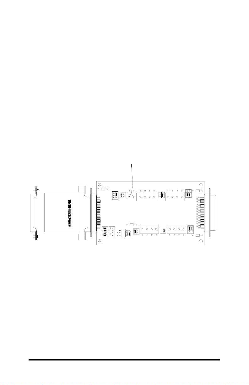
male side of the board. See Figure 1 for a system where the power is
brought directly onto the board. When passing power thro ugh from
another board, POWER is carried through on pin 2 and GND is carried
through on pin 7 . Powers flows in on the male DB25 co nnector and out on
the female DB25 connector with a 0.5 VDC drop across the board. This
allows multiple boards to be powered with a single power supply by
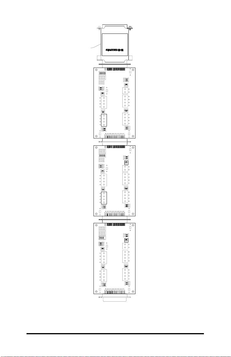
cascading them. See Table 4 for a list of B&B data acquisition products
that carry power t hrough on pins 2 a nd 7. Using these devices, you can
power an entire system with a single power supply as shown in Figure 2.
Power Supply
Port Powered
MODEL 232SDA10
D ATA A C QU IS ITION
Otta w a , Illin o is 6 1 35 0
MOD ULE
RS-232
GND
OFF.
OUT.
GAIN
R8
1
22.28/
USER
JP8
JP4
I/O P OR T
JP9
JP10
JP11
IN-
POWER
2.5V
0V
TB5
TB4
R2
TB2
JP6
22.28/U SE R
1
0V
2.5V
JP2
OFF.
OUT.
OFF
OUT
GAIN
OFF.
OUT.
IN+
GND
OFF
OUT
IN-
2.5V
0V
JP7
TB3
D
B
0V
2.5V
JP5
OFF.
OUT.
IN-
GND
OUT
IN+
GAIN
JP3
1
OFF
IN+
GND
OUT
22.28/
R7
USER
C
A
TB1
USER
22.28/
1
R1
JP1
IN-
GAIN
GND
IN+
OFF
Figure 1: Port Powered SDA and Powered Board
SDAIBB1300 Manual 3
B&B Electronics Mfg Co Inc – 707 Dayton Rd - PO Box 1040 - Ottawa IL 61350 - Ph 815-433-5100 - Fax 815-433-5104
Page 6
Power
N
IO
2
3
-2
E
L
U
IT
IS
U
Q
C
0
5
3
1
6
s
i
o
n
i
ll
I
I/O PORT
S
R
D
O
M
A
A
,
a
w
a
t
t
MODEL 232SDA10
T
A
D
O
GAIN
GAIN
GAIN
JP9
JP10
JP11
JP2
OUT.
OFF.
OUT
OFF
GND
IN+
IN-
OUT.
OFF.
OUT
OFF
GND
IN+
IN-
GAIN
JP9
JP10
JP11
JP2
OUT.
OFF.
OUT
OFF
GND
IN+
IN-
OUT.
OFF.
OUT
OFF
GND
IN+
IN-
GAIN
JP9
JP10
JP11
JP2
OUT.
OFF.
OUT
OFF
GND
IN+
IN-
OUT.
OFF.
OUT
OFF
GND
IN+
IN-
GAIN
R8
USER
1
22.28/
JP4
GAIN
JP8
0V
OUT.
22.28/USER
1
R2
0V
2.5V
JP6
TB2
B
JP5
0V
2.5V
A
TB1
JP1
22.28/
1
USER
R1
22.28/USER
1
R2
0V
2.5V
JP6
TB2
B
JP5
0V
2.5V
A
TB1
JP1
22.28/
1
USER
R1
22.28/USER
1
R2
0V
2.5V
JP6
TB2
B
JP5
0V
2.5V
A
TB1
JP1
22.28/
1
USER
R1
2.5V
TB5
TB4
D
0V
JP7
2.5V
TB3
C
22.28/
USER
R7
R8
USER
1
22.28/
JP4
JP8
0V
2.5V
TB5
TB4
D
0V
JP7
2.5V
TB3
C
22.28/
USER
R7
R8
USER
1
22.28/
JP4
JP8
0V
2.5V
TB5
TB4
D
0V
JP7
2.5V
TB3
C
22.28/
USER
R7
Board 1
OFF.
POWER
GND
ININ+
GND
OFF
OUT
OUT.
OFF.
ININ+
GND
OFF
OUT
JP3
GAIN
1
GAIN
OUT.
Board 2
OFF.
POWER
GND
ININ+
GND
OFF
OUT
OUT.
OFF.
ININ+
GND
OFF
OUT
JP3
GAIN
1
GAIN
OUT.
OFF.
Board 3
POWER
GND
ININ+
GND
OFF
OUT
OUT.
OFF.
ININ+
GND
OFF
OUT
JP3
GAIN
1
Figure 2: Single Power Supply System with 11 Channels Supported
4 SDAIBB1300 Manual
B&B Electronics Mfg Co Inc – 707 Dayton Rd - PO Box 1040 - Ottawa IL 61350 - Ph 815-433-5100 - Fax 815-433-5104
Page 7
Input Voltage Connections
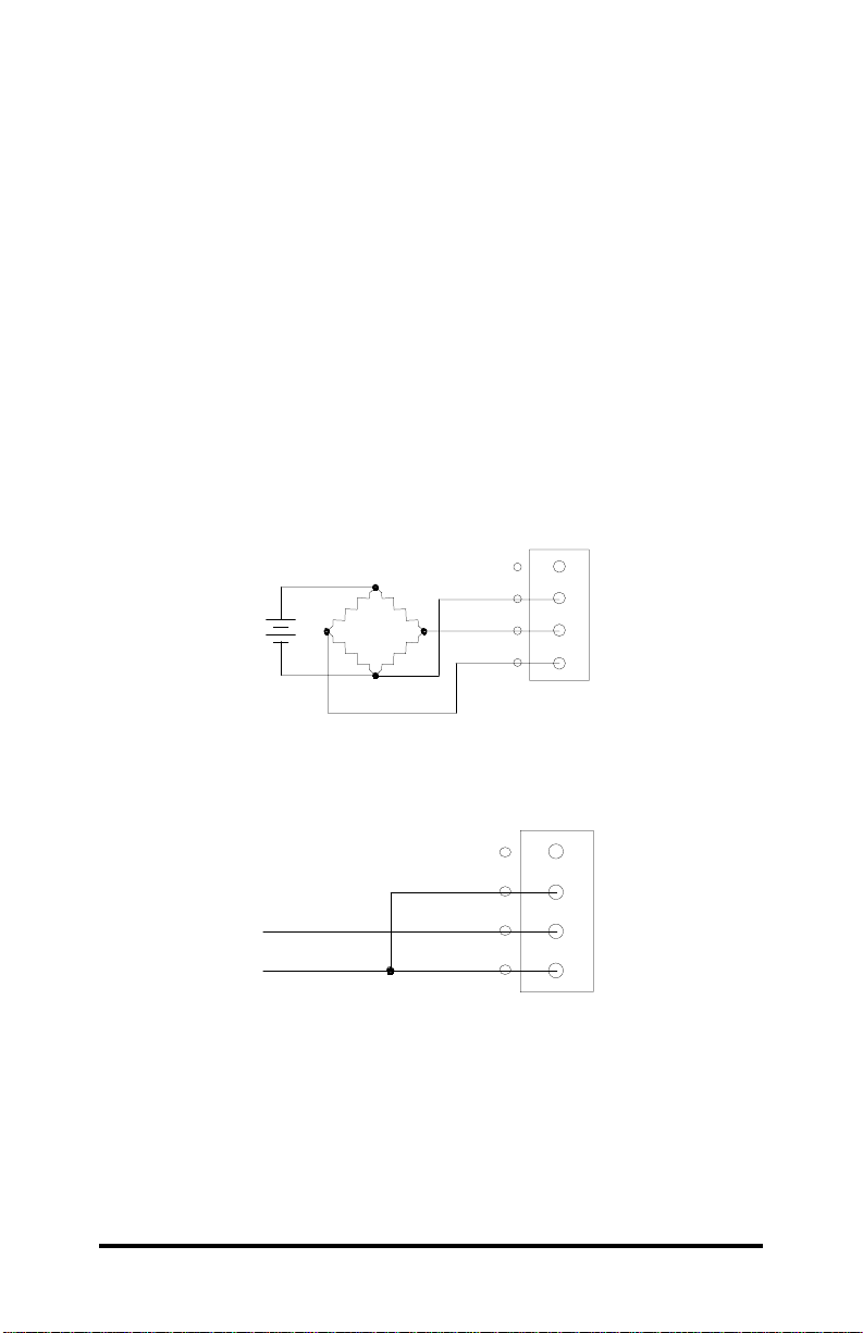
The SDAIBB can receive signals in the range of –0.15 to +5 VDC
when set to unity gain, and –0.15 to +3.5 VDC when set to any other gain.
Note: This voltage reading is taken from GND on the SDAIBB to
Input+ and GND to Input- voltage s. It is
from Input- to Input+.
blocks or solder pads. The terminal blocks are labeled Input+, Input-,
GND, and Output Offset. See Figures 3, 4, and 5 for typical input
configurations. The voltage that will be amplified is the reading taken from
Input- to Input+. GND is connected to the ground of the SDAIBB and is
provided for making a common reference for the SDAIBB and the input
device. The Output Offset is an input that shifts the output of the SDAIBB.
This feature is discussed further in Chapter 3, Output Offset.
Signals are brought into the buffer by terminal
Figure 3: Differential Signal with GND
not
the differential voltage
OUT
OFF
GND
IN+
IN-
OUT
OFF
GND
Signal
IN+
GND
Figure 4: Single Ended Signal
SDAIBB1300 Manual 5
B&B Electronics Mfg Co Inc – 707 Dayton Rd - PO Box 1040 - Ottawa IL 61350 - Ph 815-433-5100 - Fax 815-433-5104
IN-
Page 8

OUT
OFF
GND
IN+
IN-
Figure 5: Floating Differential Signal
Output Voltage Connections
The SDAIBB outputs voltages from +0.1 to +5.0 VDC at unity
gain, and +0.1 to +4.95 VDC at any other gain. All lines are carried
straight through on the DB25 connectors, allowing for the addition of extra
channels by connecting on another board.
The SDAIBB output connections are jumper selectable to line up
with the channels of the B&B line of SDAxx data acquisition devices.
When the 4-position shunt is set to JP9, input buffer A is connected to
channel 0 on pin 8, B is connected to channel 1 on pin 9, C is connected to
channel 2 on pin 10, and buffer D is connected to channel 3 on pin 11.
Setting the 4-position shunt to J P10 connects the buffers to channels 4 to 7
(pins 12, 13, 21, and 2 2 respectively), and setting the shunt to JP11
connects the buffers to channels 8 to 10 (pins 23 to 25). See Table 1 for a
list of the connections when the jumper is on JP9,
Table 2 for when the jumper is on JP10, and Table 3 for when the
jumper is on JP11.
buffer D is not connected to any pins on the DB25 connector.
For a listing of which modules the SDAIBB can connect to and
which channels are compatible on each module, see Table 4.
Note: When the 4-position jumper is on JP11,
6 SDAIBB1300 Manual
B&B Electronics Mfg Co Inc – 707 Dayton Rd - PO Box 1040 - Ottawa IL 61350 - Ph 815-433-5100 - Fax 815-433-5104
Page 9
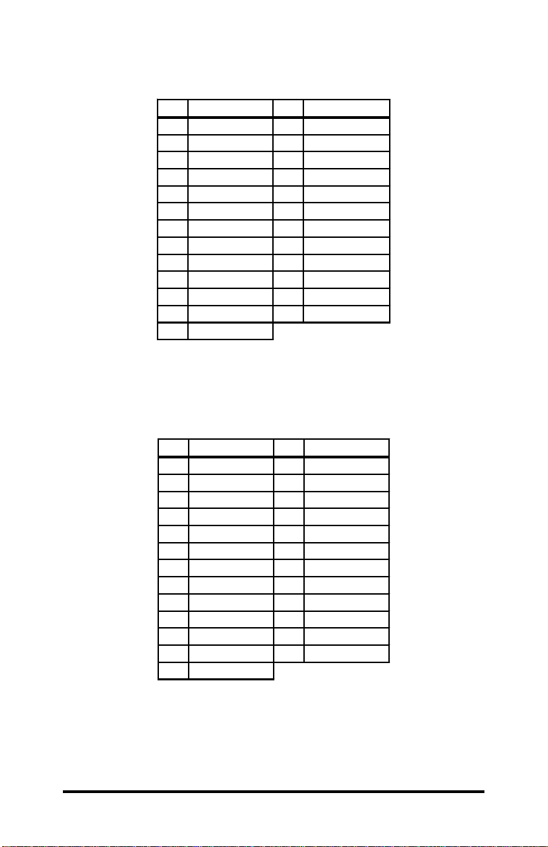
Table 1: Connections when the 4-posit ion shunt is on JP9
Pin Connection Pin Connection
1---14--2 Power 15 --3---16--4---17--5---18--6---19--7GND20 --8 A output 21 ---
9 B output 22 --10 C output 23 --11 D output 24 --12 --- 25 --13 ---
Table 2: Connections when the 4-posit ion shunt is on JP10
Pin Connection Pin Connection
1 --- 14 ---
2 Power 15 ---
3 --- 16 ---
4 --- 17 ---
5 --- 18 ---
6 --- 19 ---
7GND20 ---
8 --- 21 C output
9 --- 22 D output
10 --- 23 --11 --- 24 --12 A output 25 --13 B output
SDAIBB1300 Manual 7
B&B Electronics Mfg Co Inc – 707 Dayton Rd - PO Box 1040 - Ottawa IL 61350 - Ph 815-433-5100 - Fax 815-433-5104
Page 10

Table 3: Connections when the 4-posit ion shunt is on JP11
,
,
,
,
Pin Connection Pin Connection
1 --- 14 ---
2 Power 15 ---
3 --- 16 ---
4 --- 17 ---
5 --- 18 ---
6 --- 19 ---
7GND20 ---
8 --- 21 ---
9 --- 22 ---
10 --- 23 A output
11 --- 24 B output
12 --- 25 C output
13 ---
Table 4: Models Compatible with SDAIBB
Channel Select
Model
Jumper Connections
485SDA10 JP9
485SDA12 JP9
232SDA10 JP9
232SDA12 JP9
Channels
Supported
Supported
JP10, JP11 0-10 Yes Yes
JP10, JP11 0-10 Yes Yes
JP10, JP11 0-10 Yes Yes
JP10, JP11 0-10 Yes Yes
Power on
pins 2
and 7
Output
Offset
Available
232SPDA JP9 0-3 Yes Yes
232SPDACL JP9 0-3 Yes Yes
485SPDA JP9 0-3 Yes Yes
485SPDACL JP9 0-3 Yes Yes
232OPSDA * 4 and 5 No No
ADIO12 JP9 4-7 No No
2.5V
ADIO10 JP9 4-7 No No
Set the jumper for any position and use the solder pads on the DB25
connector to bring out connections for channels 4 and 5. The other
channels already have selectable gains.
To support all 11 channels on the SDAxx modules connect 3
SDAIBBs to the I/O port of the SDAxx as shown in Figure 2 on page 4 and
set one board to JP9, one to JP10, and the last to JP11. This will provide
11 independent buffered inputs.
8 SDAIBB1300 Manual
B&B Electronics Mfg Co Inc – 707 Dayton Rd - PO Box 1040 - Ottawa IL 61350 - Ph 815-433-5100 - Fax 815-433-5104
Page 11

Chapter 3: Configuration
Output Offset
The output offset is the amount by which the output is shifted.
Equation 1 shows how the output offset affects the output of the buffer.
The negative output rail will clip any reading that has a negative input
differential unless the buffer’s output offset is raised. For this purpose,
output offsets of 0 V and 2.5 V are individually jumper selectable for each
channel on the SDAIBB when mated with a compatible data acquisition
model. JP5 corresponds to channel A, JP6 corresponds with channel B,
JP7 corresponds with channel C, and JP8 corresponds with channel D.
An output offset of 0 V is always available. See Table 4 for a list
of models that support the 2.5 V output offset. An output offset of 0 V is
used for positive only differentials, and an output offset of 2.5 V provides
the maximum input range for signals that run equally positive and negative.
A different output offset may be brought in on the ter minal blocks
with the output offset jumper removed on the corresponding channel.
Equation 1:
()
out
−+
+−=
etOutputOffsGainININV
Gain Selection
The gain is individually selectable on each buffer with a twoposition jumper. Gains of 1 and 22.28 are conveniently provided on the
unit for each buffer. JP1 controls the gain on channel A, JP2 controls B,
JP3 controls C, and JP4 controls D. Unity gain is ideal for eliminating the
impedance mismatch between input devices and the data acquisition
module. Table 5 shows the maximum voltage ranges that can be amplified
by the provided gain of 22.28. To change the gain, leave the jumper in the
User/22.28 gain position, remove the through-hole 4.7 kΩ resistor, and
replace it with the appropriate value. See Table 6 for some standard inputs,
gains, and appropriate resistor values to achieve the expected gain.
SDAIBB1300 Manual 9
B&B Electronics Mfg Co Inc – 707 Dayton Rd - PO Box 1040 - Ottawa IL 61350 - Ph 815-433-5100 - Fax 815-433-5104
Page 12

Table 5: Values for Use with the Provided Gain of 22.28
VCM VDIFF Out Ref
27.5 mV max +55 mV 0 V 4.7 k
0 V ±52 mV 2.5 V 4.7 k
2.5 V ±110 mV 2.5 V 4.7 k
1%
Resistor
Calculated
Gain
22.28 0.01 – 1.23 V
Ω
22.28 1.32 - 3.68 V
Ω
22.28 0.03 - 4.97 V
Ω
Output
Range
Table 6: Gains and Resistor Values for St andard Inputs
CM
V
V
DIFF
Out
Ref
5mV max +10 mV 0V 119
50mV max +100mV 0V 12.8
0.5V max +1 V 0V 2.18
0V ±10 mV 2.5V 118
0V ±100 mV 2.5V 11.8
2.5V ±10 mV 2.5V 247
2.5V ±100 mV 2.5V 24.7
2.5V ±1 V 2.5V 2.47
MAX
G
Closest 1%
Resistor
866
8.66 k
86.6 k
866
9.31 k
412
4.32 k
69.8 k
Calculated
Gain
116.47 0.01 - 1.16 V
12.55 0.01 - 1.25 V
2.15 0.01 - 2.18 V
116.47 1.34 - 3.66 V
11.74 1.32 - 3.67 V
243.72 0.06 - 4.94 V
24.15 0.09 - 4.91 V
2.43 0.07 - 4.93 V
Output
Range
Change R1 to change t he gain on channel A, R2 to change channel
B, R7 to change channel C, and R8 to change channel D. The following
sections explain how to calculate the gain and gain resistor for other input
ranges.
10 SDAIBB1300 Manual
B&B Electronics Mfg Co Inc – 707 Dayton Rd - PO Box 1040 - Ottawa IL 61350 - Ph 815-433-5100 - Fax 815-433-5104
Page 13

4c4
Maximum Gain
The maximum gain for a known differential vol tage and common
mode voltage can easily be determined using the following set of equations.
Equation 5 calculates the maximum gain based on the positive internal rail
of the amplifier. Equation 6 gives the maximum gain based on the negative
internal rail of the amplifier. Equation 7 calculates the maximum gain
without overflowing the output range of the SDAIBB. The smallest
maximum gain value calculated using these equations is the maximum gain
that may be used.
−
Equation 2:
Equation 3:
Equation 4:
()
=
G
MAX
()
=
G
max
G
MAX
94.4
=
VV
4.42
V
DIFF
+
59.02
cm
V
DIFF
V
InputRange
CM
VV
G is the gain, V
is the common mode voltage, and V
cm
diff
differential voltage.
Example:
Find the maximum allowable gain for a differential voltage of
±10 mV and a common mode voltage of 2.5 V.
−
()
From Equation 5:
From Equation 6:
From Equation 7: 247
=
G
MAX
()
=
G
max
G
MAX
94.4
5.24.42
=
01.0
+
01.0
02.0
380
59.05.22
=
618
==
The minimum value calculated is 247, so the maximum allowable gain is
247.
SDAIBB1300 Manual 11
B&B Electronics Mfg Co Inc – 707 Dayton Rd - PO Box 1040 - Ottawa IL 61350 - Ph 815-433-5100 - Fax 815-433-5104
is the
Page 14

Gain Resistor Determination
Replacing a single resistor changes the gain on each buffer.
Change R1 to modify the gai n on channel A, R2 to change channel B, R7
to change channel C, and R8 to change channel D. Use Equation 8 to
determine the value of the gain resistor to attain a calculated gain. To use
this gain value, place the gain jumper corresponding to the correct channel
in the User/22.28 position. JP1 corresponds to channel A, JP2 corresponds
to channel B, JP3 corresponds to channel C, and JP4 corresponds to
channel D.
Ω
100
k
=
Equation 8:
Equation 9:
R
is the value of the gain resistor in ohms.
G
R
G
kGΩ
100
1
+=
()
−
1
G
R
G
Example:
Find the appropriate 1% resistor for a maximum gain of 150 and
calculate the actual gain.
From Equation 8:
R
G
100000
=
1150
()
−
141.671
=
The nearest 1% resistor that will produce a gain of 150 or less is 681Ω.
From Equation 9: 8.147
100000
1 =+=G
681
The nearest 1% resistor is 681Ω with a resulting gain of 147.8.
12 SDAIBB1300 Manual
B&B Electronics Mfg Co Inc – 707 Dayton Rd - PO Box 1040 - Ottawa IL 61350 - Ph 815-433-5100 - Fax 815-433-5104
Page 15

Maximum and Minimum Common Mode Voltage
If the differential voltage range and desired gain are known, the
maximum and minimum common mode voltage can b e determined.
Equation 10 is used to calculate the maximum common mode voltage
knowing the gain and the differential voltage. Equation 11 is used to
calculate the minimum common mode voltage. Remember that when
Input+ or Input- is connected to GND on the SDAIBB the
common mode voltage c hanges as the differ ential voltage changes.
×
DIFF
−=
Equation 10:
Equation 11:
CMMAX
CMMIN
4.4GVVV
+−=
590.0GVVV
2
DIFF
×
2
Example:
Find the allowable range of the co mmon mode voltage for a
input range of ±100 mV with a gain of 10.
From Equation 10:
From Equation 11:
CMMAX
CMMIN
4.4
590.0
101.0
−=
2
+−=
VV
9.3
=
101.0
×
−=
2
×
The common mode voltage must be between –0.09 and 3.9 V.
VV
09.0
SDAIBB1300 Manual 13
B&B Electronics Mfg Co Inc – 707 Dayton Rd - PO Box 1040 - Ottawa IL 61350 - Ph 815-433-5100 - Fax 815-433-5104
Page 16

Maximum Differential
To determine the maximum differential voltage that can be
amplified, the gain and the common mode voltage must be known first.
Using this information, the most positive the differential voltage may be is
calculated using Equation 12. Equation 13 is used to calculate the most
negative that the differential voltage may swing. These two values are still
limited by the maximum allowable swing given by Equation 14.
−
V
4.42
()
Equation 12:
Equation 13:
Equation 14:
=
V
DIFF
=
V
DIFF
InputRange
CM
G
()
CM
≤
+
590.02
VV
G
V
94.4
G
Example:
Find the allowable swing of a signal with a common mode
voltage of 1V with a gain of 50.
From Equation 12:
From Equation 13:
From Equation 14: 0988.0
=
V
DIFF
V
DIFF
50
()
=
50
590.012 +
94.4
136.0
0636.0
=≤InputRange
50
14.42=−
()
The differential voltage can swing as negative as –0.0636 V and as positive
as 0.136 V. However, this full range cannot be achieved with the same
output offset setting due to the 0.0988 V range from Equation 14. To find
the output offset voltage that allows the lower end of this range, use
Equation 1 with Vout set to 0.01 V.
()
out
+−=
−+
etOutputOffsGININV
Rearranged to calculate the desired output offset it looks like this
×−=
GVVetOutputOffs
DIFFout
Substitute in the appropriate values and solve for the output offset.
()
VetOutputOffs 19.3500636.001.0 =×−−=
14 SDAIBB1300 Manual
B&B Electronics Mfg Co Inc – 707 Dayton Rd - PO Box 1040 - Ottawa IL 61350 - Ph 815-433-5100 - Fax 815-433-5104
Page 17

Example Board Setup
Figure 6 is an example of one possible configuration for the
SDAIBB without modifying the board. Table 7 lists the setup for each
channel.
Table 7: Setup for Figure 6
Channel Output Pin Gain Output Offset
A 8 22.28 2.5 V
B 9 1 0.0 V
C 10 1 2.5 V
D 11 22.28 0.0 V
SDAIBB1300 Manual 15
B&B Electronics Mfg Co Inc – 707 Dayton Rd - PO Box 1040 - Ottawa IL 61350 - Ph 815-433-5100 - Fax 815-433-5104
Page 18

JP9
JP10
JP11
JP2
GAIN
OUT.
2.5V
OFF.
OUT
OFF
GND
IN+
IN-
JP5
OUT.
OFF.
OUT
OFF
GND
IN+
IN-
JP1
GAIN
22.28/USER
1
0V
0V
2.5V
1
R1
JP6
22.28/
USER
TB2
A
TB1
R2
TB5
TB4
DB
TB3
C
JP4
JP8
JP7
USER
22.28/
22.28/
USER
1
R7
R8
GAIN
0V
2.5V
POWER
ININ+
GND
OFF
OUT
0V
2.5V
ININ+
GND
OFF
OUT
1
OUT.
OFF.
GND
OUT.
OFF.
JP3
GAIN
Figure 6
16 SDAIBB1300 Manual
B&B Electronics Mfg Co Inc – 707 Dayton Rd - PO Box 1040 - Ottawa IL 61350 - Ph 815-433-5100 - Fax 815-433-5104
Page 19

Appendix A: Glossary
()
Common Mode Voltage
voltage swings. When this is measured on the SDAIBB it is calculated
with all voltage readings taken in reference to GND of the SDAIBB as
+ ININ
()
−+
. Note that when one of the inputs is connected to GND of
2
the SDAIBB the common mode voltage changes as the differential voltage
changes.
Differential Voltage
such as the two leads on a thermocouple. When this is measured on the
SDAIBB it is calculated with all voltage readings taken in reference to
GND of the SDAIBB as
G: The amount by which the input is multiplied before it is output.
()
Gain
V
out
=
Gain
−
ININ
−+
Impedance Mismatch:
enough from the input impedance of the d a ta acquisition device to cause
improper sensor readings.
Negative Input Differential:
voltage at IN-. 0≤−
Negative Rail:
The lowest possible voltage that can be output. For the
SDAIBB there is a negative rail internal to the buffer and a negative rail on
the output of the buffer.
Positive Rail:
The highest possible voltage that can be output. For the
SDAIBB there is a positive rail internal to the buffer and a positive rail on
the output of the buffer.
V: The voltage about which a differential
CM
V
()
The difference in voltage across two points
:
DIFF
ININ
.
−
−+
When the output impedance of sensor is different
When the voltage and IN- is higher than the
ININ
−+
SDAIBB3599 Manual A-1
B&B Electronics Mfg Co Inc – 707 Dayton Rd - PO Box 1040 - Ottawa IL 61350 - Ph 815-433-5100 - Fax 815-433-5104
Page 20

Appendix B: Error Budget Calculations
Important Specs @ 25°C:
offset in
V
V
I offset
Gain Error 0.35%
Gain Nonlinearity 50ppm
0.1Hz to 10Hz Noise 3.0µV p-p
CMR 84dB @ 60 Hz
Error Contributions that can be Removed With
Calibration
V 200 µV
()
OSI
offset out
I 2nA
()
OS
V
()
OSO
Equation 15:
Equation 16:
=
V
OS
I
=
OS
1000 µV
V
+
V
OSI
V
in
OSO
V
G
I
ImpedanceSensor
×
os
in
Equation 17:
Equation 18:
V
is the input voltage.
in
Error CMR
ppm3500ErrorGain =
×
Vppm
4
=
CM
V
in
Error Contributions that Cannot be Removed with
Calibration
Equation 19:
Equation 20:
=
noise 10Hz - 0.1Hz
SDAIBB3599 Manual B-1
B&B Electronics Mfg Co Inc – 707 Dayton Rd - PO Box 1040 - Ottawa IL 61350 - Ph 815-433-5100 - Fax 815-433-5104
ppm50tyNonlineariGain
nV3000
=
V
in
Page 21

Example:
Calculate the error budget for a 350Ω, 100mV load cell with a
common mode voltage of 2.5V using a gain of 22.28.
From Equation 15: ppm
From Equation 16:
200
=
V
OS
I
=
OS
100
×Ω
mV
2503
100
nA
mV
=
7
ppm
µ
V
500
µ
+
V
From Equation 17: ppm3500ErrorGain =
From Equation 18:
=
Error CMR
From Equation 19:
From Equation 20: ppm
×
mV
100
=
noise 10Hz - 0.1Hz ==
3000
Total Unadjusted Error = 6109ppm
Error After Calibration = 53ppm
28.22
2449
=
Vppm
5.24
=
100
ppm50tyNonlineariGain
nV
100
ppm
mV
3
B-2 SDAIBB3599Manual
B&B Electronics Mfg Co Inc – 707 Dayton Rd - PO Box 1040 - Ottawa IL 61350 - Ph 815-433-5100 - Fax 815-433-5104
Page 22

FEDERAL COMMUNICATIONS COMMISSION
RADIO FREQUENCY INTERFACE STATEMENT
Class A Equipment
This equipment has been tested and found to comply with the
limits for Class A digital device, pursuant to Part 15 of the FCC
Rules. These limits are designed to provide reasonable protection
against harmful interference when the equipment is operated in a
commercial environment. This equipment generates, uses, and can
radiate radio frequency energy and, if not installed and used in
accordance with the instructions, may cause harmful interference to
radio communications. Operation of this equipment in a residential
area is likely to cause harmful interference, in which case the user
will be required to correct the interference at personal expense.
FCC Class A Equipment Statement
 Loading...