Bay Linear LM2941S, LM2941N, LM2941J, LM2940T, LM2941T Datasheet
...
Bay Linear, Inc
2478 Armstrong Street, Livermore, CA 94550 Tel: (925) 989-7144, Fax: (925) 940-9556 www.baylinear.com
1.25A High Current Low Dropout
LM2940/2941
Voltage Regulator Adjustable
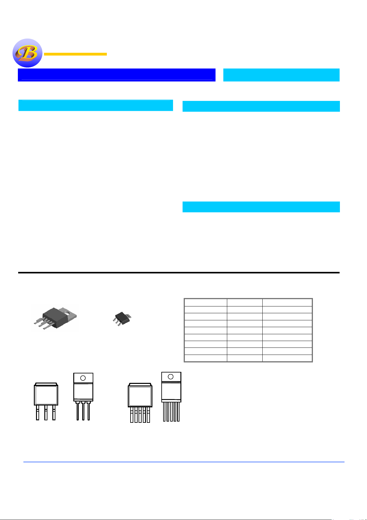
Pin Connection
Ordering Information
Devices Package Temp.
LM2940T TO-220-3
-40 °C to 125 °C
LM2941T TO-220-5
-40 °C to 125 °C
LM2940S TO-263-3
-40 °C to 125 °C
LM2941S TO-263-5
-40 °C to 125 °C
LM2940N SOT-223-3
-40 °C to 125 °C
LM2941N SOT-223-5
-40 °C to 125 °C
LM2940J LPDD-3
-40 °C to 125 °C
LM2941J LPDD-5
-40 °C to 125 °C
Description
The Bay Linear LM2940 & LM2941 is a 1.25A high accuracy, low
dropout voltage regulator with only 40mV at light loads and
350mV(Typ.)@ 1.0A) and low quiescent current of 240µA typical.
The LM2940/41 is designed for low voltage a application that
requires lower dropout voltage and faster transient response. This
device is an excellent choice for use in powering low voltage
applications where require a lower dropout, faster transient response
to regulate from +2.5V to 3.8V supplies and as a post regulator for
switching supplies applications.
The LM2940/41 offers full protection against over-current faults,
reversed input polarity, reversed load insertion, and positive and
negative transient voltage. On-Chip trimming adjusts the reference
voltage to 1%. The LM2940-xx devices are in 3 pin fixed voltage
regulators. The LM2941 include an Enable pin in the 5 pin
packages
.
The LM2940/41 are offered in a 3 & 5-pin SOT-223, TO-220 &
TO-263 package compatible with other 3 terminal regulators. The
LM2940/41 is also offer in a new LPDD (Low Profile TO-263)
package from 4.47 mm (DD) tickness down to only 1.27 mm
Features
• High output accuracy of 1%
• Output Adjustable from 1.24V to 26V
• Output Current of 1.25A
• Low Dropout Voltage
• Low quiescent current
• Extremely Tight Load & Line Regulation
• Reverse-battery and “Load Dump” Protection
• Zero Current Shutdown Mode (5-pin version)
• Offer in TO-263, TO-220, SOT-223, & New Slim
LPDD
• Similar to industry Standard MIC2940LM2941
Applications
• Powering VGA & Sound Card
• LCD Monitor
• Battery Powered Equipments/Laptop & Notebook
• SMPS Post Regulator / DC to DC Modules
• High Efficiency Linear Power Supply
• Adjustable Power Supply
Bay Linear
Inspire the Linear Power
TO-263-3 Package
V
OUT
GND
V
IN
BAY
B2940
Front View
123
Front View
TO-220-3 Package
BAY
B2940
V
IN
V
OUT
GND
TO-263-5 Package
Top View
45
BAY
B2941
321
GND
OUPUT
1)
3)
4)
5)
2)
ON/OFF
ADJUST
INPUT
TO-220-5 Package
Top View
BAY
B2941
12345
TO-263-3 Package
V
OUT
GND
V
IN
BAY
B2940
Front View
123
Front View
TO-220-3 Package
BAY
B2940
V
IN
V
OUT
GND
TO-263-3 Package
V
OUT
GND
V
IN
BAY
B2940
Front View
123
Front View
TO-220-3 Package
BAY
B2940
V
IN
V
OUT
GND
Front View
TO-220-3 Package
BAY
B2940
V
IN
V
OUT
GND
TO-263-5 Package
Top View
45
BAY
B2941
321
GND
OUPUT
1)
3)
4)
5)
2)
ON/OFF
ADJUST
INPUT
TO-220-5 Package
Top View
BAY
B2941
12345
TO-263-5 Package
Top View
45
BAY
B2941
321
GND
OUPUT
1)
3)
4)
5)
2)
ON/OFF
ADJUST
INPUT
GND
OUPUT
1)
3)
4)
5)
2)
ON/OFF
ADJUST
INPUT
TO-220-5 Package
Top View
BAY
B2941
12345
TO-220-5 Package
Top View
BAY
B2941
12345

Bay Linear, Inc
2478 Armstrong Street, Livermore, CA 94550 Tel: (925) 989-7144, Fax: (925) 940-9556 www.baylinear.com
LM2940/41
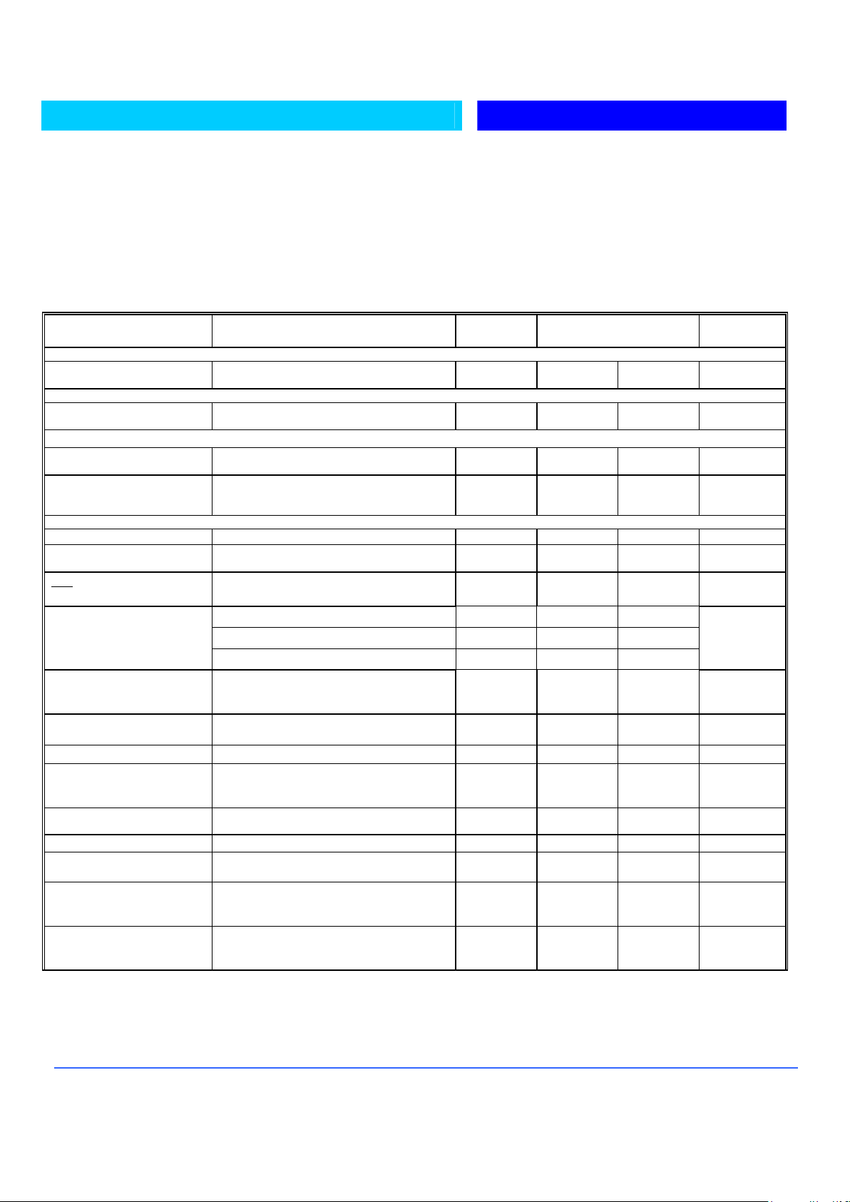
ABSOLUTE MAXIMUM RATINGS
Lead Temp. (Soldering, 5 Seconds).................................260°C Input Voltage ........................................................26V
Storage Temperature Range.............................. -65° to +150°C Maximum Output Current....................................3.5A
Operating Junction Temperature Range Input Supply Voltage (Note1) (Survival)-20V to +60V
LM2940/2941 Control Section.................. -45°C +125°C
LM2940/2941 Power Transistor.................-45°C +150°C
ELECTRICAL CHARACTERISTICS (NOTE 1) at I
OUT
= 5mA, V
IN
=V
OUT
+ 1V, I l = 1000mA, C L = 10µF. Ta=25°C, unless otherwise
specified. The LM2941 is programmed to output 5V and has V
SHUTDOWN
≤ 0.6V
PARAMETER CONDITIONS Typ LM2940
Min Max
Units
2.5V Version
Output Voltage (Note 2)
I
OUT
= 5mA
5mA ≤I
OUT
≤1.25A, 4.75V≤V
IN
≤26V
2.5
2.5
2.475
2.450
2.525
2.550
V
3.3V Version2.
Output Voltage (Note 2)
I
OUT
= 5mA
5mA ≤I
OUT
≤1.25A, 4.75V≤V
IN
≤26V
3.3
3.3
3.267
3.234
3.330
3.366
V
5.0V Version
Output Voltage (Note 2)
I
OUT
= 5mA
5mA ≤I
OUT
≤1.25A, 5.5V≤V
IN
≤26V
5.0
5.0
4.95
4.90
5.05
5.10
V
Output Voltage
Accuracy
5mA ≤I
OUT
≤1.0 A
-1
-2
-2.5
1
2
2.5
%
All Voltage Options
Line Regulation
IO = 5mA, (V
OUT
+ 1V) ≤ VIN≤ 26V
0.06
0.5 %
Load Regulation
VIN = V
OUT
+ 5V, 5mA ≤ I
OUT
≤ 1 A
(Note 2, 6)
0.2 1.6 %
∆V°
20
100
ppm/°C
∆T
Output Voltage (Note 6)
Temperature Coef.
IO = 5mA
80 150
IO = 1000mA
350 450
Dropout Voltage
I
O
= 1.25A
400 600
mV
Ground Current IO = 5mA, VIN = V
OUT
, +1V
I
O
= 1000mA, VIN = V
OUT
, +1V
I
O
= 1.25A
240
22
35
350
35
70
µA
mA
I
GNDDO
Ground Pin Current at
Dropout
VIN = 0.5V less than specified V
OUT IOUT
= 10mA 0.9
mA
Current Limit
V
OUT
= 0V (Note 4) 1.7 1.5
A
Output Noise Voltage
(10Hz to 100kHz)
IL = 100mA
CL = 10µF
C
L
= 33µF
400
260
µV
RMS
Reference Voltage
1.235 1.223
1.210
1.247
1.260
V
V
max
Reference Voltage
(Note 8)`
1.204 1.266
V
Adjust Pin
Bias Current
40 80
120
nA
Reference Voltage
Temperature
Coefficient
(Note 7) 20
ppm/°C
Adjust Pin Bias
Current Temperature
Coefficient
0.1
nA/°C
 Loading...