Bay Linear LM2576T-15, LM2576T-5, LM2576T-3.3, LM2576T-ADJ, LM2576J-12 Datasheet
...
Bay Linear, Inc
2418 Armstrong Street, Livermore, CA 94550 Tel: (925) 606-5950, Fax: (925) 940-9556 www.baylinear.com
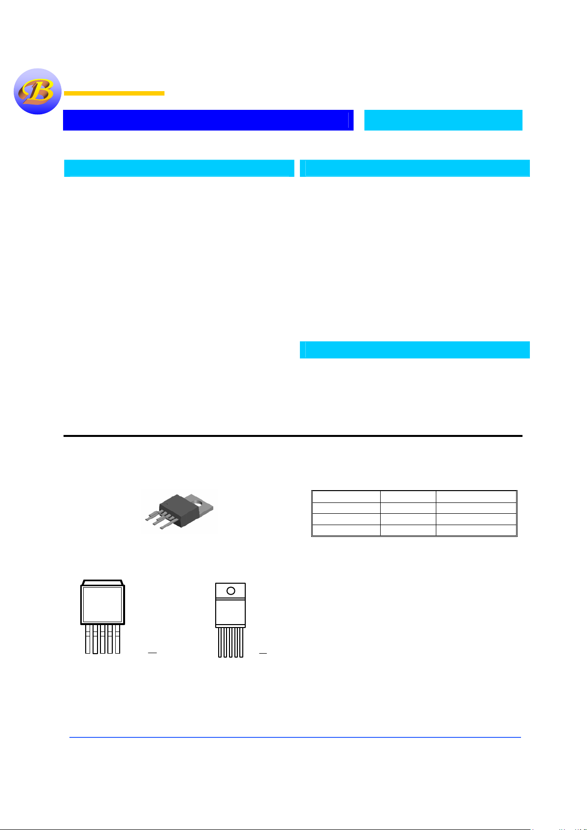
PIN CONNECTIONS
3.0A Step Down Switching voltage Regulator
LM2576
Adjustable & Fix Output
Pin Connection
Ordering Information
Devices Package Temp.
LM2576T-X TO-220
-40 °C to 125 °C
LM2576S-X TO-263
-40°C to 125 °C
LM2576J-X LPDD
-40°C to 125 °C
X= Output Voltage (X=3.3V, 5.0V, 12V, 15V or Blank for Adjustable)
Consult factory for other fixed voltages.
Description
The Bay Linear LM2576 contains fixed and adjustable
switching voltage regulators that require a minimum of
external components. All circuitry necessary to build a
buck-switching regulator is included.
The LM2576 is available in 3.3V; 5V, 12V & 15V fixed
voltages, or an adjustable version with an output voltage
range from 1.23V to 37V. The guaranteed accuracy for
specified input and load conditions is ±4%.
The LM2576 can supply 3A with an excellent load and
line regulation. Protection such as cycle-by-cycle
current limiting or thermal shutdown has been designed.
In standby mode, the current consumption has been
minimized (200µA).
For 1A step-down switching regulators refer to B2575
data sheets
Features
• Guaranteed 3A Output Current
• High Efficiency
• Wide Input Voltage, up to 40V
• 3.3V, 5V, 12V, 15V and Adjustable Output
Versions
• Thermal Shutdown and Current Limit
Protection
• Requires only 4 External Components
• Low Power Standby Mode < 200µA Typical
• Shutdown Capability (Standby Mode)
• 52kHz Fixed Frequency Internal Oscillator
• Uses Standard Inductors
• Pin-to-Pin Compatible with LM2576
Applications
• Efficient Pre-Regulator for Linear Regulators
• On-card Switching Regulators
• Positive to Negative Converter (Buck-Boost)
• Simple High-efficiency Step-down (Buck)
•
Portable Instruments
TO-263-5 Package
Top View
45
BAY
B2576
GND
V
OUT
V
IN
1)
3)
4)
5)FBON/OFF
2)
1
2
3
TO-220-5 Package
Top View
GND
V
OUT
VIN1)
3)
4)
5)
2)
FB
ON/OFF
54321
BAY
B2576
Bay Linear
Inspire the Linear Power

Bay Linear, Inc
2418 Armstrong Street, Livermore, CA 94550 Tel: (925) 606-5950, Fax: (925) 940-9556 www.baylinear.com
LM2576
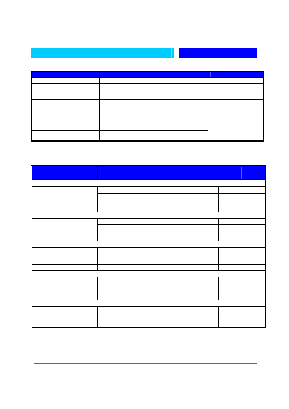
Absolute Maximum Rating
Parameter Symbol Value Unit
Maximum Input Voltage V
IN
45 V
Power Dissipation P
O
Internally Limited W
Off Pin Input Voltage
-0.3V<V<V
IN
Output Voltage
-1 V
Supply Voltage
40 V
Operating Junction
Temperature Range
Control Section
Power Transistor
T
J
-40<TJ<85
Storage Temperature Range T
STG
-65 to 150
Lead Temperature (Soldering 10
Sec.)
T
LEAD
260
°C
ELECTRICAL CHARACTERISTICS
T
A
= 25°C VIN = 12V, I
LOAD
= 100mA unless otherwise specified.
Boldface type applies over full Operating Temperature Range
.
Parameter Conditions LM2576
Typ Min Max
Units
Adjustable Regulators
(
Note 3)(Note 8
)
VIN = 12V, I
LOAD
= 0.5A, V
OUT
= 5V 1.230 1.217 1.243 V
Output Voltage (V
OUT
)
0.5A ≤ I
LOAD
≤ 3A, 6V≤ V
IN
≤ 40V, V
OUT
=
5V
1.230
1.230
1.193
1.180
1.267
1.280
V
Efficiency (Note 7) VIN = 12V, I
LOAD
= 3A, V
OUT
= 5V 82 %
3.3V Version (Note 3)(Note 9)
VIN = 12V, I
LOAD
= 0.5A, V
OUT
= 3.3V 3.3 3.234 3.366 V
Output Voltage (V
OUT
)
0.5A ≤ I
LOAD
≤
3A, 6V ≤ VIN ≤ 40V,
V
OUT
= 3.3V
3.3
3.3
3.168
3.135
3.432
3.465
V
Efficiency VIN = 12V, I
LOAD
= 3A 75 %
5V Version (Note 3)(Note 9)
VIN = 12V, I
LOAD
= 0.5A, V
OUT
= 5V 5.0 4.900 5.100 V
Output Voltage (V
OUT
)
0.5A ≤ I
LOAD
≤
3A, 8V ≤ VIN ≤ 40V,
V
OUT
= 5V
5.0
5.0
4.800
4.750
5.200
5.250
V
Efficiency (Note 7) VIN = 12V, I
LOAD
= 3A, V
OUT
= 5V 82 %
12V Version (Note 3)(Note 9)
VIN = 25V, I
LOAD
= 0.5A, V
OUT
= 12V 12 11.760 12.240 V
Output Voltage (V
OUT
)
0.5A ≤ I
LOAD
≤
3A, 15V ≤ VIN ≤ 40V,
V
OUT
= 12V
12
12
11.520
11.400
12.480
12.600
V
Efficiency (Note 7) VIN = 25V, I
LOAD
= 3A 88 %
15V Version(Note 3)(Note 9)
VIN = 30V, I
LOAD
= 0.5A, V
OUT
= 15V 15 14.700 15.300 V
Output Voltage (V
OUT
)
0.5A ≤ I
LOAD
≤ 3A, 18V ≤ VIN ≤ 40V,
V
OUT
= 15V
15
15
14.400
14.250
15.600
15.750
V
Efficiency (Note 7) VIN = 30V, I
LOAD
= 3A 88 %

Bay Linear, Inc
2418 Armstrong Street, Livermore, CA 94550 Tel: (925) 606-5950, Fax: (925) 940-9556 www.baylinear.com
LM2576
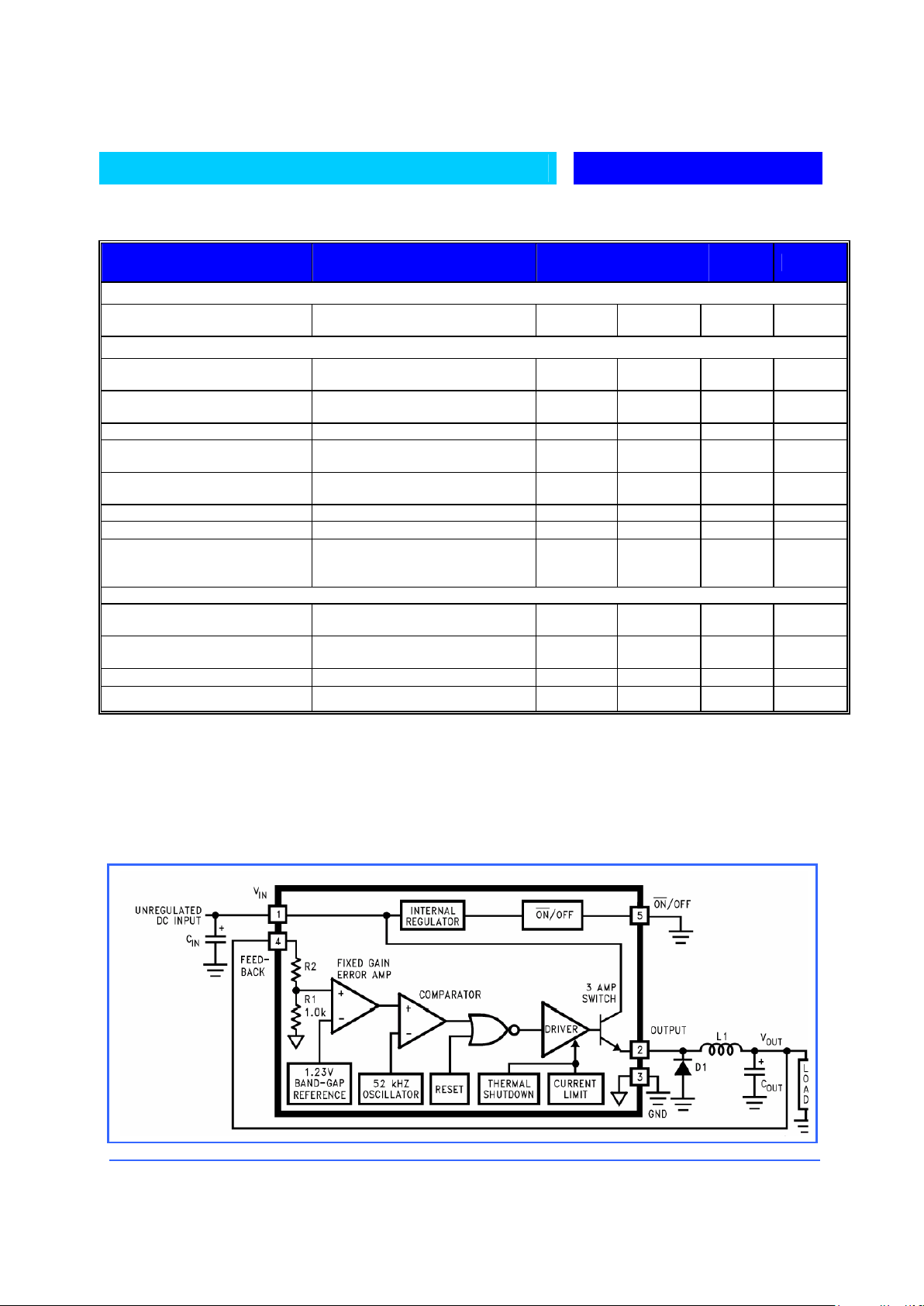
ELECTRICAL CHARACTERISTICS TA = 25°C VIN = 12V, I
LOAD
= 100mA unless otherwise specified.
Boldface type applies over full Operating Temperature Range.
Parameters Conditions
Typ
LM2576
Min
Max
Units
Adjustable Regulator
Feedback Bias Current V
OUT
= 5V 50
100
500
nA
Fixed and Adjustable Regulators
Oscillator Frequency 52
47
42
58
63
kHz
Saturation Voltage I
OUT
= 0.5A, (Note 4) 1.4
1.8
2.0
V
Max Duty Cycle (Note 5) 98 93 %
Current Limit
Peak Current, t
ON
≤ 3µs, (Note 4)
5.8
4.2
3.5
6.9
7.5
A
Output Leakage Current
V
IN
, (Note 6), Output = 0V
(Note 6 ), Output = -1V
7.5
2
30
mA
Quiescent Current (Note 6) 5 10 mA
Standby Quiescent Current ON/OFF Pin = 5V (OFF) 50 200
µA
Thermal Resistance
T,U package, Junction to Ambient,
(Note 7)
T,U package, Junction to case
65
2
°C/W
ON/OFF Control, Fixed & Adjustable Regulators (Note 8) (Note9)
OFF Input Level V
OUT
= 0V 1.4
2.2
2.4
V
ON Input Level V
OUT
= 15V or 5V 1.2
1.0
0.8
V
OFF Logic Current ON/OFF Pin = 5V (OFF) 4 30
µA
ON Logic Current ON/OFF Pin = 0V (ON) 0.01 10
µA
Note 1: Absolute Maxium Ratings indicate limits beyond which damage to the device may occur. Operating Ratings indicate test conditions for which the device s
intended to be functional, but do not guarantee specific performance limits. For quaranteed specifications and test conditions see the Electrical Characteristics.
Note 2: All limits guaranteed at room temperature (standard type face) and at temperature extremes (bold type face). All room temperature limits are 100%
production tested. All limits at temperature extremes are guaranteed via testing.
Note 3: External components such as the diode, inductor and capacitor can affect the system performance.
Note 4: Output (pin 2) sourcing current. No diode, inductor, or capacitor connected to input.
Note 5: Feedback (pin 4) removed from output and connected to 0V.
Note 6: Feedback (pin 4) removed from output and connected to 12V to force the output transistor OFF.
Note 7: Junction to ambient thermal resistance with approximately 1 square inches of PC board cooper surrounding the leads.
Note 8: Test circuit refers to figure 2.
Note 9: Test circuit refers to figure 3.
 Loading...