Bay Linear IRL820T, IRL820S Datasheet

Bay Linear, Inc
2478 Armstrong Street, Livermore, CA 94550 Tel: (925) 606-5950, Fax: (925) 940-9556 www.baylinear.com
POWER MOSFET
IRF820
Advance Information
Ordering Information
Device Package Temp.
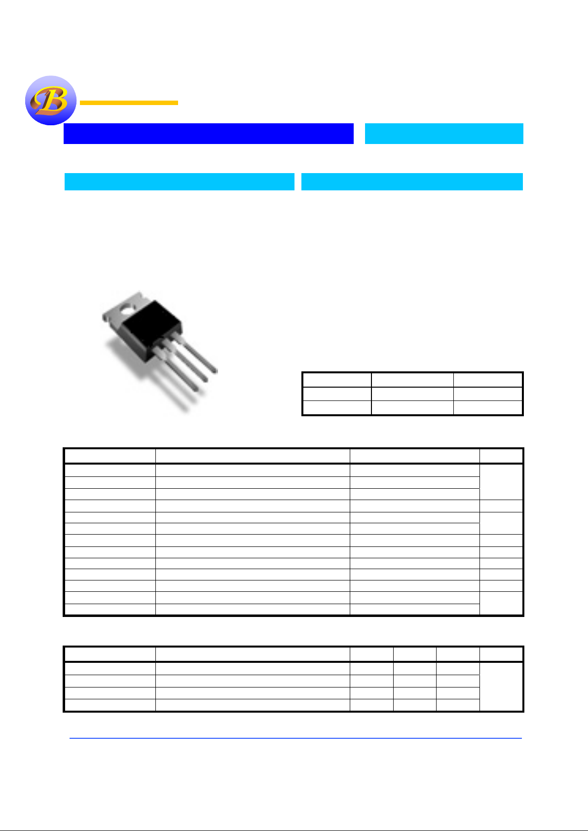
IRL820T TO-220
0 to 150°C
IRL820S TO-263 ( D2 )
0 to 150°C
Absolute Maximum Rating
Parameter Max Unit
ID@ TC =25°°°°C
Continuous Drain Current , V
GS
@10V 2.5
ID@ TC =100°°°°C
Continuous Drain Current , V
GS
@10V 1.6
IDM
Pulsed Drain Current (1) 8.0
A
PD @ TC =25°°°°C
Power Dissipation 50
W
Linear Derating Factor 0.40
Linear Derating Factor ( PCB Mount, D
2
) 0.025
W/°°°°C
V
GS
Gate-to- Source Voltage
±
20
V
E
AS
Single Pulse Avalanche Energy 210
mJ
I
AR
Avalanche Current (1) 2.5
A
E
AR
Repetitive Avalanche Energy (1) 5.0
mJ
dv/dt
Peak Diode Recovery dv/dt (3) 3.5
V/ns
TJ, T
STG
Junction & Storage Temperature Range
−
55 to +150
Soldering Temperature, for 10 seconds 300 (1.6mm from case)
°°°°C
Thermal Resistance
Parameter
Min Typ Max Units
R
θθθθ
JC
Junction-to Case - - 2.5
R
θθθθ
CS
Case-to-Sink, Flat, Greased Surface (TO-220) - 0.50
R
θθθθ
JA
Junction-to Ambient ( PCB Mount, D2 ) - - 40
R
θθθθ
JA
Junction-to Ambient - - 62
°°°°C/W
Description
The Bay Linear MOSFET’s p r ovide the designers with the best
combination of fast switching, ruggedized device design, low
0n-resistance and low cost-effectiveness.
The TO-220 is offered in a 3-pin is universally preferred for all
commercial-industrial applications at power dissipation level
to approximately to 50 Watts. Also, available in a D
2
surface
mount power package with a power dissipation up to 2 Watts.
Features
•
Dynamic dv/dt Rating
•
Repetitive Avalanche Rated
•
Fast Switching
•
Ease of Paralleling
•
Simple Drive Requirements
V
DSS
= 500V
R
DS (ON)
= 3.0 Ω
I
=2.5A
Bay Linear
Bay LinearBay Linear
Bay Linear
Linear Excellenc e

Bay Linear, Inc
2478 Armstrong Street, Livermore, CA 94550 Tel: (925) 606-5950, Fax: (925) 940-9556 www.baylinear.com
IRF820
Electrical Characteristics (
TC = 25°°°°C unless otherwise specified)
Symbol Parameter Conditions Min Typ Max Units
V
(BR)DSS
Drain-to-source Breakdown
Voltage
V
GS
= 0V, ID = 250µA
500
V
V
(BR)DSS
/
∆∆∆∆T
J
Breakdown Voltage
Temperature Coefficient
Reference to 25°C,
I
D
= 250µA
- 0.59 -
V/°°°°C
I
D(ON)
On-State Drain Current
(note 2)
V
GS
> I
D(ON)
x R
DS(ON)
Max
2.5
A
R
DS(ON)
Static Drain-to-Source
On-Resistance
V
GS
=10V, ID = 1.5A
(note 4)
3.0
ΩΩΩΩ
V
GS(TH)
Gate Threshold Voltage
V
DS = VGS, ID =
250µA
2.0 - 4.0
V
g
fs
Forward Transconductance
V
DS =
50V, ID = 1.5A
1.5 - -
S
V
DS =
500V, V
GS =
0V 25
I
DSS
Drain-to-Source Leakage
Current
V
DS
= 400V, V
GS
= 0V,
T
C
= 125°C
- 250
µµµµA
Gate-to-Source Forward
Leakage
V
GS
= 20V 100
I
GSS
Gate-to-Source Reverse
Leakage
V
G
= -20V
- -
-100
nA
Q
g
Total Gate Charge - - 24
Q
qs
Gate-to-Source Charge - - 3.3
nC
Q
gd
Gate-to-Drain (“Miller”)
Charge
I
D
= 2.1A
V
DS
= 400V
V
GS
= 10V
(note 4)
13
nC
t
d ( on)
Turn-On Delay Time - 8.0 -
T
r
Rise Time - 8.6 -
t
d (off)
Turn -Off Delay Time - 33 -
T
f
Fall Time
V
DD
= 250V
I
D
= 2.1A
R
G
= 18
Ω
RD = 100Ω (note 4)
- 16 -
ns
LD
Internal Drain Inductance - 4.5 -
L
S
Internal Source Inductance
Between lead 6mm (0.25in.)
from package and center or die
contact
- 7.5 -
nH
C
iss
Input Capacitance - 360 -
C
oss
Output Capacitance - 92 -
C
rss
Reverse Transfer Capacitance
V
GS
= 0V
V
DS
= 25V
F = 1.0MHZ
- 37 -
pF
Source-Drain Rating Characteristics
Symbol Parameter Conditions Min Typ Max Units
I
S
Continuous Source Current
(Body Diode)
- - 2.5
I
SM
Pulsed Source Current
(Body Diode) (Note 1)
MOSFET symbol showing the
integral reverse p-n j unction
diode.
- - 8.0
A
V
SD
Diode Forward Voltage (4)
T
J
=25°C, IS=2.5A,VGS=DV
- - 1.6
V
t
rr
Reverse Recovery Time - - 520
ns
Q
rr
Reverse Recovery Charge
T
J
=25°C, IF=2.1A
di/dt=100A/µs (Note 4)
- 0.70 1.4
µµµµC
t
on
Forward Turn-On Time Intrinsic turn -on time is negligible (turn-on is dominated by (LS+LD)
Notes: 1. Repeti tive Rating; pu lse width limited by max. junction temp erature.
2a. V
DD
= 50V, starting Tj = 25°C, L = 440µH RG = 25Ω, I
AS
= 28A
3. I
SD
≤ 2.5A, di/dt ≤ 50A/µs, VDD ≤ V
(BR)DSS
, T
j
≤ 150°C
4. Pulse with ≤ 300µs; duty cycle ≤ 2%
 Loading...