BAYLI B4250CR-5.9, B4250CR-5.8, B4250CR-5.7, B4250CR-5.6, B4250CR-5.5 Datasheet
...
Bay Linear, Inc
2418 Armstrong Street, Livermore, CA 94550 Tel: (925) 606-5950, Fax: (925) 940-9556 www.baylinear.com
250 mA CMOS Low Dr opout LDO
B4250
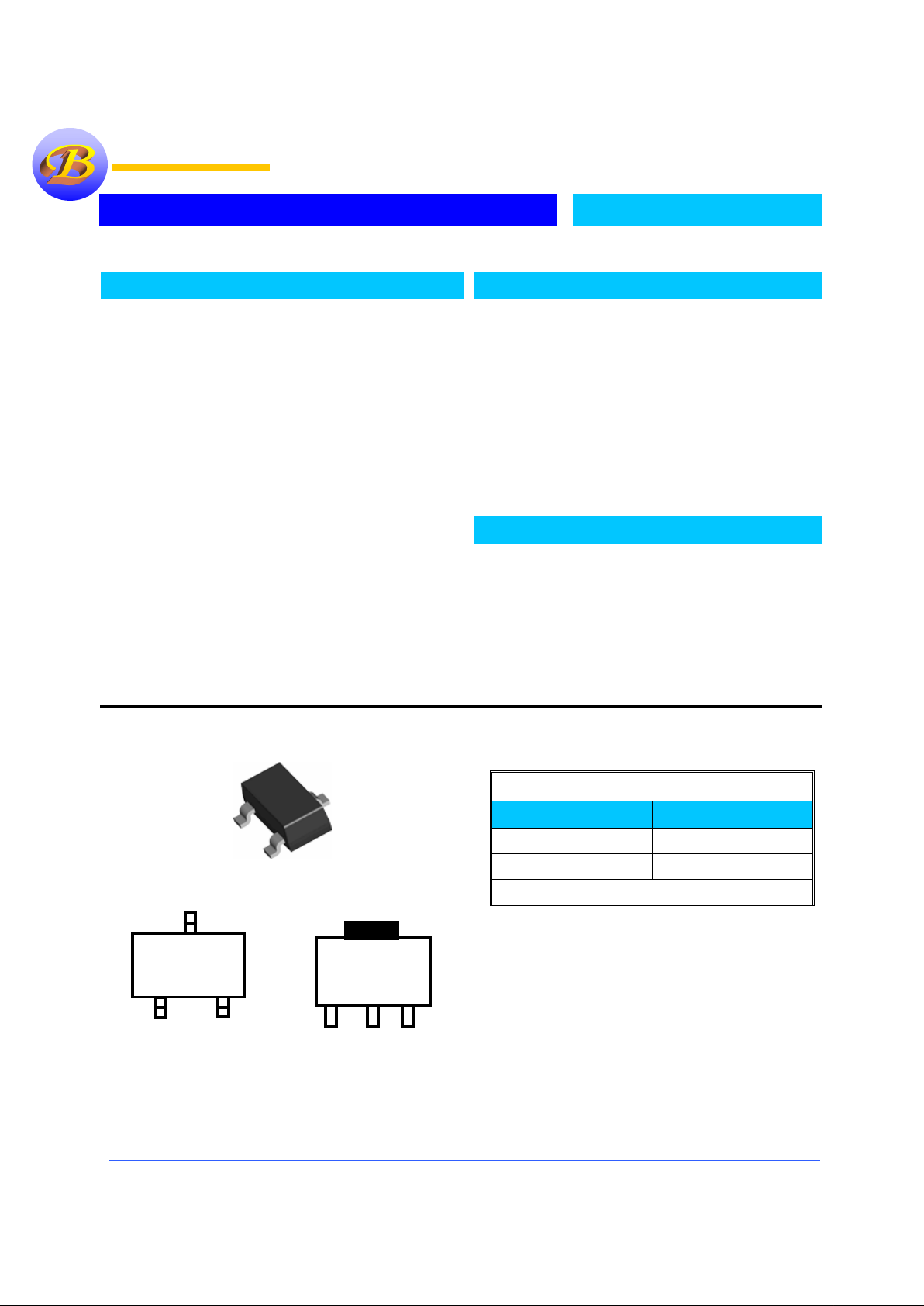
Pin Connection
Ordering Information
-40°°°°C to +125°°°°C
Package Part No.
SOT-23 B4250CK3 -X.X
SOT-89 B4250CR-X.X
X.X = Fixed Output Voltages from 2.0V to 6.0V
Description
The B4250 series are a group of positive output voltage,
three-pin r egulators, which pr ovide a high current eve n
when the input/output voltage differential is small. Low
power consumption and high accuracy is achieved
though CMOS and programmable fuse technologies.
Output voltage: 2.0V to 6.0V in 0.1V increments.
The B4250 consists of a high-precision voltage
reference, an error correction circuit, and a current
limited output driver.
Available in SOT-23 (150mW) and SOT-89 (500mW)
packages minimizing the usage of board real state.
Features
• Maximum output current: 250 mA.
• Highly accurate: Output voltage +/- 2%. (1%)
• CMOS low power consumption.
• Small input/output differential:
0.38V at 160mA (Vout=3.3V)
0.12V at 100mA (Vout=5V)
• Pin-to-Pin Improve XC62FP/XC6201
Applications
• Battery Powered Equipment
• Notebook PC, Palmtops, PDA
• Portable Cameras and Video Recorders
• Reference Voltage Sources
SOT-23-3 (K3)
Top View
V
out
V
in
V
ss
3
2
1
Top View
SOT-89 (R)
1
2
3
Vss Vin Vout
2
Vin
Bay Linear
Bay LinearBay Linear
Bay Linear
Inspire the Linear Power
Inspire the Linear PowerInspire the Linear Power
Inspire the Linear Power

Bay Linear, Inc
2418 Armstrong Street, Livermore, CA 94550 Tel: (925) 606-5950, Fax: (925) 940-9556 www.baylinear.com
B4250
Absolute Maximum Ratings
Parameter Symbol Ratings Units
Input Voltage VIN 12 V
Output Current I
OUT
500 mA
Output Voltage V
OUT
V
SS
-0.3 to VIN 0.3 V
Continual Total
Power Dissipation
SOT-23
SOT-89
Pd
150
500
mW
Operating Ambient Temperature T
OPR
-30 to 80
°
C
Storage Temperature T
STG
-40 to 125
°C
Electrical Characteristics (Ta = 25
°°°°
C, V
IN
= V
OUT +
1V; unless otherwise noted)
Parameter Conditions MIN TYP MAX UNIT
3.3V IO = 40mA, VIN = 4.3V 3.234 3.300 3.366
Output Voltage
5.0V I
O
= 40mA, VIN = 6.0V 4.900 5.000 5.100
V
3.3V IO = 40mA, 4.3V<VIN<10V
Line Regula tion ∆V
OUT
/∆VIN-V
OUT
5.0V I
O
= 40mA, 6.0V<VIN<10V
0.2 0.3 %V
3.3V VIN 4.3V, 1mA < IO < 80mA 45 90
Load Regulation
5.0V VIN 6V, 1mA < I
O
< 100mA 40 80
mV
3.3V VIN = 4.3V 1.0 2.9
Current Consumption
5.0V V
IN
= 6.0V 2.0 4.5
µ
A
3.3V IO = 160 mA 0.4 0.7
0.12 0.3
Dropout Voltage
5.0V
I
O
= 100 mA
200 mA
0.38 0.6
V
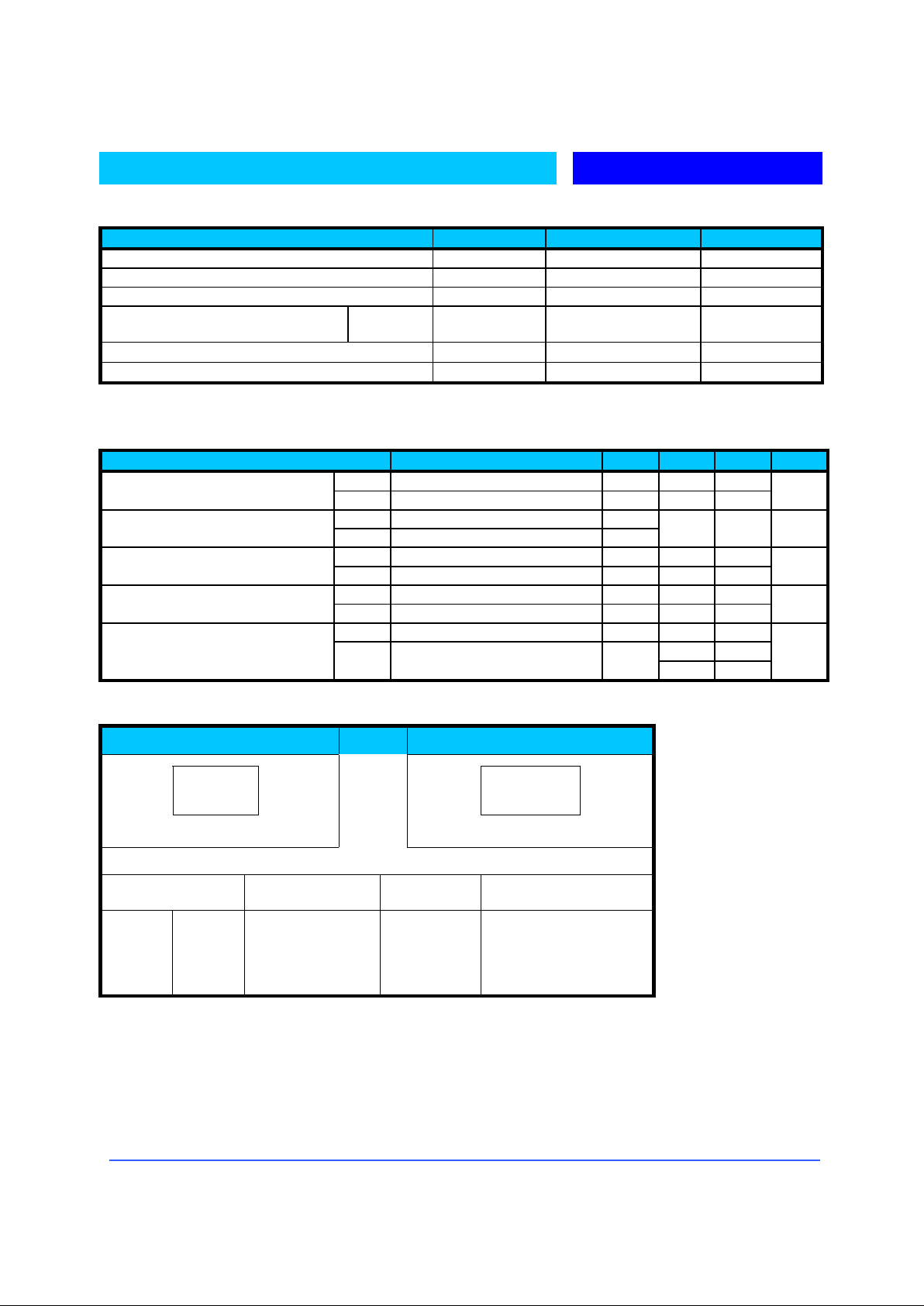
Marking Format
SOT-23
SOT-89
CXWW
B4250
XZYWW
C = B4250
Variables
X = Voltage Codes
Z = Production
Code
Y = Year WW = Work Week Code
B = 2.0 F = 3.3
01 = 2001 SOT-23 = 01 to 99
C = 2.5 G = 3.5
02 = 2002 SOT-89 = 01 to 52
D = 2.8 H = 5.0
03 = 2004
E = 3.0
etc
 Loading...