BAYLI B4151CK5-4.1, B4151CK5-4.0, B4151CK5-3.9, B4151CK5-3.8, B4151CK5-3.7 Datasheet
...
Bay Linear, Inc
2478 Armstrong Street, Livermore, CA 94550 Tel: (925) 606-5950, Fax: (925) 940-9556 www.baylinear.com
150 mA CMOS Low Dropout LDO
B4151
ON/OFF
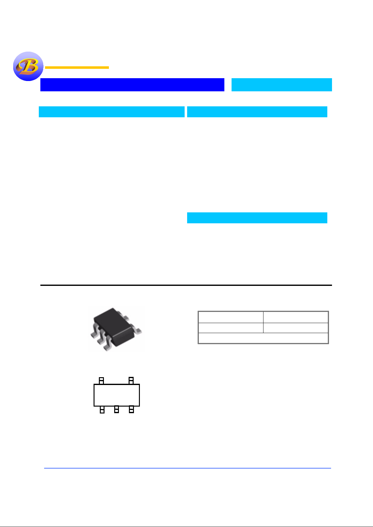
Pin Connection
Ordering Information
Package Part No.
SOT-25 B4151CK5 -X.X
X.X = Fixed Output Voltages from 2.0V to 6.0V
Description
The B4151 series are a group of positive output voltage,
five-pin regulators, which provide a high current even
when the input/output voltage differential is small. Low
power consumption and high accuracy is achieved
though CMOS and programmable fuse technologies.
Output voltage: 2.0V to 6.0V in 0.1V increments.
The B4151 consists of a high-precision voltage
reference, an error correction circuit, and a current
limited output driver. Key features include a Shutdown
Pin that reduces supply current. With good transient
responses, output remains stable even during load
changes.
The ON/OFF pin enables the output to be turned off,
resulting in reduced power consumption. Provided in
SOT-25 (150mW) packages minimizes the usage of
board real state.
Features
• Maximum output current: 150 mA.
• Highly accurate: Output voltage +/- 2%(1%)
• Shutdown Supply Current 1µµµµA
• Ground Current of Less than 20µµµµA
• CMOS low power consumption.
0.20V at 160mA
0.38V at 80mA
• Small input/output differential:
• Shut Down Mode for Power Savings
• Improve pin-to-pin XC62GR-XX
• Pin-to-Pin Low Power to Bipolar LDO’s
Applications
• Battery Powered Equipment
• Notebook PC, Palmtops, PDA
• Portable Cameras and Video Recorders
• Reference Voltage Sources
• Cellular / GSM / PCS Phones
Bay Linear
Bay LinearBay Linear
Bay Linear
Inspire the Linear Power
Ins
p
ire the Linear PowerInspire the Linear Power
Ins
p
ire the Linear Power
SOT-25 (K5)
Top View
ON/OFF
V
IN
V
SS
32
1
45
V
out
NC
SOT-25 (K5)
Top View
ON/OFF
V
IN
V
SS
32
1
45
V
out
NC

Bay Linear, Inc
2478 Armstrong Street, Livermore, CA 94550 Tel: (925) 606-5950, Fax: (925) 940-9556 www.baylinear.com
B4151
Absolute Maximum Ratings
Parameter Symbol Ratings Units
Input Voltage VIN 12 V
Output Current I
OUT
500 mA
Output Voltage V
out
VSS -0.3 to VIN 0.3 V
CE Output Voltage V
OUT
V
SS
-0.3 to VIN 0.3 V
Continual Total Power Dissipation SOT-25
SOT-89
Pd
300
500
mW
Operating Ambient Temperature T
OPR
-30 to 80
°
C
Storage Temperature T
STG
-40 to 125
°C
Electrical Characteristics (T
a
= 25
°°°°
C, V
IN
= V
OUT +
0.5V; unless otherwise noted)
Parameter Conditions MIN TYP MAX UNIT
IO = 1mA -1.4% - +1.4%
Output Voltage Accuracy
I
O
= 0 to 40mA -2% - +2%
V
Line Regulation ∆V
OUT
/∆VIN-V
OUT
I
O
= 40mA,
(V
OUT
+ 0.1V)<VIN<10V
0.2 0.3 %/V
Load Regulation
VIN=V
out
+1V
1mA < I
O
< 80mA C
OUT
= 1µF
0.04 %/mV
Maximum Output Current 150
Current Limit 1000
mA
CE input voltage High 1.5 V
CE input voltage Low
0.25 V
CE input voltage High VCE=V
IN
1.0
µ
kA
CE input voltage Low VCE=V
SS
-0.2 -0.05 0
µ
kA
Input Stability ∆V
out
/∆T
opr .
. V
out
I
out
=40mA, 4V≤V
in
≤
10V
0.2 0.3
%/V
Input Voltage 10.0 V
Ground Pin Cur rent
V
in=Vce=Vout
+1V
V
in=Vout
+1V, Vce=V
ss
19
0.1
µ
A
IO = 100mA 200 395
Dropout Voltage
I
O
= 150 mA
380 770
mV
Output Voltage Temp.
±
100
°
C
Marking Format
SOT-25
EXWW
E = B4151
Variables
X = Voltage Codes WW = Work Week Code
B = 2.0 F = 3.3
SOT-25 = 01 to 99
C = 2.5 G = 3.5
D = 2.8 H = 5.0
E = 3.0
SERIES CE VOLTAGE
OUTPUT
B4151R H L ON
OFF
B4151P H L OFF
ON
 Loading...