BAYLI B3845P, B3845M, B3845AP, B3845AM, B3845A1P Datasheet
...
Bay Linear, Inc
2418 Armstrong Street, Livermore, CA 94550 Tel: (925) 606-5950, Fax: (925) 940-9556 www.baylinear.com
Current Mode PWM Controller
B3842/43/44/45A&A1
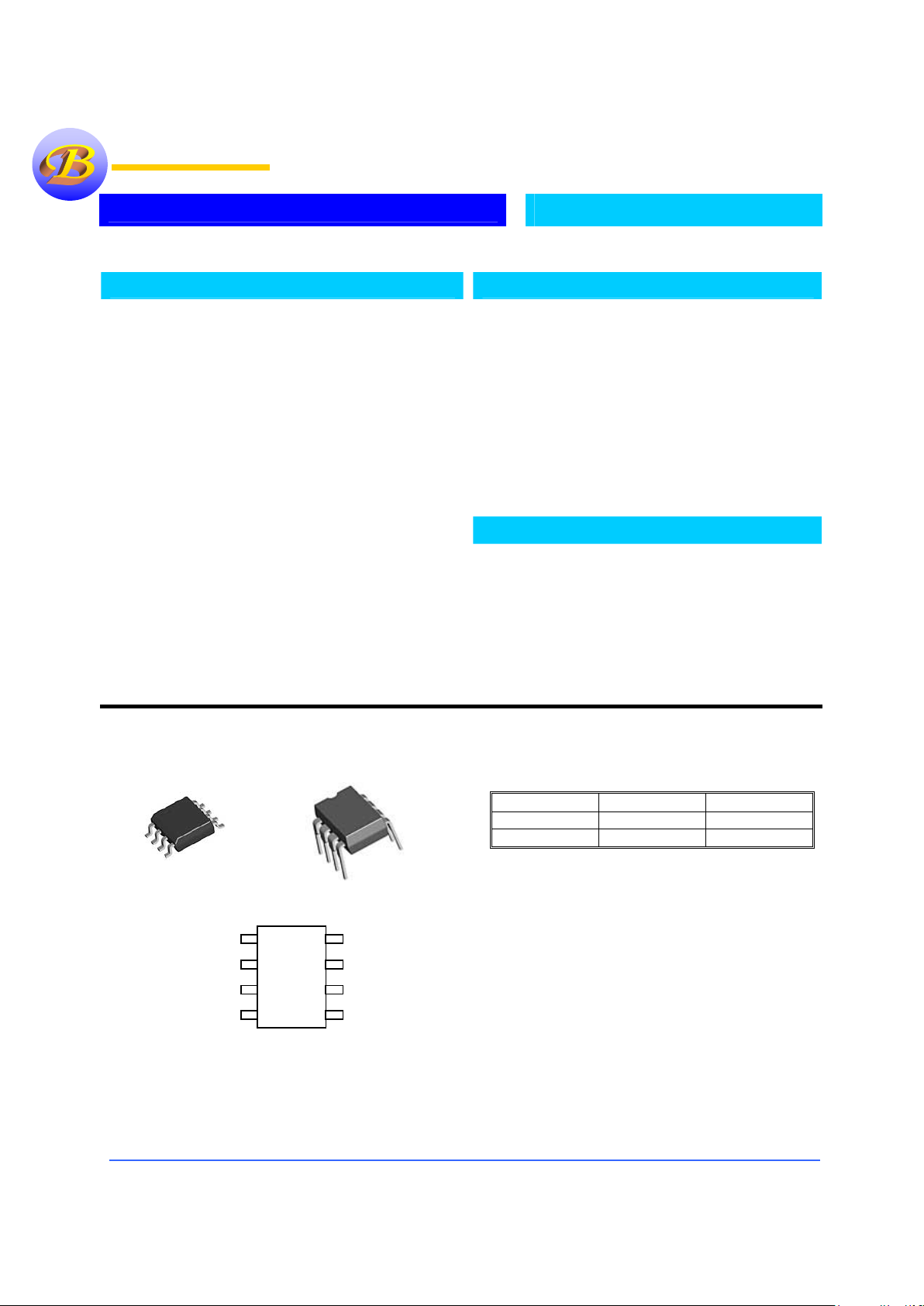
Pin Connection
Ordering Information
Devices Package Temp.
B384X(Z)M SO-8
0 °C to 70 °C
B384X(Z)P 8-DIP
0 °C to 70 °C
Z=A ON Semi Z=A1 Fairchild & Samsung
Description
The Bay Linear B3842/43/44/45 are fixed frequency currentmode PWM controller. These devices are designed for OffLine and DC-to-DC converter applications with minimum
external components. The B3842 family Feature a trimmed
oscillator for precise duty cycle control, a temperature
compensated reference, high gain error amplifier, current
sensing comparator, and a high current totempole output.
Ideally suited for driving a power N-Channel MOSFET’s. It is
low when is on off stage. Protection circuitry includes built in
under-voltage lockout and current limiting.
Major differences between members of these series are the
UVLO thresholds and maximum duty-cycle ranges. Typical
UVLO thresholds of 16V (on) and 10V (off) on the B3842 and
B3844 devices make them ideally suited to off-line
applications. These corresponding typical thresholds for the
B3842 and B3845 devcies are 8.4V (on) and 7.6V (off). The
B3842 and B3843 devcies can operate to duty cycles
approaching 100%. A duty-Cycle range of 0 to 50% is
obtained by the B3844 and B3845 by the addition of an
internal toggle flip-flop, which blanks the output off every
other clock cycle. It id available in 8 pin DIP and SOIC
packages.
Features
• Low Start-Up and Operating Current
• Maximum Duty Cycle
• Operating Frequency Up to 500KHz
• Under voltage Lockout with Hysteresis
• Available in 8 pin SOIC
• Similar to industry Standard UC3842
Applications
• Switching Power Supply
• Monitor
2
1
3
4
8
7
6
5
8-Pin Surface Mount
Top View
COMP
ISENSE
RT/CT
GND
VCC
OUTPUT
REF
NC
2
1
3
4
8
7
6
5
8-Pin Surface Mount
Top View
COMP
ISENSE
RT/CT
GND
VCC
OUTPUT
REF
NC
Bay Linear
Inspire the Linear Power

Bay Linear, Inc
2418 Armstrong Street, Livermore, CA 94550 Tel: (925) 606-5950, Fax: (925) 940-9556 www.baylinear.com
B384X
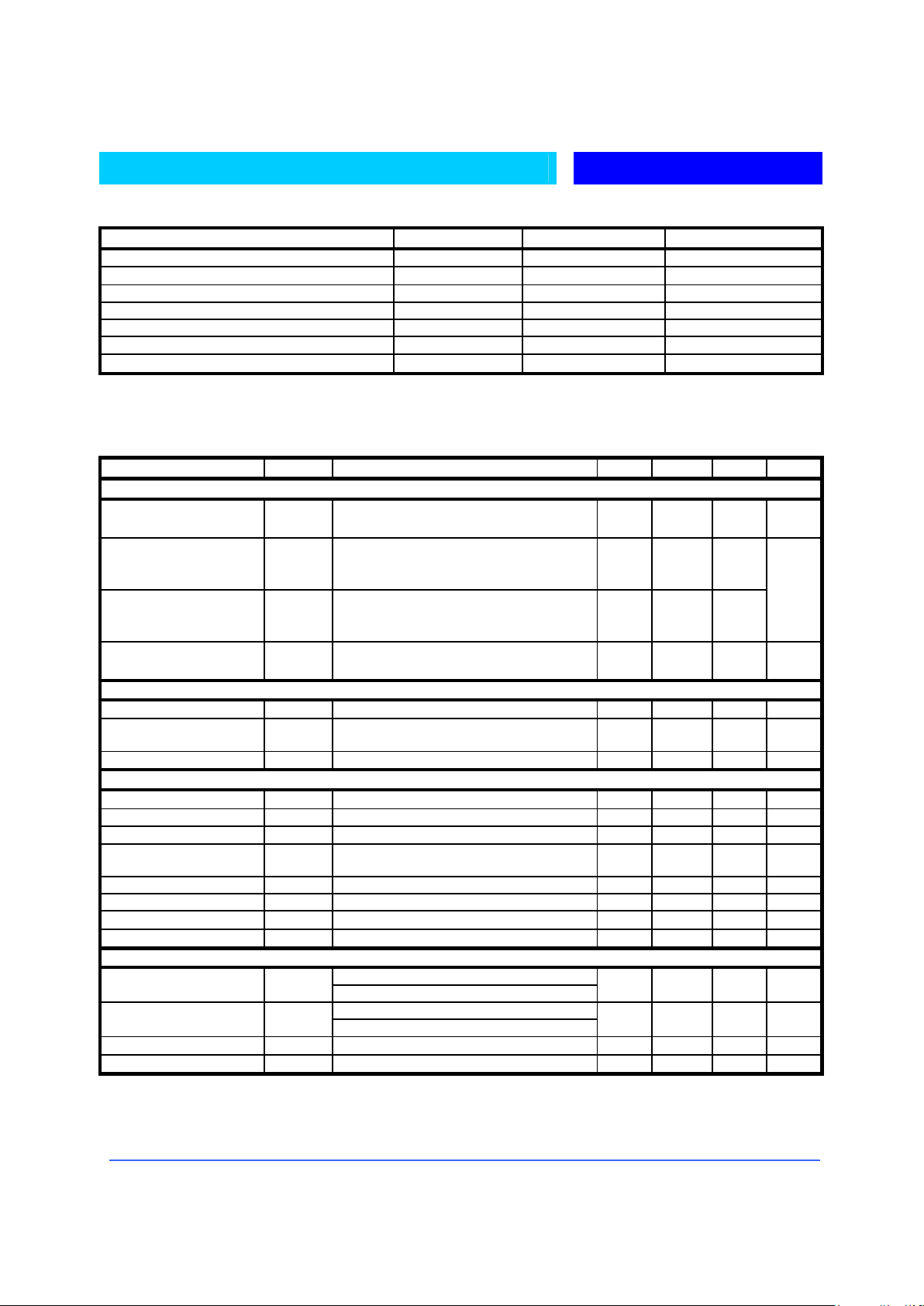
Absolute Maximum Rating
Parameter Symbol Value Unit
Supply Voltage V
CC
30 V
Output Current I
O
±1
A
Analog Input (pin 2,3) V
(ANA)
-0.3 to 6.3 V
Error Amp Output Sink Current I
SINK (E.A)
10 mA
Power Dissipation P
D
1 W
Storage Temperature Range T -65 to 150
°C
Lead Temperature (Soldering 10 Sec.) T
L
260
°C
Electrical Characteristics
(VCC = 15V;RT = 10Ω, CT = 3.3nF, TA=0 °C to +70°C, unless otherwise specified)
Parameter Symbol Conditions MIN TYP MAX UNIT
REFERENCE SECTION
Reference Voltage V
REF
TJ = 25 °C. I
REF
= 1mA
4.90 5.00 5.10 V
Line Regulation REG
(line)
12V≤VCC≤25V
- 6 20
Load Regulation REG
(LOAD)
1mA≤I
REF
≤20mA
T= 25 °C
- 6 25
mA
Short Circuit Output
Current
I
SC
T= 25 °C
- -100 -180 mA
OSCILLATOR SECTION
Oscillator Frequency f
T= 25 °C
47 52 57 KHz
Frequency Change with
Voltage
∆f/∆V
CC
12V≤VCC≤25V
- 0.05 1 %
Oscillator Amplitude V
OSC
- 1.6 - V
P-P
ERROR AMPLIFIER SECTION
Input Bias Current I
BIAS
- -0.1 -2
µA
Input Voltage V
I(E>A)
V1 =2.5V 2.42 2.50 2.58 V
Open Loop Voltage Gain G
VO
2V≤VO≤4V
65 90 - dB
Power Supply Rejection
Ratio
PSRR
12V≤V
CC
≤25V
60 70 - dB
Output Sink Current I
SINK
V2 =2.7V, V1 =1.1V 2 7 - mA
Output Source Current I
SOURCE V2
=2.3, V1=5V -0.6 -1.0 - mA
High Output Voltage V
OH
V2=2.3, RL= 15Ω to GND
5 6 - V
Low Output Voltage V
OL
V2=2.7, RL= 15Ω to pin 8
- 0.8 1.1 V
OUTPUT SECTION
I
SINK
= 20mA Low Output Voltage V
OL
I
SINK
= 200mA
- 0.08
1.4
0.4
2.2
V
S
ource
= 20mA High Output Voltage V
OH
S
ource
= 200mA
13
12
13.5
13.0
-
-
V
Rise Time t
R
TJ = 25 °C, CL=1nF (note3)
- 45 150 ns
Fall Time t
F
TJ = 25 °C, CL=1nF (note3)
- 35 150 ns
Note: Output Switch tests are performed under pulsed conditions to minimize power dissipation

Bay Linear, Inc
2418 Armstrong Street, Livermore, CA 94550 Tel: (925) 606-5950, Fax: (925) 940-9556 www.baylinear.com
B384X
Electrical Characteristics
(VCC = 15V;RT = 10Ω, CT = 3.3nF, TA=0 °C to +70°C, unless otherwise specified)
Parameter Symbol Conditions MIN TYP MAX UNIT
CURRENT SENSE SECTION
Gain G
V
(Note 1 & 2) 2.85 3 3.15 V/V
Maximum input Signal V
I(MAX) V1
= 5V (Note 1) 0.9 1 1.1 V
Power Supply Rejection
Ratio
PSRR
12V≤V
CC
≤25V
70 - dB
Input Bias Current I
BIAS
-3 -10
µA
UNDER-VOLTAGE LOCKOUT SECTION
B3842/B3844 14.5 16 17.5
Start Threshold V
TH(ST)
B3843/B3845 7.8 8.4 9
V
B3842/B3844 8.5 10 11.5
Min-Operating Voltage
(after Turn On)
V
OPR(MIN)
B3843/B3845 7.0 7.6 8.2
V
PWM SECTION
B3842/B3843
Max Duty Cycle D(MAX)
B3844/B3845
95
47
97
48
100
50
%
Min Duty Cycle D (MIN) - - 0 %
TOTAL STANDBY CURRENT
B3842A/43A/44A/45A - 0.17 0.3
Start-Up Current I
ST
B3842A1/43A1/44A1/45A1 0.45 1
mA
Operating Supply Current I
CC(OPR) V3=V2
=ON - 14 17 mA
Zener Voltage V
Z
I
CC
30 38 - V
Block Diagram
 Loading...