BAYLI B3540K4, B3520K4 Datasheet

Bay Linear, Inc
2418 Armstrong Street, Livermore, CA 94550 Tel: (925) 606-5950, Fax: (925) 940-9556 www.baylinear.com
N-CHANNEL DMOS FET SWITCH
B3520/B3540
High Gain Level Shifter
Series
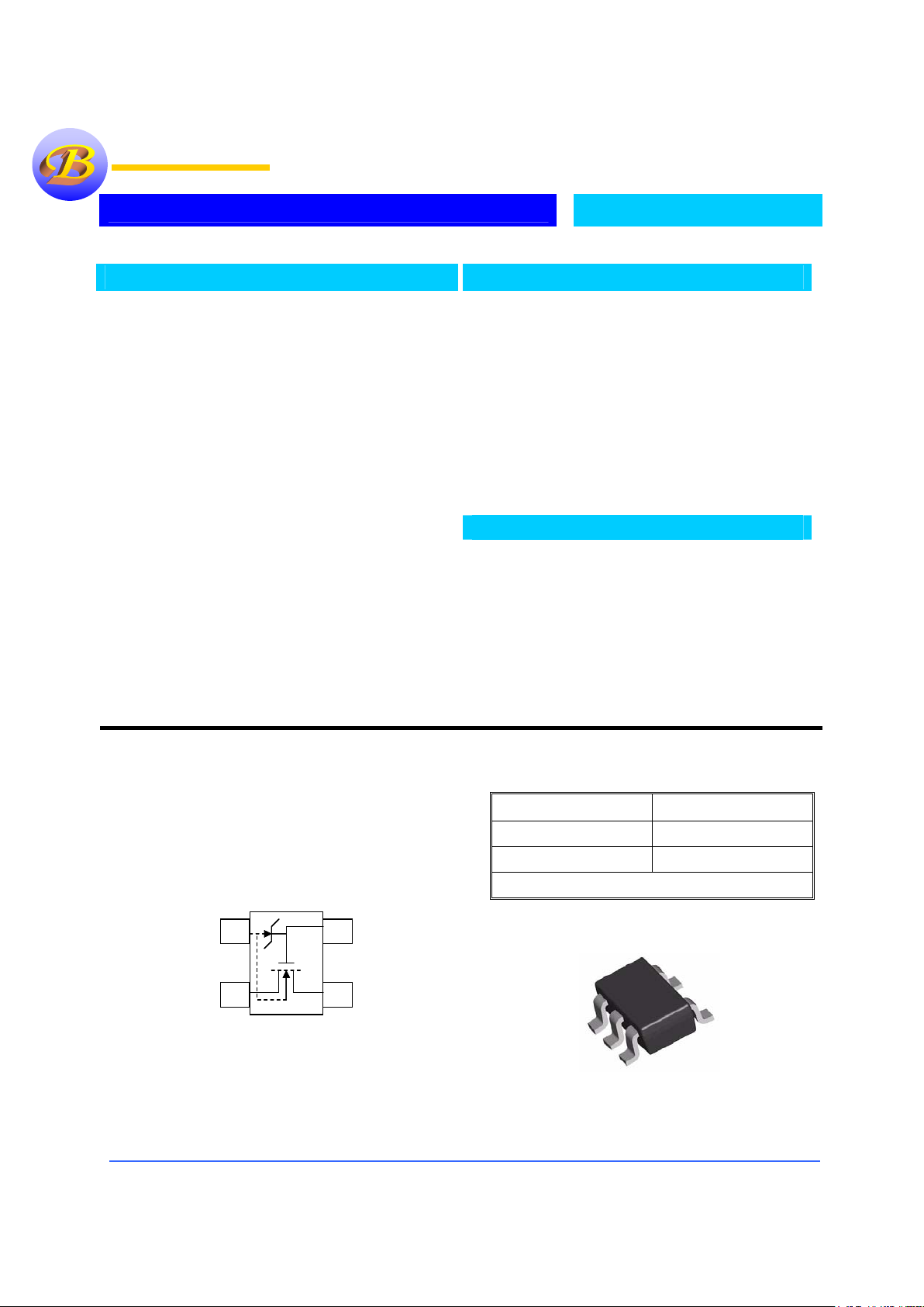
Pin Connection
Ordering Information
Package Part No.
SOT-143 B3520K4 -X.X
SOT-143 B3540K4-XX
Description
The B3520 series consists of enhancement-mode
MOSFETs designed for high speed low-glitch switching
in audio, video, and high-frequency wireless
applications. The CT3520 is optimized as a high speed
driver. With a source feedback resistor it can be uses as
a high speed LED Driver.
The B3520 series uses Bay Linear ULTRA REL DMOS
Process for reliability and robust performance.
These MOSFETs utilize lateral construction to achieve
low capacitance and ultra-fast switching speeds. An
integrated Zener diode provides ESD protection.
Features
• Low capacitance – 0.3pF typical
• Low threshold – <1.5V max
• Fast switching – ton<1ns
• CMOS and TTL Compatible Input
Application
• LED Drivers
• Level Shifting
• Switch Drivers
• VHF/UHF Amplifiers
Bay Linear
Inspire the Linear Power
2
14
3
2
14
32
14
3
SOT-143 Package
Lead Code Identification
(top view)
Body
Substrate
Source
Gate
Drain

Bay Linear, Inc
2418 Armstrong Street, Livermore, CA 94550 Tel: (925) 606-5950, Fax: (925) 940-9556 www.baylinear.com
B3520/B3540
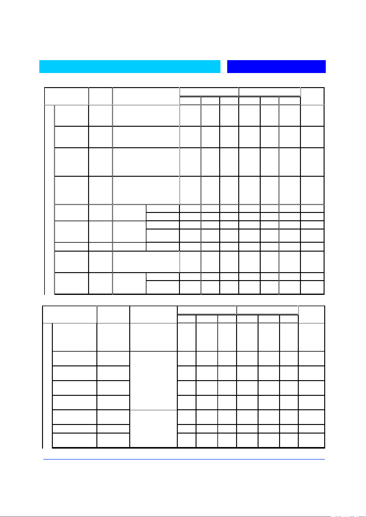
Electrical Specifications (TC = +25°C unless otherwise noted)
B3520 B3540
Parameter Symbol Test Conditions
Min Typ Max Min Typ Max
Units
Drain-Source
Breakdown
Voltage
BVDS
ID=1 µA
VGS=VBS=0
15 25 15 25 V
Source-Drain
Breakdown
Voltage
BVSD
IS=50 nA
VGD=VBD=-5
10 15 V
Drain-
Substrate
Breakdown
Voltage
BVDB
ID=50 nA, VGB=0
Source Open
10 15 V
Source-
Substrate
Breakdown
Voltage
B
VSB
I
D
=10 µA, VGB=0
Drain Open
10 15 V
VDS=10V 1 50 nA
Drain-Source
Leakage
I
D (OFF
)
V
GS/BS
=-5
V
GS/BS
=0
V
DS
=15V 0.1 1 µA
VDS=10V 1 50 nA
Source -
Drain
Leakage
IS
(OFF
)
V
GD/BS
=-5
V
GS/BS
=0
V
DS
=15V 0.1 1 µA
Gate Leakage I
GBS
V
DB/SB
= 0 VGS=20V 1 10 1 10 µA
Gate
Threshold
Voltage
V
GS
(th)
V
DS=VGS
ID=1 µA
V
SB
=0
0.3 0.7 1.5 0.3 0.7 1.5 V
VGS=2.4V 140 175 140 175 Ohm
STATIC
Drain-Source
ON
Resistance
r
DS (ON)
ID=1 mA
V
SB
= 0V
V
GS
=4.5V 40 60 40 60 Ohm
B3520 B3540
Parameter Symbol Test Conditions
Min Typ Max Min Typ Max
Units
Common-Source
Forward
Transconductance
gfS
V
DS
= 10V
I
D
= 20mA
f = 1MHz, VSB=0
Pulsed
14 18 14 18 V
Gate Node
Capacitance
C(gs+gd+gb) 4.5 6.0 4.5 6.0 pF
Drain Node
Capacitance
C(gd+db) 2.0 3.0 2.0 3.0 pF
Source Node
Capacitance
C(gs+sb) 5.5 7.0 5.5 7.0 pF
Reverse Transfer
Capacitance
C(dg)
V
DS
= 10V
V
GS=VBS
= -15V
f = 1MHz
0.3 0.5 0.3 0.5 pF
Turn On Delay
Time
td(on) 0.7 1.0 0.7 1.0 ns
Rise Time tr 0.8 1.0 0.8 1.0 ns
DYNAMIC
Turn Off Delay
Time
Td(off)
V∞= 10V
VG(on)= 10V
R
L
= 680 Ω
R
G
= 51Ω
C
L
= 1.5pF
1.5 1.5 ns
 Loading...