BAYLI B29153T-ADJ, B29153S-ADJ, B29153S-5, B29153S-3.3, B29151S-ADJ Datasheet
...
Bay Linear, Inc
2478 Armstrong Street, Livermore, CA 94550 Tel: (925) 989-7144, Fax: (925) 940-9556 www. baylinear.com
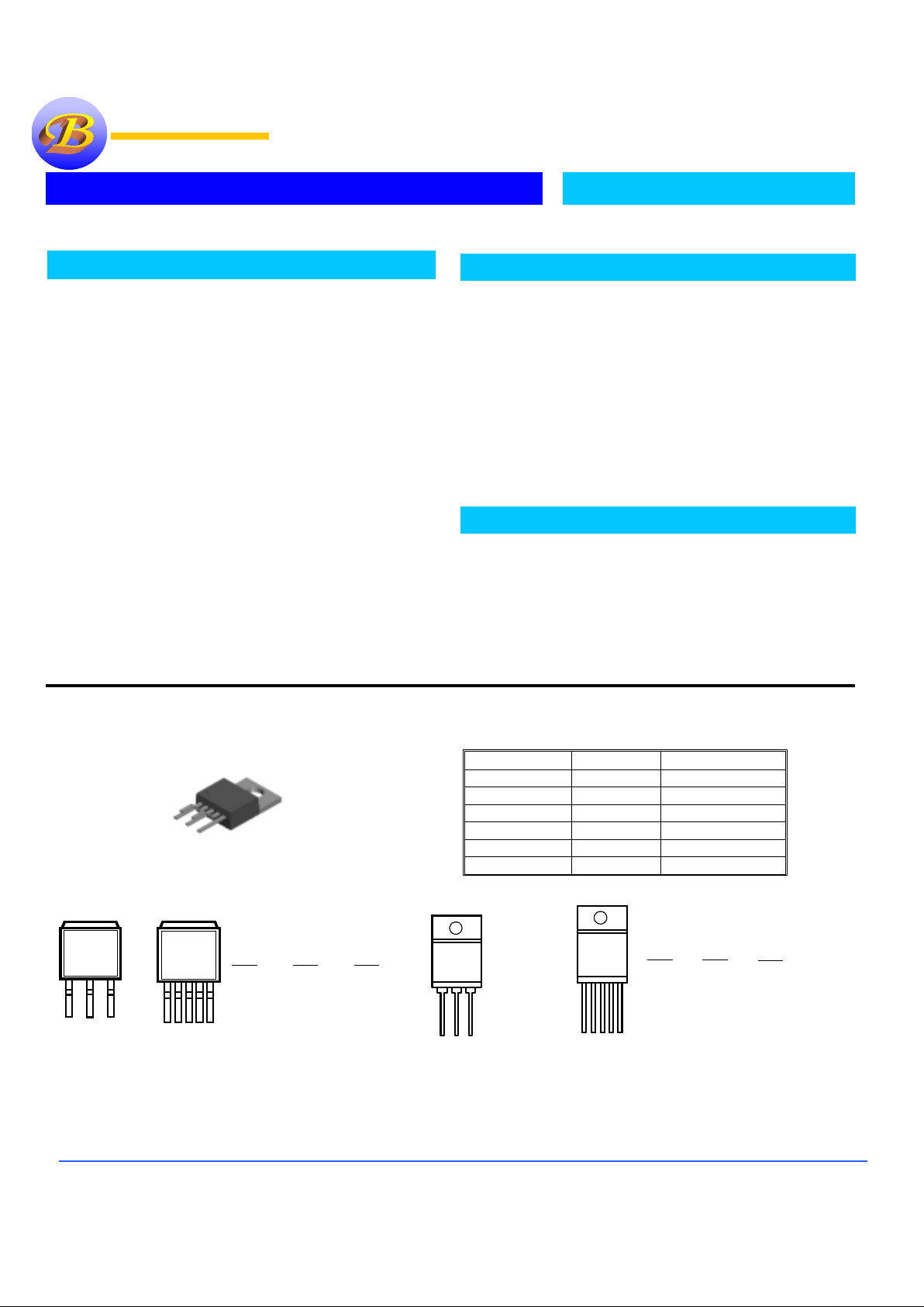
TO-220-5 Package
Top View
BAY
B29151/52/53
12345
OUTPUT
GND
FLAG
1)
3)
4)
5)
2)
INPUT
ENABLE
OUTPUT
GND
ADJUST
1)
3)
4)
5)
2) INPUT
ENABLE
OUTPUT
GND
ADJUST
1)
3)
4)
5)
2) INPUT
FLAG
B29151
B29152
B29153
1.5A High Current Low Dropout
B29150
Voltage Regulator Adjustable & Fix Output
Preliminary Information
Pin Connection
Ordering Information
Devices Package Temp.
B29150T TO-220-3
-40 °C to 125 °C
B29151/2/3T TO-220-5
-40 °C to 125 °C
B29150S TO-263-3
-40 °C to 125 °C
B29151/2/3S TO-263-5
-40 °C to 125 °C
B29150J LPDD-3
-40 °C to 125 °C
B29151/2/3J LPDD-5
-40 °C to 125 °C
Description
The Bay Linear B29150 is a 1.5A high accuracy, low dropout
voltage regulator with only 350mV(Typ.)@ 1.5A). The B29150 is
designed for low voltage a application that requires lower dropout
voltage and faster transient response. This device is an excellent
choice for use in powering low voltage microprocessor that require
a lower dropout, faster transient response to regulate from +2.5V to
3.8V supplies and as a post regulator for switching supplies
applications.
The B29150 offers full protection against over-current faults,
reversed input polarity, reversed load insertion, and positive and
negative transient voltage. On-Chip trimming adjusts the reference
voltage to 1%. F eatures su ch as Enab le pin , Error F lag pin are also
included in the 5 pin packages
.
The B29150 is offer in a new LPDD
(Low Profile TO-263) package from 4.47 mm (DD) tickness down
to only 1.27 mm (LPDD) total tickness.
The B29150 are offered in a 3 & 5-pin TO-220 & TO-263 package
compatible with other 3 terminal regulators. For a 3A low dropout
regulator refer to the B39300 data sheet.
Features
• Adjustable & Fix Output
• 1% output accuracy @2.5V, 3.3V, @ 5.0V
• Output Current of 1.5A
• Low Dropout Voltage of 350mV @ 1.5A
• Extremely Tight Load & Line Regulation
• Reverse-battery and “Load Dump” Protection
• Zero Current Shutdown Mode (5-pin version)
• Error Flag Signal Output-of-Regulation (5-pin
version)
• Offer in TO-263, TO-220, & New Slim LPDD
•
Similar to industry Standard MIC29150
Applications
• Powering VGA & Sound Card
• LCD Monitor
• USB Power Supply
• SMPS Post Regulator
• High Efficiency ”Green” Computer System
• Adjustable Power Supply
Bay Linear
Bay LinearBay Linear
Bay Linear
Inspire the Linear Power
Ins
p
ire the Linear PowerInspire the Linear Power
Ins
p
ire the Linear Power
TO-263-3 Package
V
OUT
GND
V
IN
BAY
B29150
Front View
123
OUTPUT
TO-263-5 Package
Top View
45
BAY
B29151/52/53
321
GND
FLAG
1)
3)
4)
5)
2)
INPUT
ENABLE
GND
ADJUST
1)
3)
4)
5)
2)
INPUT
ENABLE
GND
ADJUST
1)
3)
4)
5)
2)
INPUT
FLAG
OUTPUT OUTPUT
B29151
B29152 B29153
Front View
TO-220-3 Package
BAY
B29150
V
IN
V
OUT
GND

Bay Linear, Inc
2478 Armstrong Street, Livermore, CA 94550 Tel: (925) 989-7144, Fax: (925) 940-9556 www. baylinear.com
B29150
ABSOLUTE MAXIMUM RATINGS
Lead Temp. (Soldering, 5 Seconds)................................ 260°C Input Voltage........................................................ 26V
Storage Temperature Range..............................-65° to +150°C Maximum Output Current...................................3.5A
Operating J unction Temperature Range Input Supply Voltage (Not e1) (Survival)-20V to +60V
B29150/51/52/53 Control Section............. -45°C +125°C
B29150/51/52/53 Power Transistor............-45°C +150°C
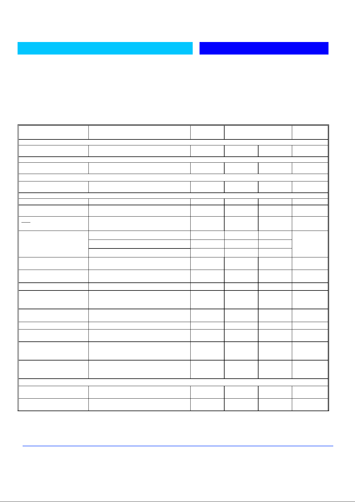
ELECTRICAL CHARACTERISTICS
(NOTE 1) at I
OUT
= 10mA, Ta=25°C, unless otherwise specified.
PARAMETER
CONDITIONS Typ B29150/51/52/53
Min Max
Units
2.5V Version
Output Voltage (Note 2)
I
OUT
= 10mA
10mA ≤I
OUT
≤1.5A, 4.75V≤V
IN
≤26V
2.5
2.5
2.475
2.450
2.525
2.550
V
3.3V Version2.
Output Voltage (Note 2)
I
OUT
= 10mA
10mA ≤I
OUT
≤1.5A, 4.75V≤V
IN
≤26V
3.3
3.3
3.267
3.234
3.330
3.366
V
5.0V Version
Output Voltage (Note 2)
I
OUT
= 10mA
10mA ≤I
OUT
≤1.5A, 5.5V≤V
IN
≤26V
5.0
5.0
4.95
4.90
5.05
5.10
V
All Voltage Options
Line Regulation
IO = 10mA, (V
OUT
+ 1V) ≤ V
IN
≤ 26V
0.06
0.5 %
Load Regulation
VIN = V
OUT
+ 5V, 10mA ≤ I
OUT
≤ I
FULLLOAD
(Note 2, 6)
0.2 1 %
∆V°
20
100
ppm/°C
∆
T
Output Voltage (Note 6)
Temperatu re Coef.
IO = 100mA
80
200
IO = 750mA
220
Dropout Voltage
I
O
= 1.5A
350
600
mV
Ground Current IO = 750mA, VIN = V
OUT
, +1V
I
O
= 1.5A
8
25
20
mA
I
GNDDO
Ground Pin Current at
Dropout
VIN = 0.5V less than specified V
OUT IOUT
= 10mA 0.9
mA
Current Limit
V
OUT
= 0V (Note 4) 1.7 1.5
A
Output Noise Voltage
(10Hz to 100kHz)
I
L
= 100mA
CL = 10µF
C
L
= 33µF
400
260
µV
RMS
Reference Voltage
1.240 1.228
1.215
1.252
1.265
V
Reference Voltage
(Note 8)`
1.203 1.277
V
Adjust Pin
Bias Current
40 80
120
nA
Reference Voltage
Temperature
Coefficient
(Note 7) 20
ppm/°C
Adjust Pin Bias
Current Temperature
Coefficient
0.1
nA/°C
Flag Output (Error Comparator) B29152/53
Output Leakage
Current
VOH = 26V 0.01 1.00
2.00
µA
Output Low
Voltage
Device set for 5V. VIN = 4.5V
I
OL
= 250µA
220 300
400
mV
 Loading...