BAYLI B2520K4, B2515K4 Datasheet

Bay Linear, Inc
2418 Armstrong Street, Livermore, CA 94550 Tel: (925) 606-5950, Fax: (925) 940-9556 www.baylinear.com
N-CHANNEL DMOS FET SWITCH
B2520/B2515
VIDEO TRANSISTOR
Series
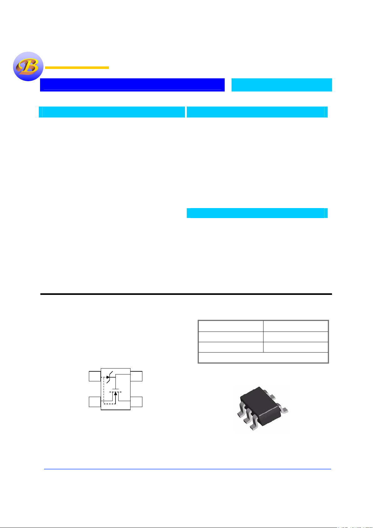
Pin Connection
Ordering Information
Package Part No.
SOT-143 B2520K4 -X.X
SOT-143 B2515K4-XX
Description
The B2520 series consists of enhancement-mode
MOSFETs designed for high speed low-glitch switching
in audio, video, and high-frequency applications. The
B2520 is optimized as a +-7V Switch driver. The B2515
is optimized as an Analog Switch with a 20V Source to
Body breakdown and low Drain Leakage.
The B2500 series uses Bay Linear ULTRA REL DMOS
Process for reliability and robust performance.
These MOSFETs utilize lateral construction to achieve
low capacitance and ultra-fast switching speeds. An
integrated Zener diode provides ESD protection.
Features
• High Input to Output Isolation – 120dB typical
• Low feed through and feedback transients
• Low Inter-electrode Capacitances
• 25V Drain-to Source breakdown for B2520
Application
• High Frequency Drivers
• Video Switches
• A to D Converters
Bay Linear
Inspire the Linear Power
2
14
3
2
14
32
14
3
SOT-143 Package
Lead Code Identification
(top view)
Body
Substrate
Source
Gate
Drain

Bay Linear, Inc
2418 Armstrong Street, Livermore, CA 94550 Tel: (925) 606-5950, Fax: (925) 940-9556 www.baylinear.com
B2520/B2515
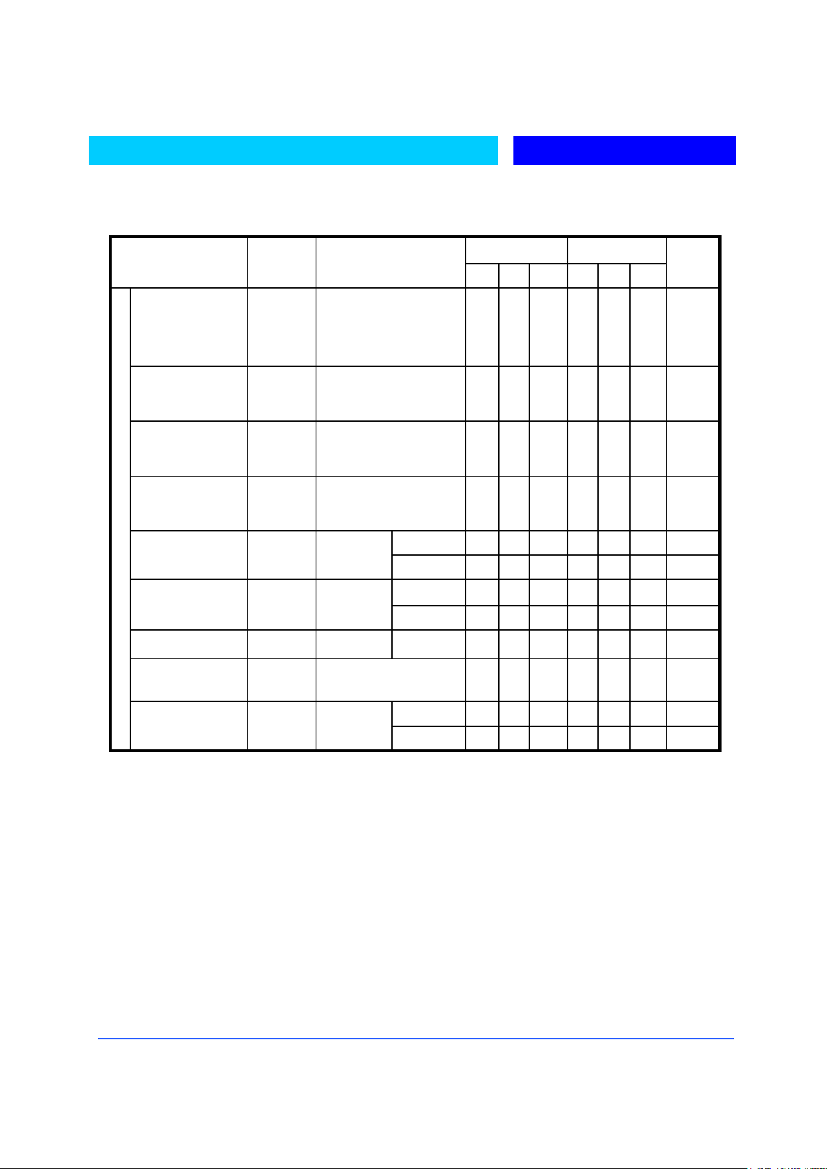
Electrical Specifications (TC= +25°C unless otherwise noted)
Ohm70507050VGS=5VID=1 mA
V
SB
= 0V
r
DS (ON)
Drain-Source
ON Resistance
V2.01.00.12.01.00.5V
DS=VGSID
=1 µA
V
SB
=0
V
GS (th)
Gate Threshold
Voltage
STATIC
V
DB/SB
= 0
V
GD/BS
=-5
V
GS/BS
=-5 nA501VDS=10V
Gate Leakage
Source - Drain
Leakage
Drain-Source
Leakage
Source-Substrate
Breakdown
Voltage
Drain-Substrate
Breakdown
Voltage
Source-Drain
Breakdown
Voltage
Drain-Source
Breakdown
Voltage
UnitsB2515B2520
Ohm45304530V
GS
=10V
µA101101V
GS
=20VI
GBS
nA501VDS=20V
nA501V
DS
=10VI
S (OFF)
nA501VDS=20V
I
D (OFF)
V2015ID=10 µA, VGB=0
Drain Open
BV
SB
V2015ID=50 nA, VGB=0
Source Open
BV
DB
V152510IS=50 nA
V
GD=VBD
=-5
BV
SD
V
2520
30
25
25
10
ID=10 µA
V
GS=VBS
=0
I
D
=50 nA
V
GS=VBS
=0
BV
DS
BV
DS
MaxTypMinMaxTypMin
Test ConditionsSymbolParameter
 Loading...