BAYLI B2076-2M, B2076-1P, B2076-1M, B2026-2P, B2026-2M Datasheet
...
Bay Linear, Inc
2418Armstrong St., Livermore CA USA 9550 Tel: (925) 606-5950, Fax: (925) 940-9556 www.baylinear.com
Dual-Channel Power Distribution Switc h
B2025/2076
Advance Information
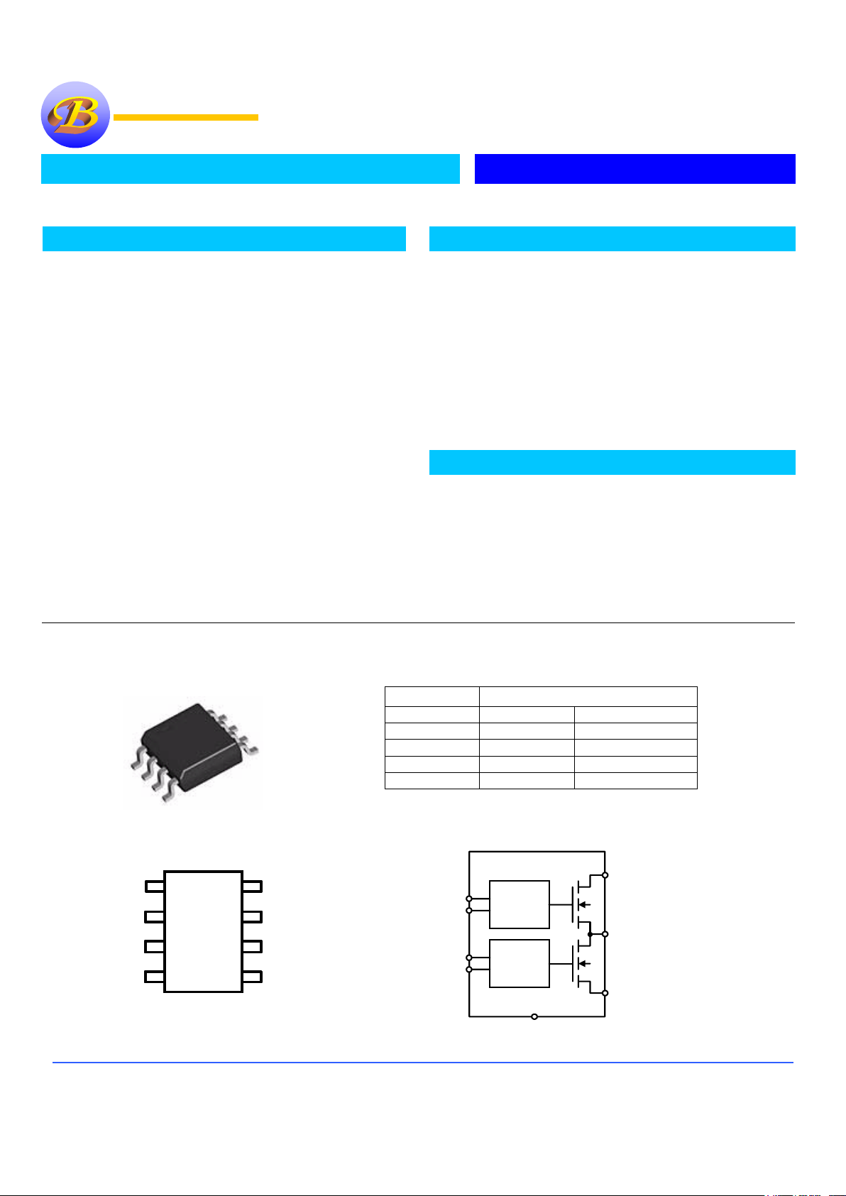
Package Information Ordering Information
Package Enable
Active High Active Low
SO-8 B2026-1M B2026-2M
SO-8 B2076-1M B2076-2M
8 DIP B2026-1P B2026-2P
8 DIP B2076-1P B2076-2P
Description
The Bay Linear B2026 & B2076 are a dual high-side power
switch recommended for general Propose self-powered and
bus-powdered universal serial for bus (USB) application
conforming to USB requirements. These devices include
thermal shutdown which in fault modes reduces the current
consumptions.
Additional features such as thermal shutdown to prevent
catastrophic switch failure from excessively high current
loads, under voltage lockout (UVLO) to ensure that the device
remains off unless there is a valid input voltage present. These
device it includes internal current limits. The 2026/76 offer a
soft-start circuit for limit the inrush current and Fault status
output flag for time over current and thermal shutdown status.
Bay Linear B2026/76 are available in 8-pin Dip and 8-pin
SOIC packages.
Features
• 2.7V to 5.5V Input
• Under voltage Lockout
• 1µµµµA Typical off-State Supply Current
• 500mA Minimum Continuous Load Current
• B2076 with Circuit Breaker Mode
• Logic Compatible Input
• Thermal Shutdown & Short Circuit pro t ection
• Pin Compatible with B2526
• Replacement for MIC2026/76
Applications
• USB Host and self-Powered Hubs
• USB Power Management
• Battery-Charger Circuits
• Hot Plug-In Power Supplies
• Bus-Powered Hubs
• Notebooks/PDA
• ACPI power distribution
Bay Linear
Bay LinearBay Linear
Bay Linear
Inspire the Linear Power
Inspire the Linear PowerInspire the Linear Power
Inspire the Linear Power
Logic
Charge
Pump
Logic
Charge
Pump
8 Out (A)
7 IN
5 Out (B)
6 GND
EN (A) 1
FLG (A) 2
FLB (B) 3
EN (B) 4
Top View
2
1
3
4
8
7
6
5
BAY
B2026/76
FLAG (B)
EN (B)
V
OUT
(A)
GND
V
IN
FLAG (A)
EN (A)
SO-8/8-DIP
V
OUT
(B)
Top View
2
1
3
4
8
7
6
5
BAY
B2026/76
FLAG (B)
EN (B)
V
OUT
(A)
GND
V
IN
FLAG (A)
EN (A)
SO-8/8-DIP
V
OUT
(B)

Bay Linear, Inc
2418Armstrong St., Livermore CA USA 9550 Tel: (925) 606-5950, Fax: (925) 940-9556 www.baylinear.com
B2026/76
ABSOLUTE MAXIMUM RATINGS OPERATING RATING
Supply Voltage…………………………………..+.6V Supply Voltage............................................... +2.7V to +5.5V
Fault Flag Voltage……………………………….+.6V
Ambient Operating Temperature.................... -40°C to +85°C
Fault Flag Current……………………………..25mA
Output Voltage……………………………………6V
Output Current……………………Internally Limited
Enable Input……………………………-0.3V to +3V
Storage Temperature………………-65°C to +150°C
Lead Temperature (Soldering 5 sec.)………….260°C
Thermal Resistance
SOIC.................................................................. 160°C/W
DIP..................................................................... 105°C/W
ELECTRICAL CHARACTERISTICS
at V
IN
= 5V, Ta=25°C, unless otherwise specified. (Note 1)
Parameters
Conditions
Typ Min Max Units
Supply Current Switch Off, OUT = Open V
ENA=VEMB
≤0.8V
Switch Off, OUT = Open V
ENA=VEMB
≥2.4V
Switch On, OUT = Open V
ENA=VEMB
≤0.8V
Switch On, OUT = Open V
ENA=VEMB
≥2.4V
0.75
0.75
100
100
5
5
160
160
µ
A
Enable Input Threshold Low to High Transition
High to Low Transition, (Note1)
1.7
1.45
0.8
2.4 V
Enable Input Current VEN = 0V to 5.5V
± 0.01 -1 1
µ
A
Enable Input Capacitance 1 pF
Switch Resistance VIN = 5V I
OUT
= 500mA, Each Switch
VIN = 3.3V I
OUT
= 500mA, Each Switch
90
100
140
170
mΩ
Output Turn-On Delay
R
L
= 10Ω, CL=1µf
1.3 5 ms
Output Turn-On Rise Time
R
L
= 10Ω, CL=1µf
1.15 4.9 ms
Output Turn-Off Delay
R
L
= 10Ω, CL=1µf
35 100
µ
s
Output Turn-Off Fall Time
R
L
= 10Ω, CL=1µf
32 100
µ
s
Output Leakage Current Each output (output disabled)
10
µ
A
Continuous Load Current Each output 0.5 A
Short Circuit Current Limit Each output (enable into load), V
OUT
= 0V 0.9 0.5 1.25 A
Current Limit Threshold
Ramped Load applied to enable output, V
OUT
≤
4.0V
1.0 1.25 A
Over current Flag Response Delay VIN=5V, apply V
OUT
=0V UNTIL FLAG LOW
V
IN
=3.3V, apply V
OUT
=0V UNTIL FLAG LOW
3.0
3.0
1.5
7.0
ms
Short Circuit Response Time V
OUT
=0V to I
OUT=ILIMIT
20 µs
Error Flag Off Current V
FLAG
= 5V
0.01 1
µ
A
UVLO Threshold VIN = Increasing
VIN = Decreasing
2.4
2.15
2.2
2.15
2.7
2.5
V
 Loading...