BAYLI B1150T-3.3, B1150T-3.0, B1150T-2.5, B1150T-1.5, B1150S-ADJ Datasheet
...
Bay Linear, Inc
2478 Armstrong Street, Livermore, CA 94550 Tel: (925) 989-7144, Fax: (925) 940-9556 www.baylinear.com
4.0A Low Dropout Voltage Regulator
B1150
Adjustable & Fix Output
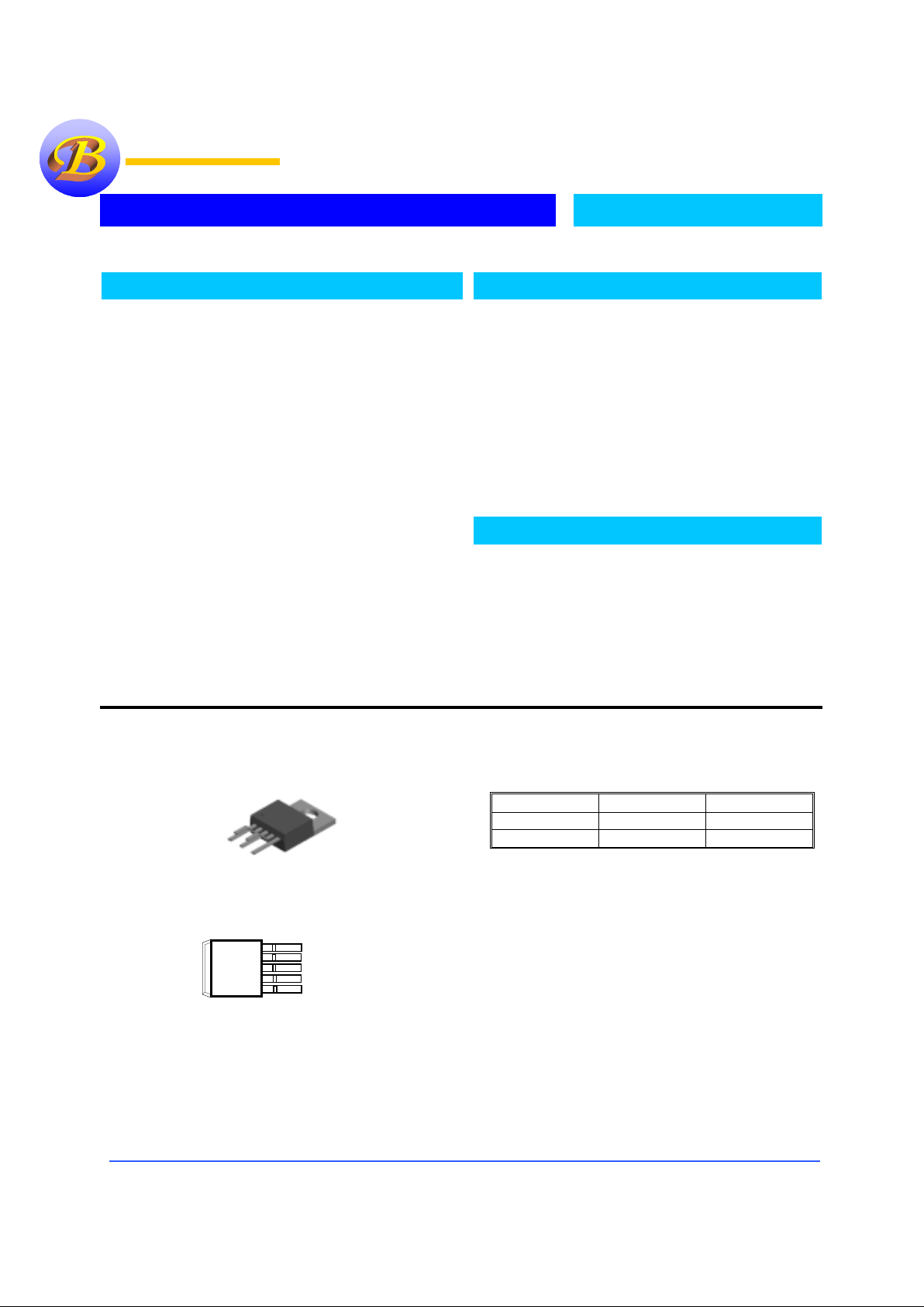
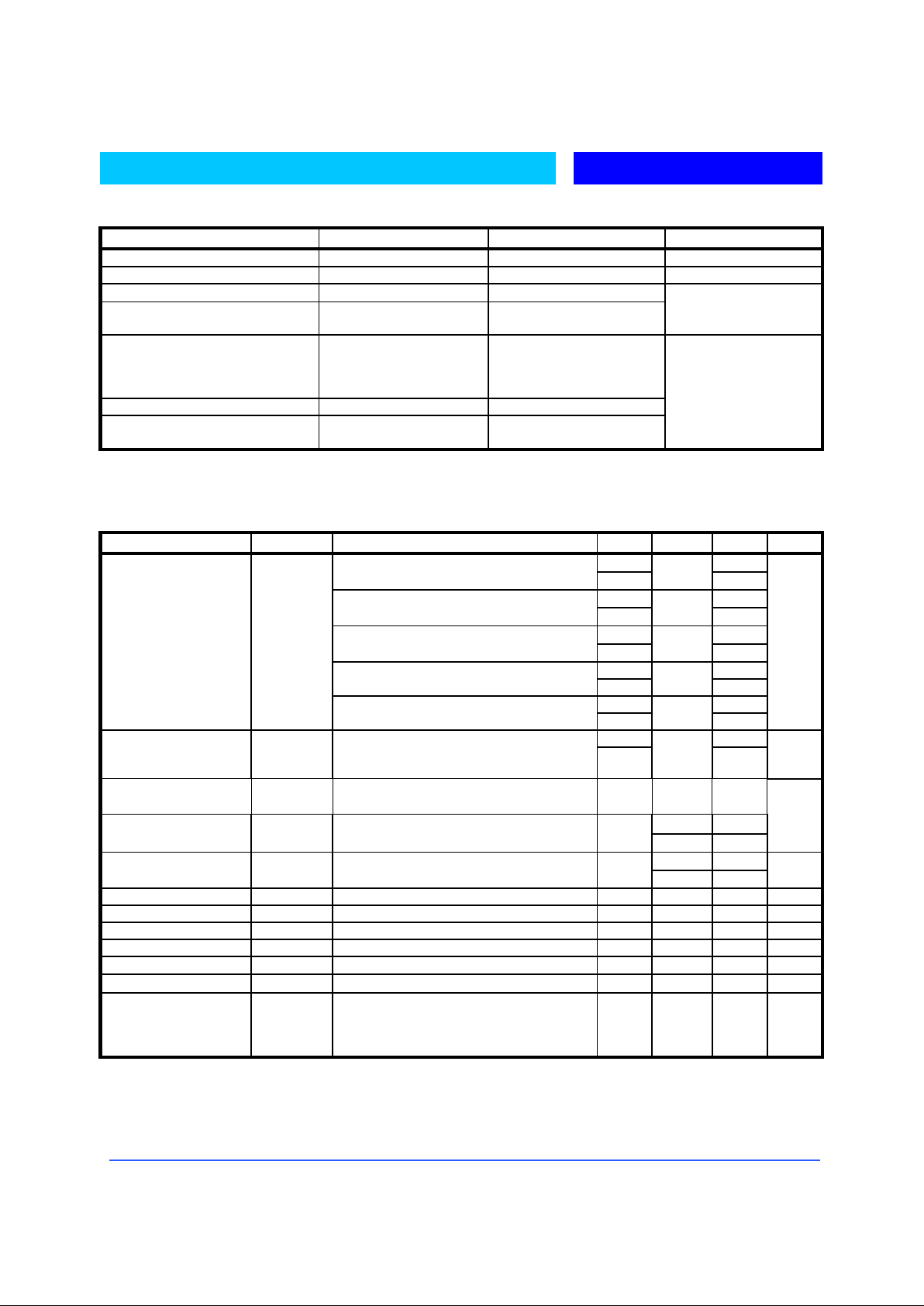
Pin Connection
Ordering Information
Devices Package Temp.
B1150T TO-220
0 °C to 70 °C
B1150S TO-263
0 °C to 70 °C
Description
The Bay Linear B1150 is Monolithic low power 4.0A
Adjustable and fixed NPN voltage regulator that are easy to
use with minimum external components. It is suitable for
applications requiring a well-regulated positive output voltage
with low input-output differential voltage requirements and
output voltage 1.5V, 2.5V, 3.0V, 3.3V, or 5V.
The B1150 Outstanding features include full power usage up
to 4.0Amp of load current internal current limiting and thermal
shutdown. Other fixed versions are also available consult with
factory.
The B1150 is offered in a 5-pin TO-220, & TO-263 packages
compatible with other 5 terminal regulators.
Features
• Adjustable Output Down to 1.2V
• Fixed Output Voltages 2.5V, 3.0V 3.3V,
and 5.0V
• Output Current of 4.0A
• Low Dropout Voltage 700mV Typ.
• Current & Thermal Limiting
• Standard 3-Terminal Low Cost TO-220,
D
2
Packages
•
Similar to industry Standard IRU1150
Applications
• 3.3V to 2.5V for Pentium Processor
• SMPS Post Regulator
• High Efficiency “Green” Computer
Systems
• High Efficiency Linear Power Supplies
• 5V to 3.XXV fro Pentium Processor
• Battery Charger
Bay Linear
Bay LinearBay Linear
Bay Linear
Linear Excellenc e
V
POWER
OUTPUT
1
2
3
4
5
V
CONTROL
ADJ/GND.
SENSE
TO-263-5 Package
V
POWERVPOWER
OUTPUT
1
2
3
4
5
V
CONTROLVCONTROL
ADJ/GND.
SENSE
TO-263-5 Package

Bay Linear, Inc
2478 Armstrong Street, Livermore, CA 94550 Tel: (925) 989-7144, Fax: (925) 940-9556 www.baylinear.com
B1150
Absolute Maximum Rating
Parameter Symbol Value Unit
Maximum Input Voltage V
IN
7 V
Power Dissipation P
O
Internally Limited W
Thermal Resistance Junction to Case
θ
JC
3
Thermal Resistance Junction to
Ambient
θ
JA
50
°
C/W
Operating Junction
Temperature Range
Control Section
Power Transistor
T
J
0 to 125
0 to 150
Storage Temperature Range T
STG
-65 to 150
Lead Temperature (Soldering 10
Sec.)
T
LEAD
260
°
C
Electrical Characteristics
(VIN = 4.75V to 5.25V; IO = 10mA to 4.0Amp, unless otherwise specified)
Parameter Symbol Conditions MIN TYP MAX UNIT
1.485 1.515 V
CONT
=4V, V
PWR
=2V
V
CONT
=3V, V
PWR
=2.3V, I
LOAD
=10mA to 4A
1.475
1.5
1.525
2.475 2.525 V
CONT
=5V, V
PWR
=3.3V
V
CONT
=4V, V
PWR
=3.3V, I
LOAD
=10mA to 4A
2.460
2.5
2.540
2.970 3.030 V
CONT
=5.5V, V
PWR
=3.5V
V
CONT
=4.5V, V
PWR
=3.8V, I
LOAD
=10mA - 4A
2.950
3.0
3.050
3.267 3.333 V
CONT
=5.8V, V
PWR
=3.8V
V
CONT
=4.8V, V
PWR
=4.1V, I
LOAD
=10mA - 4A
3.247
3.3
3.353
4.950 5.050
Output Voltage V
O
V
CONT
=7.5V, V
PWR
=5.5V
V
CONT
=6.5V, V
PWR
=5.8V, I
LOAD
=10mA- 4A
4.920
5.0
5.080
V
1.238 1.262 Reference Voltage V
ref
V
CONT
=2.75V, V
PWR
=2V, I
LOAD
=10mA
V
CONT
=2.7V, to 12V
V
PWR
=3.3V to 5.5V, I
LOAD
=10mA to 4A
1.230
1.250
1.270
V
Line Regulation (1) REG
(line)
IO = 10mA, VIN =5V, T= 25 °C
0.04 0.2
0.08 0.40 Load Regulation (1) REG
(LOAD)
IO = 10mA, VIN =5V, T= 25 °C
%
0.55 0.70 Dropout Voltage V
PWR-VOUT VCONT=VOUT
+2.5V, I
LOAD
=4A
V
Minimum load Cu rrent I
min
5 10 mA
Current Limit I
S
(Vin-V
out
)=3V 4 5 A
Ground Pin Current I
Q
VIN =5V 5 10 mA
Temperature Stability T
S
IO = 10mA, VIN =5V 0.5 %
Thermal Regulation
T= 25 °C, 30ms pulse
0.003 %/W
Ripple Rejection R
A
T= 25 °C, VIN =5V
60 75 dB
Thermal Resistance - TO-220 Junction to Tab
Junction to Ambient
DD Package Junction to Tab
Junction to Ambient
3.0
60
3.0
60
3.0
60
3.0
60
°
C/W
Note:
Output Switch tests are performed under pulsed conditions to minimize power dissipation
 Loading...