BAYLI B1121-Z-5.0, B1121-Z-3.3, B1121-Z-3.0, B1121-R-5.0, B1121-R-3.3 Datasheet
...
Bay Linear, Inc
2478 Armstrong Street, Livermore, CA 94550 Tel: (925) 989-7144, Fax: (925) 940-9556 www.baylinear.com
150mA Low Dropout Voltage Regulator
B1121
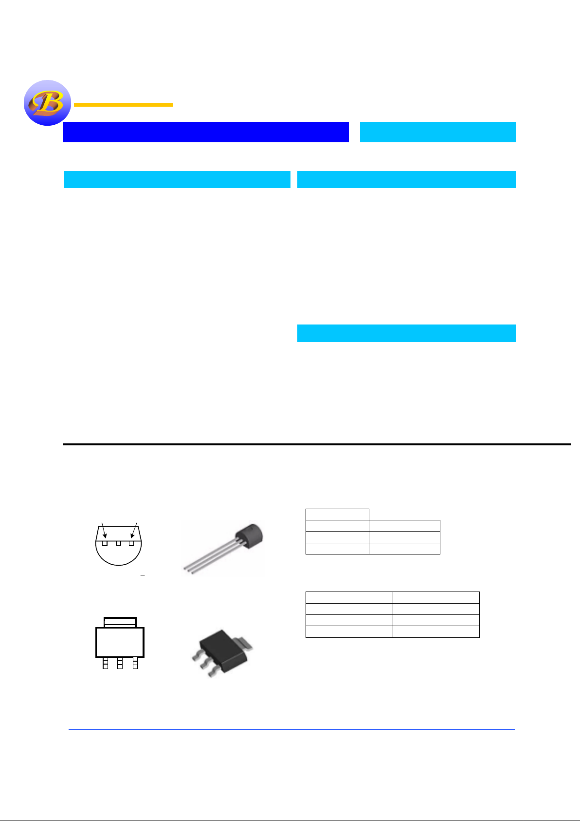
Pin Connection
TO-92 (Z)
Ordering Information
Package
1%
SOT-223
B1121-R-XX
TO-92
B1121-Z-XX
“XX” Voltage Selection Guide
Vout XX Code
5.0V
5
3.3V
3.3
3V
3
Description
The Bay Linear B1121 is a low power voltage regulator.
This device is an excellent choice for use in batterypowered applications such as cordless telephones, radio
control systems, and portable computers. The B1121
features very low quiescent current and very low
dropout voltage of 0.40 volts. This includes a tight
initial tolerance of ± 1% max, and very low output
temperature coefficient, making the B1121 useful as a
low-power voltage reference.
The B1121 feature low quiescent current ( 75µA Typ.)
and low dropout of 40mV at light loads 400mV (typ.) at
150mA.
The Bay Linear B1121 is available in fixed voltages of 3.0V,
3.3V, and 5.0V in a SOT-223 and TO-92 packages.
Features
•
1% Output Accuracy @ 3.0V, 3.3V, 5.0V
•
Very Low Quiescent Current
•
0.40V Low Dropout Voltage
•
Extremely Tight Load and Line
Regulation
•
Very Low Temperature Coefficient
• Needs only 1µµµµF for Stability
• Current & Thermal Limiting
•
Equivalent Replacement For LT1121
Applications
• Battery Powered Systems
• Portable instrumentation
• Notebooks Computers
• Potable Consumer Equipment
• Automotive electronics
• SMPS Post-Regulator
•
Bay Linear
Bay LinearBay Linear
Bay Linear
Inspire the Linear Power
Ins
p
ire the Linear PowerInspire the Linear Power
Ins
p
ire the Linear Power
Tab V
OUT
IN OUTGND
Tab V
OUT
Front View
Tab V
OUT
IN OUTGND
Tab V
OUT
Front View
Vout
Vin
Grd
SOT-223

Bay Linear, Inc
2478 Armstrong Street, Livermore, CA 94550 Tel: (925) 989-7144, Fax: (925) 940-9556 www.baylinear.com
B1121
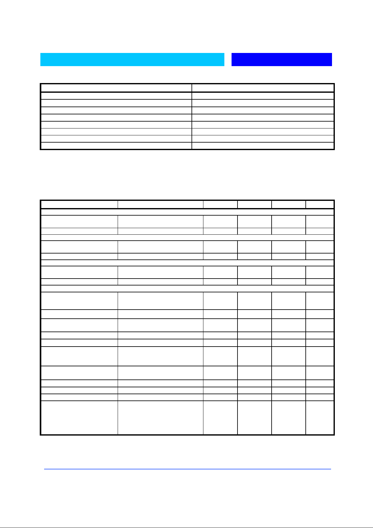
Absolute Maximum Rating
Parameter
Power Dissipation Internally Limited
Lead Temperature ( Soldering 5 seconds )
260 °C
Storage Temperature Range
-65 °C to +150 °C
Operating Junction Temperature
-55 °C to +150 °C
Input Supply Voltage -0.3V to +30V
Feedback Input Voltage -1.5V to +30V
Shutdown Input Voltage -0.3V to +30V
Error Comparator Output -0.3V to +30V
Electrical Characteristics
(VS = 15V, TA = 25°C , unless otherwise specified)
Parameter Conditions MIN TYP MAX UNIT
3.0V Version
Output Voltage
Vin=3.8V I
OUT
=1mA
V IN
≤4.3V, 1mA
≤I
L
≤ 150mA
2.97
2.955
3.00
3.00
3.03
3.045
V
Reverse Output Current B1121-3.0 V
OUT
= 3.0V, VIN = 0V 16 25
µA
3.3V Version
Output Voltage Vin=3.8V I
OUT
=1mA
V IN
≤4.3V, 1mA
≤I
L
≤ 150mA
3.250
3.20
3.30
3.30
3.35
3.366
V
Reverse Output Current B1121-3.3 V
OUT
= 3.3V, VIN = 0V 16 25
µA
5V Version
Output Voltage Vin=3.8V I
OUT
=1mA
V IN
≤4.3V, 1mA
≤I
L
≤ 150mA
4925
4.850
5.00
5.00
5.075
5.150
V
Reverse Output Current B1121-5.0 V
OUT
= 5.0V, VIN = 0V 16 25
µA
Output Voltage
-25 °C ≤ T
j
≤
85 °C
Full Operating Temperature
0.985 [ V
o
]
0.980 [ V
o
]
V
o
1.015 [ Vo ]
1.020 [ V
o
]
V
Output Voltage
100µA ≤ I
L
≤
150mA, T
j
≤ T
jmax
0.976 [Vo ] Vo 1.024 [ Vo ]
V
Output Volt age Temperatu r e
Coefficient
(Note 1) 50 150
ppm / ° C
Line Regulation (Note 3)
V
O
+ 1V ≤ VIN ≤ 30V (Note 4)
0.04 0.4 %
Load Regulation (Note 5)
100µA ≤ I
L
≤
100mA
0.1 0.3 %
Dropout Voltage
I
L
= 100µA
IL = 150mA
50
440
80
550
700
mV
Ground Current
I
L
= 100µA
I
L
= 150mA
75 8 120
14
µ
A
mA
Dropout Ground Current
V
IN
= VO - 0.5V, IL = 100µA
110 170
µ
A
Current Limit V
OUT
= 0 160 200 mA
Thermal Regulation 0.05 0.2 % / W
Output Noise,
10Hz to 100KHz
C
L
= 1µF
C
L
= 200µF
C
L
= 3.3µF
(Bypass = 0.01 µF pins 7 to 1 for
B1121-XX)
430
160
100
µ
Vrms

Bay Linear, Inc
2478 Armstrong Street, Livermore, CA 94550 Tel: (925) 989-7144, Fax: (925) 940-9556 www.baylinear.com
B1121
Note 1:
Output or reference voltage temperature coefficients defined as the worst case voltage change divided by the total temperature range.
Note 2:
Unless otherwise specified all limits guaranteed for T
J
= 25°C, VIN = VO +1V, IL = 100µA and CL = 1µF. Additional conditions for the 8-
pin versions are feedback tied to –XX Voltage tap and output tied to output Sense pin ( V
OUT
= XX V) and V
SHUTDOWN
≤ 0.8V
Note 3:
Regulation is measured at constant junction temperature , using pulse testing with a low duty cycle. Changes in output voltage due to
heating effects are covered under specification for thermal regulation.
Note 4:
Line regulation for B1121-XX is tested at 150°C for I
L
= 1mA. For IL = 100µA and TJ = 125°C, line regulation is guaranteed by design to
0.2%. See typical performance characteristics for line regulation versus temperature and load current.
Note 5:
Dropout voltage is defined as the input to output differential at which the output voltage drops 100mV below its nominal value measured
at 1V differential. At very low values of programmed output voltage, the minimum input supply voltage of 2V (2.3V over temperature) must be
taken into account.
Note 6:
V
REF
≤ V
OUT
≤ (V
IN
–1V), 2.3V ≤ VIN ≤ 30V, 100µA ≤ IL ≤100mA, T
J
≤ T
JMAX
Note 7:
Output or reference voltage temperature coefficient is defined as the worst case voltage change divided by the total temperature range
Note 8:
Comparator thresholds are expressed in terms of a voltage differential at the feedback terminal below the nominal reference voltage
measured at V
O
+ 1V input. To express these thresholds in terms of output voltage change, multiply by the error amplifier gain = V
OUT
/ V
REF
=
(R1 + R2)/R2. For example, at a programmed ou tput voltage of 5V, the error output is guaranteed to go low when t he output drops by 95mV X
5V / 1.235V = 384mV. Thresholds remain constant as a percent of V
OUT
as V
OUT
is varied, with the dropou t warning occu rring at typic ally 5%
below nominal, 7.5% guaranteed.
Note 9:
V
SHUTDOWN
≥ 2V, VIN ≤ 30V, V
OUT
= 0, Feed-back pin tied to –XX Voltage Tap.
 Loading...