BAYLI B1117N-ADJ, B1117N-3.3, B1117N-2.85, B1117N-2.5, B1117N-1.8 Datasheet
...
Bay Linear, Inc
2418 Armstrong Street, Livermore, CA 94550 Tel: (925) 606-5950, Fax: (925) 940-9556 www.baylinear.com
1.0Amp Low Dropout Voltage Regulator
B1117
Adjustable & Fix (0.40Volt Dropout)
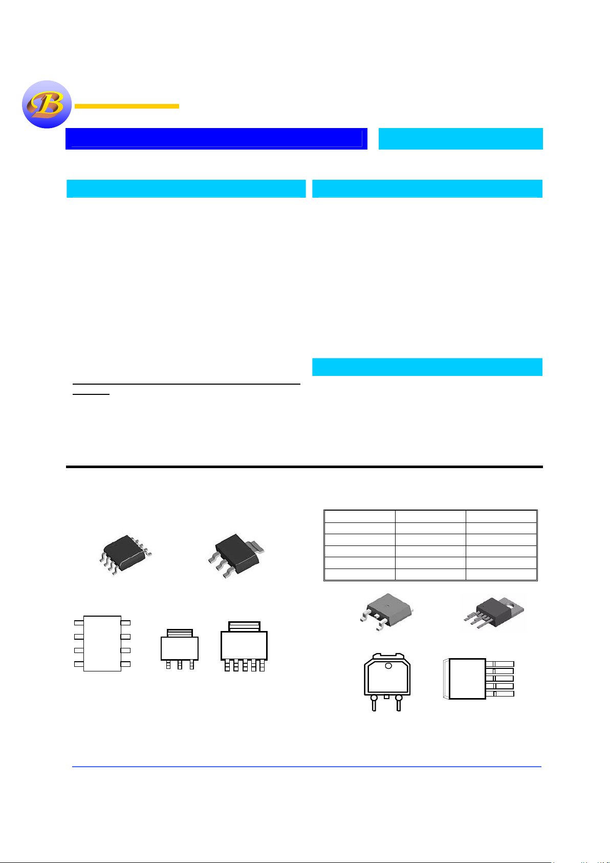
Pin Connection
Ordering Information
Devices Package Temp.
B1117D-X TO-252
0 °C to 125 °C
B1117N-X TO-223
0 °C to 125 °C
B1117T-X TO-220
0 °C to 125 °C
B1117S-X TO-263
0 °C to 125 °C
B1117M-X SO-8
0 °C to 125 °C
2
1
3
4
8
7
6
5
8-Pin Surface Mount
Top View
ADJ
OUT
OUT
N.C.
IN
NC
2
1
3
4
8
7
6
5
8-Pin Surface Mount
Top View
IN
IN
2
1
3
4
8
7
6
5
8-Pin Surface Mount
Top View
ADJ
OUT
OUT
N.C.
IN
NC
2
1
3
4
8
7
6
5
8-Pin Surface Mount
Top View
IN
IN
Description
The Bay Linear B1117 is a three terminal positive NPN
regulator offered as adjustable or fix voltages of 1.5V,1.8V,
2.5V, 2.85V, 3.3V, and 5Volts. The output current has a
capability up to
1.0Amp,. This device has been optimized for
low voltage where transient response and minimum input
voltage are critical. The 2.85V version is designed specifically
to be used in active terminators for SCSI bus.
Current limit is trimmed to ensure specified output current and
controlled short-circuit current. On-Chip thermal limiting
provides protection against any combination of overload and
ambient temperatures that would create excessive junction
temperatures.
The B1117 is offered in a 3-pin SOT-223, and TO-252
(DPAK) packages compatible with other 3 terminal regulators.
5-pin version in TO-263 with lower dropout of 0.4 volt is
available.
Features
• Adjustable Output Down to 1.2V
• Output Current of 1.0Amp
• Low Dropout 1.0V for B1117
• Dropout of 0.40 V in for B1117A
• Adjustable & Fix 1.5V, 1.8V, 2.5V, 2.85V,
3.0V, 3.3V, 5.0V
• 0.05% Load Regulation
• Current & Thermal Limiting
• Lower Cost SOT-89 Package
• Available in SOT-223, and TO-252,
TO-263 & SO-8
• Similar to industry Standard LT1117
Applications
• Active SCSI terminators
• High efficiency Linear Regulator
• Post regulators fro Switching Supplies
• Battery Charger
• 5V to 3.3V linear Regulators
• Motherboard Clock Supplies
Front
TO-252
ADJ/GN
V
IN
V
OUT
1
2 3
IN
OUT Adj/GND
Tab V
OUT
Front View
SOT - 223
IN
OUT Adj/GND
Tab V
OUT
Front View
SOT - 223
V
POWER
OUTPUT
1
2
3
4
5
V
CONTROL
ADJ/GND.
SENSE
TO-263-5 Package
V
POWERVPOWER
OUTPUT
1
2
3
4
5
V
CONTROLVCONTROL
ADJ/GND.
SENSE
TO-263-5 Package
Bay Linear
Inspire the Linear Power
Tab V
OUT
SOT-223
Tab V
OUT
Front View
SOT-223 -5
4
1
5
23
#1 Sense
#2 Adj/GND
#3 OUT
#4 Control
#5 V
IN
Tab V
OUT
SOT-223
Tab V
OUT
Front View
SOT-223 -5
4
1
5
23
#1 Sense
#2 Adj/GND
#3 OUT
#4 Control
#5 V
IN

Bay Linear, Inc
2418 Armstrong Street, Livermore, CA 94550 Tel: (925) 606-5950, Fax: (925) 940-9556 www.baylinear.com
B1117
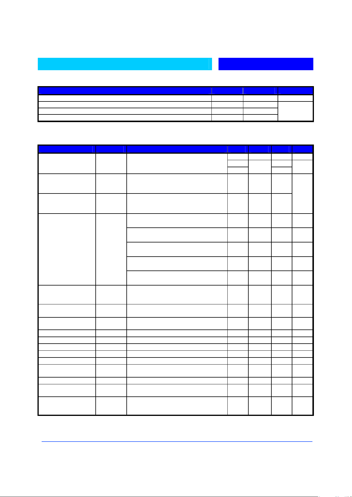
Absolute Maximum Rating
Parameter Min Max Unit
Maximum Input Voltage 7.0 V
Operating Junction Temperature Range 0 125
Storage Temperature Range -65 150
Lead Temperature (Soldering 10 Sec.) 300
°C
Electrical Characteristics
(VIN = 7V; TJ=25°C IO = 10mA to 1.0Amp, unless otherwise specified)
Parameter Symbol Conditions MIN TYP MAX UNIT
1.238 1.250 1.262 V
1.225 1.275
Reference Voltage VO 1117-adj, I
OUT
=10mA, VIN-V
OUT
=2V, TJ=25°C
1.5V≤(V
IN-VOUT
) ≤5.75V
10mA≤I
OUT≤IFULL LOAD
-2%
1.250
+2%
V
Line Regulation (1) REG
(line)
(V
OUT
+1.5)≤VIN≤7V, I
OUT
=10mA
0.005 0.2
Load Regulation (1) REG
(LOAD)
(Vin-V
out
)=2V
10mA≤I
OUT≤IFULL LOAD
T= 25 °C
0.05 0.5
%
1117-1.8 I
OUT
=10mA, VIN=3.8V, TJ=25°C
0≤I
OUT
≤1.0Amp, 3.2V≤VIN≤7V
1.782
1.746
1.80
1.80
1.818
1.854
V
1117-2.5 I
OUT
=10mA, VIN=4.5V, TJ=25°C
0≤I
OUT
≤1.0Amp, 4.0V≤VIN≤7V
2.475
2.450
2.50
2.50
2.525
2.550
V
1117-2.85 I
OUT
=10mA, VIN=4.85V, TJ=25°C
0≤I
OUT
≤1.0Amp, 4.35V≤VIN≤7V
2.820
2.790
2.85
2.85
2.880
2.910
V
1117-3.3 I
OUT
=10mA, VIN=5.0V, TJ=25°C
0≤I
OUT
≤1.0Amp, 4.8V≤VIN≤7V
3.267
3.235
3.30
3.30
3.333
3.365
V
Output Voltage VO
1117-5.0 I
OUT
=10mA, VIN=6.0V, TJ=25°C
0≤I
OUT
≤1.0Amp, 6.5V≤VIN≤7V
4.950
4.900
5.00
5.00
5.050
5.100
V
Dropout Voltage V
D
Control Input
V
POWER=VOUT
+0.8, I
LOAD
=10mA
V
POWER=VOUT
+0.8, I
LOAD
=1.0Amp,
0.80
0.80
1.00
1.10
V
Dropout Voltage VD Power Input
V
CONTROL=VOUT
-+2.5V, I
LOAD
=1.0Amp,
0.35 0.40 V
Current Limit I
S
(Vin-V
out
)=2V
1.0 1.1 A
Minimum Load Current I
MIN LOAD
1.5V≤(VIN-V
OUT
) ≤5.75V
10 mA
Temperature Regulation T
A
T= 25 °C, 30ms pulse
0.004 0.02 %/W
Long Term Stability -
T= 25 °C, 1000Hrs
0.03 1.0 %
Temperature Stability T
S
0.5 %
Adjust pin Current -
T= 25 °C
35 120
µA
Ripple Rejection R
A
F=120Hz, C
ADJ
=22µF, C
OUT
=22µF Tantalum
I
OUT=IFULL LOAD
, (Vin-V
out
)=3V (Note 5)
60 75 dB
Thermal Shutdown 155
°C
Thermal Shutdown
Hysterics
10
°C
Thermal Resistance
Junction to case
-
SOT-223
DD Package
15
3.0
15
3.0
°C/W
Note: Output Switch tests are performed under pulsed conditions to minimize power dissipation

Bay Linear, Inc
2418 Armstrong Street, Livermore, CA 94550 Tel: (925) 606-5950, Fax: (925) 940-9556 www.baylinear.com
B1117
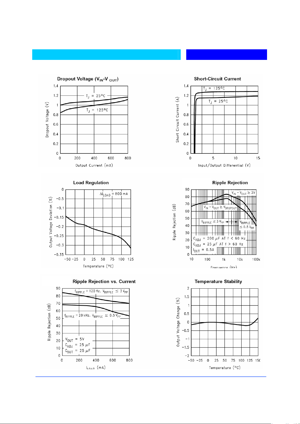
TYPICAL CHRACTRISTICS
B1117-2.85
B1117-ADJ
 Loading...