BAYLI B1085T-ADJ, B1085S-ADJ, B1085D-ADJ Datasheet

Bay Linear, Inc
2478 Armstrong Street, Livermore, CA 94550 Tel: (925) 989-7144, Fax: (925) 940-9556 www.baylinear.com
3.0A Low Dropout Voltage Regulator
B1085
Adjustable
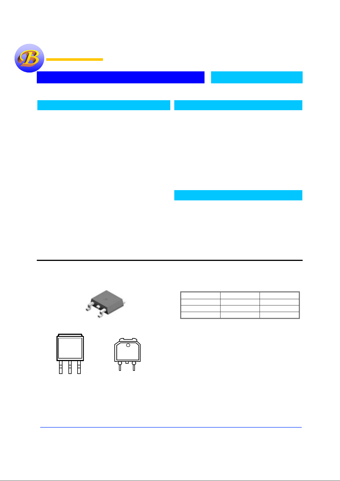
Pin Connection
Ordering Information
Devices Package Temp.
B1085T TO-220
0 °C to 70 °C
B1085S TO-263
0 °C to 70 °C
B1085D TO-252
0 °C to 70 °C
Description
The Bay Linear B1085 is Monolithic low power 3.0A
Adjustable and fixed NPN voltage regulator that are easy to
use with minimum external components. All internal circuitry
is designed to operate down to 1V input to output differential
and the dropout vo ltage is fully sp ecified as a functi on of load
current. Dropout is guaranteed at a maximum of 1.5V at a
maximum output current. Current limit is trimmed, minimizing
the stress on both the regulator and power source circuitry
under overload conditions. It is suitable for applications
requiring a well-regulated positive output voltage with low
input-output differential voltag e .
The B1085 Outstanding features include full power usage up
to 3.0Amp of load current internal current limiting and thermal
shutdown. A 10 µF output capacito r is required on these new
devices; how ever, this is usually included in most regulator
design.
The B1085 is offered in a 3-pin TO-220, TO-263 & TO-252
packages compatible with other 3 terminal regulators. For 5A
Low dropout Regulator refer to the BL1084 data sheet.
Features
• Adjustable Output Down to 1.2V
• Output Current of 3.0A
• Low Dropout Voltage 1.0V Typ.
• 0.015% Line Regulation
• 0.01% Load Regulation
• Current & Thermal Limiting
• Standard 3-Terminal Low Cost TO-220,
D
2
, D Packages
•
Similar to industry Standard LT1085
Applications
• Constant Current Regulators
• SMPS Post Regulator
• High Efficiency Linear Regulator
• High Efficiency Linear Power Supplies
• Battery Charger
• Adjustable Power Supplies
Bay Linear
Bay LinearBay Linear
Bay Linear
Linear Excellenc e
Front View
TO-252 (D)
ADJ/
GND
V
IN
V
OU
T
1
23
Top View
TO-263-3 (S)
1
Bay Linear
2
3
Top View
TO-263-3 (S)
1
Bay Linear
2
3
Top View
TO-263-3 (S)
1
Bay Linear
2
3
Top View
TO-263-3 (S)
1
Bay Linear
2
3

Bay Linear, Inc
2478 Armstrong Street, Livermore, CA 94550 Tel: (925) 989-7144, Fax: (925) 940-9556 www.baylinear.com
B1085
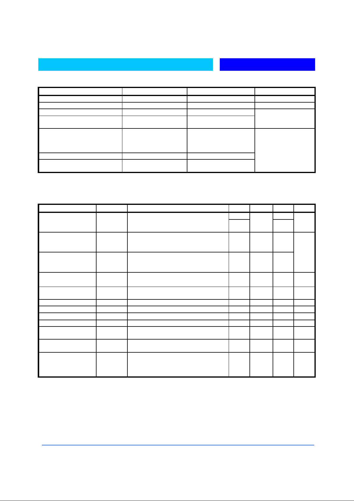
Absolute Maximum Rating
Parameter Symbol Value Unit
Maximum Input Voltage V
IN
30 V
Power Dissipation P
O
Internally Limited W
Thermal Resistance Junction to Case
θ
JC
3
Thermal Resistance Junction to
Ambient
θ
JA
50
°
C/W
Operating Junction
Temperature Range
Control Section
Power Transistor
T
J
0 to 125
0 to 150
Storage Temperature Range T
STG
-65 to 150
Lead Temperature (Soldering 10
Sec.)
T
LEAD
300
°
C
Electrical Characteristics
(VIN = 4.75V to 5.25V; IO = 10mA to 3.0Amp, unless otherwise specified)
Parameter Symbol Conditions MIN TYP MAX UNIT
1.238 1.262 Reference Voltage V
O
IO = 10mA,T= 25 °C, Vin-V
out
=3V
10mA≤I
OUT
≤
I
FULL LOAD
1.5V≤(Vin-V
out
) ≤25V (Note3)
1.225
1.250
1.270
V
Line Regulation (1) REG
(line)
I
LOAD
= 10mA, 1.5V≤(VIN – V
OUT
) ≤15V
T= 25 °C
15V≤(V
in-Vout
) ≤30V
0.015
0.035
0.05
0.20
0.20
0.50
Load Regulation (1) REG
(LOAD) (Vin-Vout
)=3V
10mA≤I
OUT
≤
I
FULL LOAD
T= 25 °C
0.1
0.2
0.30
0.40
%
Dropout Voltage V
D
T= 25 °C
Over Temperature
1.3 1.5 V
Current Limit I
S
(Vin-V
out
)=5V
(V
in-Vout
)=25V
3.2
0.2
4
0.5
A
Mini mum Load Current I
MIN LOAD
(Vin-V
out
)= 25V 10 10 mA
Temperature Regulation T
A
T= 25 °C, 30ms pulse
0.004 0.02 %/W
Long Term Stability -
T= 25 °C, 1000Hrs
0.3 1
Temperature Stability T
S
0.5 %
Adjust pin Current -
T= 25 °C
Over Temp.
55
120
µ
A
Ripple Rejection R
A
F=120Hz, C
ADJ
=25µF, C
OUT
=25µF Tantalum
I
OUT=IFULL LOAD
, (Vin-V
out
)=3V (Note 5)
60 75 dB
Thermal Resistance - TO-220 Junction to Tab
Junction to Ambient
DD Package Junction to Tab
Junction to Ambient
3.0
60
3.0
60
3.0
60
3.0
60
°
C/W
Note:
Output Switch tests are performed under pulsed conditions to minimize power dissipation
 Loading...