


Rhein Tech Laboratories, Inc.
Client:
Banner Engineering Corporation
360 Herndon Parkway
Model:
RM912HP
Suite 1400
Standards:
FCC 15.247/IC RSS-210
Herndon, VA 20170
http://www.rheintech.com
ID’s:
UE3RM912HP/7044A-RM912HP
Report #:
2009324
Appendix L: Manual
Please refer to the following pages for the FHSS and DTS manuals.

Banner RM912HP Transceiver
1 Watt, 900 MHz FHSS Module
User Manual
Overview
The Banner RM912HP device is a frequency hopping spread spectrum transceiver
operating in the 902 – 928 MHz band. It is an implementation of a particular ISM band
transceiver IC that includes an external LNA in the receive path and external 1 W power
amplifier in the transmit path, as well as all necessary RF switches and matching
components. Users need only supply power and ground, control signals, and a controlled
impedance path to one of our FCC approved antennas to fully implement the device
transceiver.
Typical users of this module are projects that are conceived and built by Banner
engineering, usually for low power wireless sensor network telemetry. Projects will
fundamentally be time division multiple access (TDMA) architecture with frequency
hopping spread spectrum (FHSS) employed for distributing RF energy evenly across the
ISM band.
Users will have to comply with the hopping schedule, number of channels, dwell
times, and other parameters that are covered in FCC part 15, and bounded by the limits
set up in the test report. All questions regarding these limits should be directed to the
factory.
This certification only covers operation of the transceiver in particular modes of
modulation scheme and data rate. Be aware that there are modes of operation on the
transceiver IC that are not covered by this certification and must be avoided by the user.
This document will discuss fixed and configurable parameters and their relation to
meeting the FCC specifications. Such parameters include the frequency plan, the time
sharing architecture, power control, and approved antennas.
Frequency Plan
The radio is licensed to transmitting or receiving on any of 50 equally spaced,
non-overlapping channels available in the 902-928 MHz band. (903, 903.5, 904, 927.5
MHz) The hop table should be chosen from this bin of 50 frequencies in a pseudorandom fashion without replacement so as to avoid repeats before the entire table is
traversed.
TDMA Plan
The radio is intended for operation in deterministic and ad-hoc networks. The
communications channel is shared in these networks using a time domain multiple access
protocol. The underlying structure to this protocol is a frame made up of N time slots,
each of length T
transmitting (T
time on any given transmit channel below 64 ms in any given 100 ms window.
. During each time slot, a given radio could spend part of its time
slot
), receiving, or idle to conserve energy. Users must keep the total dwell
on
Page 1 of 5

Power Control
Users that wish to utilize the entire 1 W transmit capability of this radio must also
ensure that they are using all 50 frequencies. Users that do not wish to use all 50
frequencies must then compensate by keeping the transmit power level below 250 mW,
and still must use at least 25 frequencies. Contact the factory for details on adjusting RF
power levels.
Operation
Operational details for the radio appear in the PowerPoint document
“RM912HP_01_operational_description”. This is the document to refer to for
connection diagrams, pad layouts, and other implementation details. The other primary
reference is the data sheet for the transceiver IC. Please contact Banner Engineering for
copies of that reference.
Antenna Choices
The following classes of antennas (Table 1) were tested and approved for use with the
RM912HP.
Approved antennas
Antenna style Gain
High gain helical loaded omnidirectional monopole
High gain omnidirectional dipole
High gain Yagi directional
Antennas of like design with less gain than the type tested may also be used. The device
must always be professionally installed using unique connectors.
<= 5 dBi
<= 8 dBi
<= 6 dBi)
Table 1
Page 2 of 5
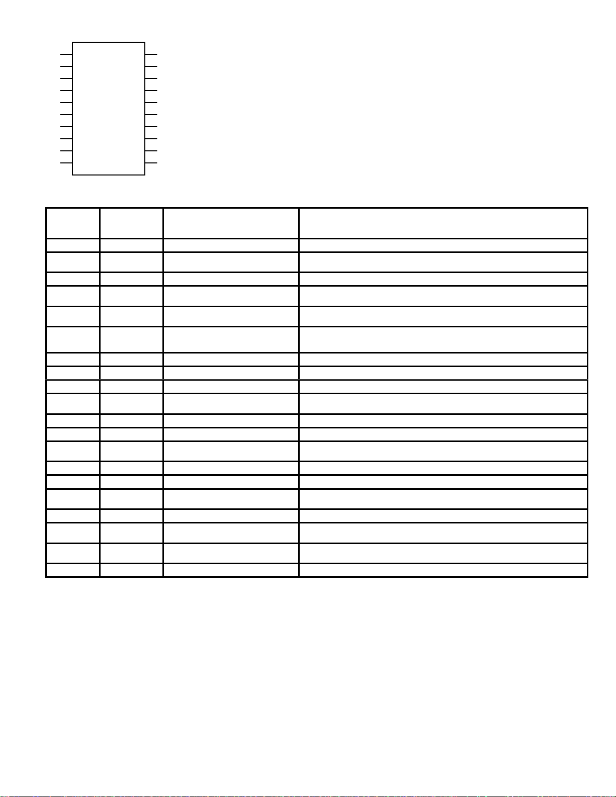
1
2
3
RM912HP Schematic
4
5
6
7
8
9
10
20
19
18
17
16
15
14
13
12
11
Connection Diagram and
Instructions.
Pin # Pin
Pin Function Connection Instructions
Name
1 G1 RF Ground Via directly to ground.
2 RF RF Signal Route a 50 ohm trace to the antenna.
3 G3 RF Ground Via directly to ground.
4 SW1 Switch 1 ctrl – active low Tx Logic low for Tx, high for Rx
5 SW2 Switch 2 ctrl – active low Rx Logic high for Tx, low for Rx
6 V Vdd, general purpose
Supply 2.7 V, +/- 10%
supply
7 G2 Ground Signal ground
8 TP2 Power Amp Enable Power amp enable.
9 Reset Transceiver ~RST See Transceiver datasheet.
10 Select Transceiver ~SEL (for SPI) See Transceiver datasheet.
11 MISO Transceiver Data Out SPI data out of Transceiver
12 MOSI Transceiver Data In SPI data in to Transceiver
13 SCLK Transceiver SPI Clock SPI Clock, see Transceiver datasheet for usage guidelines.
14 DIG2 Transceiver DIG2 See Transceiver datasheet.
15 G4 Ground Signal ground
16 V2 Power Amp VCC Supply 1.5 – 2.7 V during transmit
17 LNA Bias LNA Enable Low = ON, HI-Z = OFF
18 LNA Gain LNA Gain Control High for high linearity, low for high gain.
19 SLP_TR Atmel SLP_TR See Transceiver datasheet; pulse high to initiate Tx
20 IRQ Atmel IRQ Various interrupt sources
Page 3 of 5

RF Exposure Statement:
This equipment has a power density well below that allowed at 23 cm; therefore, this
equipment shall be installed and operated with an antenna with gain not more than
8 dBi and installed with a minimum of 23 cm of separation distance between the
antenna and all persons during normal operation.
FCC Regulations Statement
FCC ID: UE3RM912HP This device complies with Part 15 of the FCC Rules.
Operation is subject to the following two conditions: (1) this device may not cause
harmful interference, and (2) this device must accept any interference received, including
interference that may cause undesired operation.
FCC Notices
IMPORTANT: The radio modules have been certified by the FCC for use with other
products without any further certification (as per FCC section 2.1091). Changes or
modifications not expressly approved by the manufacturer could void the user’s authority
to operate the equipment.
IMPORTANT: The radio modules have been certified for fixed base station and mobile
applications. If modules will be used for portable applications, the device must undergo
SAR testing.
IMPORTANT: If integrated into another product, the FCC ID label must be visible
through a window on the final device or it must be visible when an access panel, door, or
cover is easily removed. If not, a second label must be placed on the outside of the final
device that contains the following text: Contains FCC ID: UE3RM912HP.
Banner RM912HP Radio Module Specification
Frequency Band 902- 928 MHz
Modulation method BPSK, O-QPSK
Spectrum widening Frequency Hopping Spread Spectrum
(FHSS), or DTS for 1000 kb/s rates
Number of channels Typically 50 or less
Individual channel bandwidth Variable depending on data rate
Channel separation Variable depending on data rate
Radiated power +30 dBm (1 W) max for FHSS modes,
+26 dBm for DTS modes
Power supply 3.0 Vdc
Supply current 1000 mA @ 3V
Digital Interface SPI
Interface data rate 4000 kbits/sec
Sensitivity -104 dBm
Page 4 of 5

RF Data rate Selectable, see datasheet
Mechanical dimensions 20 x 28 mm
Page 5 of 5

Banner RM912HP Transceiver
1 Watt, 900 MHz DTS
User Manual
Overview
The Banner RM912HP device is a direct sequence spread spectrum transceiver
(DSSS) operating in the 902 – 928 MHz band. It is an implementation of a particular
ISM band transceiver IC that includes an external LNA in the receive path and external
power amplifier in the transmit path, as well as all necessary RF switches and matching
components. Users need only supply power and ground, control signals, and a controlled
impedance path to one of our FCC approved antennas to fully implement the device
transceiver.
Typical users of this module are projects that are conceived and built by Banner
engineering, usually for low power wireless sensor network telemetry. Projects will
fundamentally be time division multiple access (TDMA) architecture with DSSS
employed for distributing RF energy evenly across the ISM band.
Users will have to comply with the modulation schemes, number of channels,
dwell times, and other parameters that are covered in FCC part 15, and bounded by the
limits set up in the test report. All questions regarding these limits should be directed to
the factory.
This certification only covers operation of the transceiver in particular modes of
modulation scheme and data rate. In particular, the device is licensed for to operate
within the parameters of the IEEE 802.15.4 standard, which deals with 40 kb/s or 250
kb/sec data. It is also licensed for a proprietary 1000 kb/s mode that has nearly the same
spectrum as an 802.15.4 mode. Be aware that there are modes of operation on the
transceiver IC that are not covered by this certification and must be avoided by the user.
This document will discuss fixed and configurable parameters and their relation to
meeting the FCC specifications. Such parameters include the frequency plan, the time
sharing architecture, power control, and approved antennas.
Frequency Plan
The radio is licensed to transmitting or receiving on any of 10 equally spaced,
non-overlapping channels available in the 902-928 MHz band (906, 908 …924 MHz)
when it is operating in the standard 802.15.4 compliant modes. In the proprietary 1000
kb/s mode, there are 17 equally spaced frequencies available (903, 904.5 …927 MHz)
Because it is operating under DTS rules, changing frequencies isn’t specifically required,
but it is still a good practice.
TDMA Plan
The radio is intended for operation in deterministic and ad-hoc networks. The
communications channel is shared in these networks using a time domain multiple access
protocol. The underlying structure to this protocol is a frame made up of N time slots,
Page 1 of 5

each of length T
. During each time slot, a given radio could spend part of its time
slot
transmitting (Ton), receiving, or idle to conserve energy. To be in compliance with the
rules for dwell time as tested, the radio transmitter must be on less than 50 % of the time.
Power Control
Users must ensure that they are maintain a conducted output power of 26 dBm or
less. Contact the factory for details on adjusting RF power levels.
Operation
Operational details for the radio appear in the PowerPoint document
“RM912HP_06_user_manual”. Refer to that document for connection diagrams, pad
layouts, and other implementation details. The other primary reference is the data sheet
for the transceiver IC. Please contact Banner Engineering for copies of that reference.
Antenna Choices
The following classes of antennas (Table 1) were tested and approved for use with
the RM912HP.
Approved antennas
Antenna style Gain
High gain helical loaded omnidirectional monopole
High gain omnidirectional dipole
High gain Yagi directional
Antennas of like design with less gain than the type tested may also be used. The device
is always professionally installed and uses unique connectors.
<= 5 dBi
<= 8 dBi
<= 6 dBi)
Table 1
Page 2 of 5

RM912HP Schematic
Connection Diagram and
Instructions.
10
1
2
3
4
5
6
7
8
9
20
19
18
17
16
15
14
13
12
11
Pin # Pin
Pin Function Connection Instructions
Name
1 G1 RF Ground Via directly to ground.
2 RF RF Signal Route a 50 ohm trace to the antenna.
3 G3 RF Ground Via directly to ground.
4 SW1 Switch 1 ctrl – active low Tx Logic low for Tx, high for Rx
5 SW2 Switch 2 ctrl – active low Rx Logic high for Tx, low for Rx
6 V Vdd, general purpose
supply
7 G2 Ground Signal ground
8 TP2 Power Amp Enable Power amp enable.
9 Reset Transceiver ~RST See Transceiver datasheet.
10 Select Transceiver ~SEL (for SPI) See Transceiver datasheet.
11 MISO Transceiver Data Out SPI data out of Transceiver
12 MOSI Transceiver Data In SPI data in to Transceiver
13 SCLK Transceiver SPI Clock SPI Clock, see Transceiver datasheet for usage guidelines.
14 DIG2 Transceiver DIG2 See Transceiver datasheet.
15 G4 Ground Signal ground
16 V2 Power Amp VCC Supply 1.5 – 2.7 V during transmit
17 LNA Bias LNA Enable Low = ON, HI-Z = OFF
18 LNA Gain LNA Gain Control High for high linearity, low for high gain.
19 SLP_TR Atmel SLP_TR See Transceiver datasheet; pulse high to initiate Tx
20 IRQ Atmel IRQ Various interrupt sources
Supply 2.7 V, +/- 10%
Page 3 of 5

RF Exposure Statement:
This equipment has a power density well below that allowed at 20 cm; therefore, this
equipment shall be installed and operated with an antenna with gain not more than
8 dBi and installed with a minimum of 20 cm of separation distance between the
antenna and all persons during normal operation.
FCC Regulations Statement
FCC ID: UE3RM912HP This device complies with Part 15 of the FCC Rules.
Operation is subject to the following two conditions: (1) this device may not cause
harmful interference, and (2) this device must accept any interference received, including
interference that may cause undesired operation.
FCC Notices
IMPORTANT: The radio modules have been certified by the FCC for use with other
products without any further certification (as per FCC section 2.1091). Changes or
modifications not expressly approved by the manufacturer could void the user’s authority
to operate the equipment.
IMPORTANT: The radio modules have been certified for fixed base station and mobile
applications. If modules will be used for portable applications, the device must undergo
SAR testing.
IMPORTANT: If integrated into another product, the FCC ID label must be visible
through a window on the final device or it must be visible when an access panel, door, or
cover is easily removed. If not, a second label must be placed on the outside of the final
device that contains the following text: Contains FCC ID: UE3RM912HP.
Banner RM912HP Radio Module Specification
Frequency Band 902- 928 MHz
Modulation method BPSK, O-QPSK
Spectrum widening Frequency Hopping Spread Spectrum
(FHSS), or DTS for 1000 kb/s rates
Number of channels Typically 50 or less
Individual channel bandwidth Variable depending on data rate
Channel separation Variable depending on data rate
Radiated power +30 dBm (1 W) max for FHSS modes,
+26 dBm for DTS modes
Power supply 3.0 Vdc
Supply current 1000 mA @ 3V
Digital Interface SPI
Interface data rate 4000 kbits/sec
Sensitivity -104 dBm
Page 4 of 5

RF Data rate Selectable, see datasheet
Mechanical dimensions 20 x 28 mm
Page 5 of 5
 Loading...