

Page 1

BandLuxeTM
M250 Series HSUPA Module
User Manual
Page 2

Page 3

Class: User Manual
Doc. No.: M250-D-001
Doc. Version: 1.0
Publish Date: 2008-Dec-05
THE SPECIFICATIONS AND INFORMATION REGARDING THE PRODUCTS IN THIS MANUAL ARE SUBJECT
TO CHANGE WITHOUT NOTICE. ALL STATEMENTS, INFORMATION, AND RECOMMENDATIONS IN THIS
MANUAL ARE BELIEVED TO BE ACCURATE BUT ARE PRESENTED WITHOUT WARRANTY OF ANY KIND,
EXPRESS OR IMPLIED. USERS MUST TAKE FULL RESPONSIBILITY FOR THEIR APPLICATION OF ANY
PRODUCTS.
THE SOFTWARE LICENSE AND LIMITED WARRANTY FOR THE ACCOMPANYING PRODUCT ARE SET
FORTH IN THE INFORMATION PACKET THAT SHIPPED WITH THE PRODUCT AND ARE INCORPORATED
HEREIN BY THIS REFERENCE.
NOTWITHSTANDING ANY OTHER WARRANTY HEREIN, ALL DOCUMENT FILES AND SOFTWARE OF
THESE SUPPLIERS ARE PROVIDED “AS IS” WITH ALL FAUL TS. PRODUCT AND THE ABOVE-NAMED
SUPPLIERS DISCLAIM ALL WARRANTIES, EXPRESSED OR IMPLIED, INCLUDING, WITHOUT LIMITATION,
THOSE OF MERCHANTABILITY, FITNESS FOR A PARTICULAR PURPOSE AND NONINFRINGEMENT OR
ARISING FROM A COURSE OF DEALING, USAGE, OR TRADE PRACTICE.
IN NO EVENT SHALL PRODUCT OR ITS SUPPLIERS BE LIABLE FOR ANY INDIRECT, SPECIAL,
CONSEQUENTIAL, OR INCIDENTAL DAMAGES, INCLUDING, WITHOUT LIMITATION, LOST PROFITS OR
LOSS OR DAMAGE TO DATA ARISING OUT OF THE USE OR INABILITY TO USE THIS MANUAL, EVEN IF
PRODUCT OR ITS SUPPLIERS HAVE BEEN ADVISED OF THE POSSIBILITY OF SUCH DAMAGES.
BandRich M250
Datasheet
Document Number: M250-D-001
BandRich Inc.
7F., No. 188, Baociao Rd., Sindian City
T AIPEI, TAIWAN, R.O.C.
http://www.bandrich.com
COPYRIGHT ©2007-2008 BandRich All rights reserved.
Page 4

Table of Contents
Section 1 Introduction..........................................................................1-2
Section 2 Device Driver Interface........................................................2-2
Section 3 AT Command Set Reference...............................................3-2
Section 4 Packing Information.............................................................3-2
Section 5
FCC Statement......................................................................5-1
Page 5
Section 1 Introduction
1.1 General Description
The M250 module series is PCI Express Mini Card providing WWAN (HSUPA, HSDPA, WCDMA,
EGPRS, and GPS) connectivity to laptops or any other device equipped with a PCI Express Mini Card
slot.
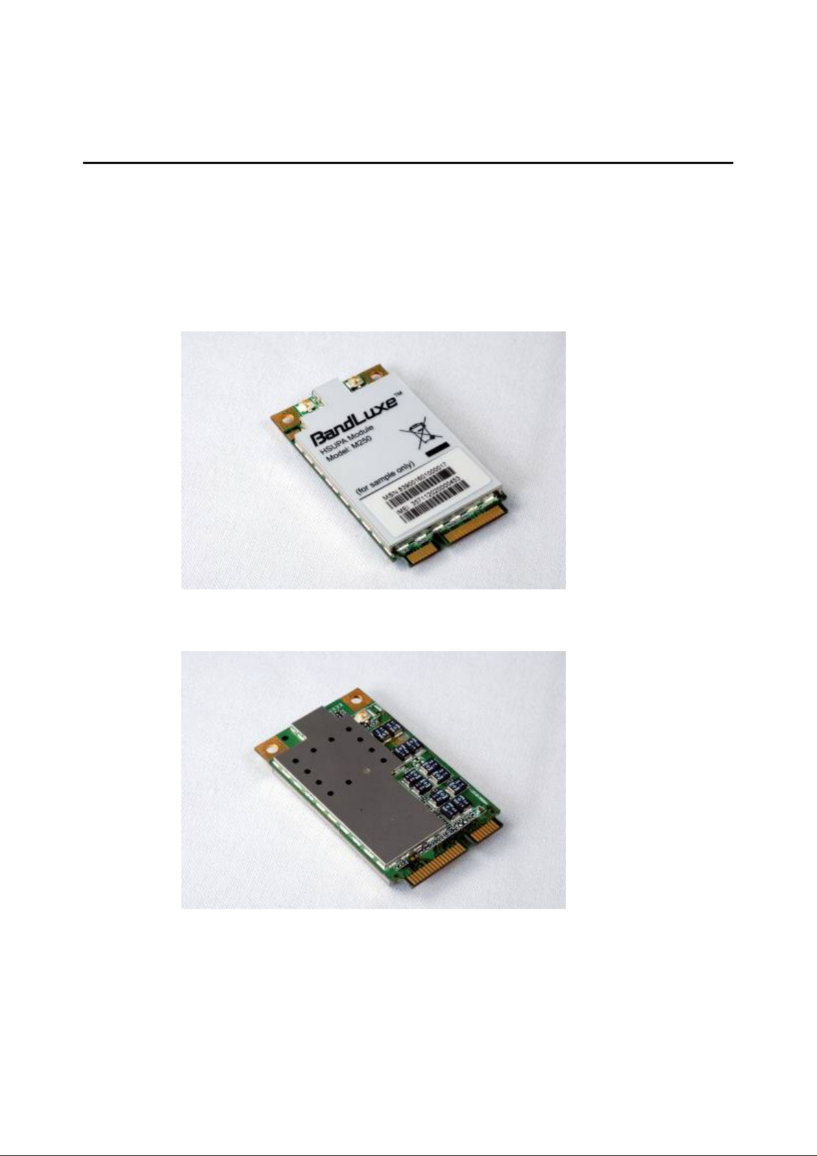
Figure 1-1 Top View
Figure 1-2 Bottom View
Page 6

1.2 Features
1.2.1 WCDMA
y FDD 850/1900/2100 MHz
y Power Class 3 (+24dBm)
y WCDMA 384/384 kbps downlink/uplink modem operation
y HSUPA 2Mbps uplink modem operation (SW upgradable to 5.7Mbps)
y HSDPA 7.2Mbps downlink modem operation
y Supports UL and DL Compressed Modes
y Supports Circuit and Packet-Switched Data
y M250V supports 3G voice call via PCM interface
1.2.2 E-GPRS
y 850/900/1800/1900 MHz
y GSM Power Class 4 (2W) for 850/900 bands
y GSM Power Class 1 (1W) for 1800/1900 bands
y EDGE class E2 (+27 dBm in 850/900 bands, +26 dBm in 1800/1900 bands)
y GPRS/EGPRS Multislot Class 12 (4 slots Rx, 4 slots Tx, 5 slots active max)
y GPRS/EGPRS Class B Type 1 MT
y GPRS CS1-CS4; EGPRS MCS1-MCS9
y Circuit Switched Data: 14.4 and 9.6 kbps
y M250V supports GSM voice call via PCM interface
1.2.3 GPS
y High-sensitivity GPS that integrated in Qualcomm gpsOne solution.
y High availability that is enabled by using both satellite and network information.
y The GPS RF path is shared with the UMTS Receive Diversity RF path. When the GPS
functionality is enabled, the UMTS Receive Diversity will be disabled.
1.2.4 Baseband Functionality
The M250 module interfaces with host device through PCI Express Mini Card interface. The
interface equips with USB2.0 interface, USIM interface, LED control signal, Wake# signal to request
host device return from sleep/suspended state, and W_Disable# signal to disable radio operation.
There are several GPIO pins (2.6V compatible) reserved for customized applications, please contact
BandRich for discussion. Besides the above mentioned interfaces, M250V also provides PCM
interfaces reserved for voice applications. The M250-LC features low power consumption but
requires higher input voltage than PCI standard.
1.2.5 Software Functionality
M250 module series is supplied with device driver of Microsoft Windows Vista 32/64, Windows XP
SP2 above, Windows 2000 SP4 above, Mac OSX 10.4 above, and Linux Fedora 8, Unbuntu 7, Open
SuSE 10.
Page 7

1.3 M250 PCI-Express Mini Card Interface
1.3.1 Pin Description
Table 1-1 M250 Module Series Connector Pin-out
Pin No. Name Pin No. Name
1 WAKE#/GPIO1 (optional) 2 Vaux
3 PCM_DOUT (M250V only) 4 GND
5 PCM_DIN (M250V only) 6 N.C./GPIO2 (optional)
7 N.C. 8 UIM_PWR
9 GND 10 UIM_DATA
11 PCM_SYNC (M250V only) 12 UIM_CLK
13 PCM_CLK (M250V only) 14 UIM_RESET
15 GND 16 N.C.
17 N.C. 18 GND
19 N.C. 20 W_DISABLE#
21 GND 22 HW_RST#
23 N.C./GPIO3 (optional) 24 Vaux
25 N.C. 26 GND
27 GND 28 N.C.
29 GND 30 N.C.
31 N.C. 32 N.C.
33 N.C. 34 GND
35 GND 36 USB_D37 GND 38 USB_D+
39 Vaux 40 GND
41 Vaux 42 LED_WWAN# *
43 GND 44 N.C.
45 N.C. 46 N. C.
47 N.C. 48 N.C.
49 N.C. 50 GND
51 N.C. 52 Vaux
For more information, please refer to PCI-SIG, PCI Express Mini Card Electromechanical
Specification 1.2. http://www.pcisig.com/home
Page 8

Figure 1-3 Pin-out information of M250 series (Top View)
1.4 Network LED indicate device
The Network LED indicated device is ground-referenced current sink. The host drives the device to
provide a current path and an appropriate voltage for LED at PIN 42 of M250 module. Figure 2-2
shows the block diagram of the current drivers. Table 2-3 describes the LED output characteristics in
different states.
Figure 1-4 LED Current Driver Example
VDD
PIN42
Table 1-2 LED Output
M250 Module
Current Control
LED State Module Status Description LED Characteristics
OFF Module is not powered. LED is OFF.
ON
Slow blink
Module is powered and camped on
network, but not transmitting or receiving.
Module is powered and searching for
network (not yet registered on network).
LED is continuously ON.
LED is flashing at a steady slow
speed.
250ms±5% ON period and
750ms±5% OFF period
Page 9

LED State Module Status Description LED Characteristics
LED is flashing intermittently
Intermittent
blink
Module is transmitting or receiving
during data transfer activity.
50ms±5% ON period and
250ms±5% OFF period
Page 10

USB Interface
M250, M250V and M250-LC module are compliant with USB2.0 in all three modes (Low speed, Full
speed, and high speed). When two devices are connected via a USB interface, one of the devices must
act as a host, and the other device must act as a peripheral. The host is responsible for initiating and
controlling traffic on the bus. For example, the USB specification requires PCs to act as hosts, and
other devices such as M250 to act as devices.
Figure 1-5 USB Interface
1.5 USIM Interface
The universal subscriber identification module (USIM) is a smart card for UMTS/GSM cellular
applications. The USIM provides the required subscription information to allow the mobile equipment
to attach to a GSM or UMTS network. The USIM also provides the subscriber's verification
procedures as well as authentication methods for network authentication during the network
registration procedures. Upon power-up or after a soft-reset, the clock and data lines to the USIM will
be active through the initialization process. Figure 2-3 shows the SIM card pin definition. It’s
recommended to implement hardware USIM detection mechanism or complete avoiding USIM
hot-plug through mechanical design. The reference design for hardware USIM detection is provided
in the “Application Note for BandLuxe Module USIM Detection Recommendation”.
Table 1-3 SIM Card Pin Definition
Pin No. Description
1 Vcc
2 RST
3 CLK
4 GND
5 Vpp
6 I/O
Page 11

y USIM_CLK and USIM_RST signal, include 33pF filter capacitors is required to be placed near
the SIM connector.
y Route all USIM signals carefully – isolate them from sensitive analog and RF signals.
y External ESD diodes are necessary to protect the chip on the module; the ESD diodes should be
placed near the connector.
y Refer to the reference circuits below:
1.6 Figure 1-6 Antenna Guidelines and RF Connection
This section describes general guidelines for the design of multi-band antenna required for the M250
module series.
1.6.1 Antenna specifications
Frequency range
y GSM850 (824-894 MHz)
y EGSM900 (880-960 MHz)
y DCS1800 (1710- 1880 MHz)
y PCS1900 (1850-1990 MHz)
y WCDMA 850/1900/2100 (824-894 / 1850-1990 / 1920-2170 MHz)
y GPS (1575.42MHz±1.023MHz)
Maximum permitt ed pe ak gain: -5.8dBi at 850MHz and -0.31dBi at 1850MHz
Maximum VSWR
y < 2.5:1 with 50 reference impedance
Polarization
y Linear
1.6.2 Antenna connector
The antenna connector type used is a U.FL microwave coaxial connector. It is also can be used for
testing purpose.
Figure 1-7 Antenna Connector Position and Type
Main Antenna
Connector
GPS RF Connector
Diversity Antenna
Connector
Page 12

Section 2 Device Driver Interface
Basically the module will manifest itself as a composite USB device which creates stubs which the
other higher level drivers hook into and provide their respective function. The composite USB device
could be modem, NDIS interface, AT command interface or diagnostics interface. All device drivers
used by OS have been created for Microsoft Windows Vista 32/64, Windows XP SP2 above, Windows
2000 SP4 above, Mac OSX 10.4 above, and Linux Fedora 8, Unbuntu 7, Open SuSE 10.
Either the modem or the NDIS interface can be used to transfer data; and AT command interface or
diagnostic interface could be used to send/receive information of the module via the Connection
Manager (CM) application. For more information about supporting AT commands please refer to
section 3.
Page 13

Section 3 AT Command Set Reference
Table B-1 lists the standard AT command that are implemented in BandLuxe M250 module series.
For detail command usage and possible response, please check 3GPP TS 27.007, AT command set for
User Equipment (UE).
Table B-1 A bbrev iations and Acronyms Table
BandLuxe HSPA Modem AT Command Interface API
Serial Port Name: BandLuxe AT CMD Interface
AT Command Command description Command Format
AT&F Set all current parameters to manufacturer defaults AT&F[<mode>]
AT&V Display current configuration AT&V[<mode>]
ATE Enable command echo ATE
ATI Display product identification information ATI
ATQ Set result code presentation mode ATQ[<value>]
ATV Set result code format mode ATV[<value>]
ATZ Set all current parameters to user defined profile ATZ[<mode>]
ATS3 Write command line termination character S3=<n>
S3?
S3=?
ATS4 Set response formatting character S4=<n>
S4?
S4=?
ATS5 Write command line editing character S5=<n>
S5?
S5=?
AT+GMI Request manufacturer identification AT+GMI
AT+GMM Request model identification AT+GMM
AT+GMR Request revision identification of software status AT+GMR
AT+GSN Request serial number identification AT+GSN
AT+GCAP Request complete TA capabilities list AT+GCAP
AT+GCAP?
AT+CBST Select bearer service type AT+CBST=[<speed>[, <name>[, <ce>]]]
AT+CBST?
AT+CBST=?
AT+CRLP Select radio link protocol param AT+CRLP=[<iws>[, <mws>[, <T1>[, <N2>]]]]
AT+CRLP?
AT+CRLP=?
AT+CREG Network registration AT+CREG=[<n>]
AT+CREG?
AT+CREG=?
AT+CGREG GPRS network registration status AT+CGREG=[<n>]
AT+CGREG?
AT+CGREG=?
Page 14

2
AT Command Command description Command Format
AT+CFUN Full functionality mode AT+CFUN=<mode>[,<rst>]
AT+CFUN?
AT+CFUN=?
AT+GCAP Request complete TA capabilities
list
AT+CSCS Used Character Set AT+CSCS=[<chset>]
AT+CEER Cause Location ID for the extended
error report
AT+CMEE Report Mobile Terminal Error AT+CMEE=[<n>]
AT+CGDCONT Define PDP Context AT+CGDCONT=[<cid> [,<PDP_type> [,<APN>
AT+CGDSCONT Define Secondary PDP Context AT+CGDSCONT=[<cid>,<p_cid>[,<d_comp>[,<h_comp>]]]
AT+CGTFT Traffic Flow Template AT+CGTFT=[<cid>, [<packet filter identifier>,
AT+GCAP
AT+GCAP=?
AT+CSCS?
AT+CSCS=?
AT+CEER
AT+CMEE?
AT+CMEE=?
[,<PDP_addr> [,<d_comp> ,<h_comp>]]]]]]
AT+CGDCONT?
AT+CGDCONT=?
AT+CGDSCONT?
AT+CGDSCONT=?
<evaluation precedence index>
[,<source address and subnet mask>
[,<protocol number (ipv4) / next header (ipv6)>
[,<destination port range> [,<source port range>
[,<ipsec security parameter index (spi)>
[,<type of service (tos) (ipv4) and mask /
traffic class (ipv6) and mask>
[,<flow label (ipv6)> ]]]]]]]]]
AT+CGTFT?
AT+CGTFT=?
AT+CGEQREQ 3G Quality of Service Profile
(Requested)
AT+CGEQREQ=[<cid> [,<Traffic class>
[,<Maximum bitrate UL>
[,<Maximum bitrate DL>
[,<Guaranteed bitrate UL>
[,<Guaranteed bitrate DL>
[,<Delivery order>
[,<Maximum SDU size>
[,<SDU error ratio>
[,<Residual bit error ratio>
[,<Delivery of erroneous SDUs>
[,<Transfer delay>
[,<Traffic handling priority>
[,<Source statistics descriptor>
[,<Signalling indication>]]]]]]]]]]]]]]]
AT+CGEQREQ?
AT+CGEQREQ=?
Page 15

AT Command Command description Command Format
AT+CGEQMIN 3G Quality of Service Profile
(Minimum acceptable)
AT+CGQREQ Quality of Service Profile
(Requested)
AT+CGQMIN Quality of Service Profile (Minimum
acceptable)
AT+CGEREP Subscriber number AT+CGEREP=[<mode>[,<bfr>]]
AT+CGEQMIN=[<cid> [,<Traffic class>
[,<Maximum bitrate UL>
[,<Maximum bitrate DL>
[,<Guaranteed bitrate UL>
[,<Guaranteed bitrate DL>
[,<Delivery order>
[,<Maximum SDU size>
[,<SDU error ratio>
[,<Residual bit error ratio>
[,<Delivery of erroneous SDUs>
[,<Transfer delay>
[,<Traffic handling priority>
[,<Source statistics descriptor>
[,<Signalling indication>]]]]]]]]]]]]]]]
AT+CGEQMIN?
AT+CGEQMIN=?
AT+CGQREQ=[<cid>[,<precedence>[,<delay>[,<reliability.>
[,<peak>[,<mean>]]]]]]
AT+CGQREQ?
AT+CGQREQ=?
AT+CGQMIN=[<cid>[,<precedence>[,<delay>[,<reliability.>
[,<peak>[,<mean>]]]]]]
AT+CGQMIN?
AT+CGQMIN=?
AT+CGEREP?
AT+CGEREP=?
AT+CGPADDR Show PDP address AT+CGPADDR=[<cid> [,<cid> [,…]]]
AT+CGPADDR=?
AT+CGCLASS GPRS mobile station class AT+CGCLASS= [<class>]
AT+CGCLASS?
AT+CGCLASS=?
AT+CGSMS Select service for MO SMS
messages
AT+CSMS Select Message Service AT+CSMS=<service>
AT+CMGF Select SMS message format AT+CMGF=[<mode>]
AT+CSCA Service Centrer Address AT+CSCA=<sca>[,<tosca>]
AT+CSMP Set SMS text mode parameters
AT+CSDH Show SMS text mode parameters AT+CSDH=[<show>]
AT+CGSMS=[<service>]
AT+CGSMS?
AT+CGSMS=?
AT+CSMS?
AT+CSMS=?
AT+CMGF?
AT+CMGF=?
AT+CSCA?
AT+CSCA=?
AT+CSDH?
AT+CSDH=?
Page 16

4
AT Command Command description Command Format
AT+CSQ Request signal strength AT+CSQ
AT+CSQ=?
AT+CPIN Check PIN Status AT+CPIN=<pin>[,<newpin>]
AT+CPIN?
AT+CPIN=?
AT+CGATT PS attach / detach AT+CGATT= [<state>]
AT+CGATT?
AT+CGATT=?
AT+CGACT PDP context activate or deactivate AT+CGACT=[<state> [,<cid>[,<cid>[,…]]]]
AT+CGACT?
AT+CGACT=?
AT+CGCMOD PDP Context Modify AT+CGCMOD=[<cid>[,<cid>[,…]]]
AT+CGCMOD=?
AT+CPBS Select phone book memory storage AT+CPBS=<storage>
AT+CPBS?
AT+CPBS=?
AT+CPBR Read Phonebook Memory entries AT+CPBR=<index1>[,<index2>]
AT+CPBR?
AT+CPBF Find Phonebook Memory entries AT+CPBF=<findtext>
AT+CPBF=?
AT+CPBW Write phone book entry AT+CPBW=[<index>][,<number>[,<type>[,<text>]]]
AT+CPBW=?
AT+CPMS Preferred Message Storage AT+CPMS=<mem1>[, <mem2>[,<mem3>]]
AT+CPMS?
AT+CPMS=?
AT+CNMI New Message Indications to TE AT+CNMI=[<mode>[,<mt>[,<bm>[,<ds>[,<bfr>]]]]]
AT+CNMI?
AT+CNMI=?
AT+CMGL List Messages AT+CMGL[=<stat>]
AT+CMGL=?
AT+CMGR Read Message AT+CMGR=<index>
AT+CMGR=?
AT+CMGS Send SMS message AT+CMGS=<da>[,<toda>]
AT+CMGS=?
AT+CMGD Delete SMS message AT +CMGD=<index>
AT+CMGD=?
AT+CNMA New SMS message acknowledge
to ME/TE
AT+COPS Operator selection AT+COPS[=<mode>[, <format>[, <oper>]]]
AT+CNMA
AT+CNMA=?
AT+COPS?
AT+COPS=?
AT+CLCK Facility lock AT+CLCK=<fac>,<mode>[,<passwd>[,<class>]]
AT+CLCK=?
Page 17

AT Command Command description Command Format
AT+CPWD Change password AT+CPWD=<fac>,<oldpwd>,<newpwd>
AT+CPWD=?
AT+CUSD Unstructured supplementary
service data
AT+CIMI Read IMSI AT+CIMI
AT+CGMI Request manufacturer identification AT+CGMI
AT+CGMM Request model identification AT+CGMM
AT+CGMR Request revision identification AT+CGMR
AT+CGSN Request product serial number
identification
AT+CNUM Subscriber number AT+CNUM
AT+CSIM Generic SIM access +COLP=[<n>]
AT+CRSM Restricted SIM access AT+CRSM=<command>[,<fileid>[,<P1>,<P2>,<P3>[,<data>]]]
AT+COPN Read operator names AT+COPN
AT+CPOL Preferred PLMN list AT+CPOL=[<index>][,<format>[,<oper>]]
AT+CUSD=[<n>[,<str>[,<dcs>]]]
AT+CUSD?
AT+CUSD=?
AT+CIMI=?
AT+CGSN
AT+CNUM=?
AT+CRSM=?
AT+COPN=?
AT+CPOL?
AT+CPOL=?
AT+CPLS Selection of preferred PLMN list AT+CPLS=<list>
AT+CPLS?
AT+CPLS=?
AT+CTZR Time Zone Reporting AT+CTZR=<onoff>
AT+CTZR?
AT+CTZR=?
AT+CPINC
The retries count of PIN1, PIN2,
PUK1 or PUK2
AT+CPINC
AT+CPINC=?
Page 18

6
Section 4 Section 4 Federal Communications Commission
(FCC) Statement
You are cautioned that changes or modifications not expressly approved by the part responsible for
compliance could void the user’s authority to operate the equipm ent.
This device complies with Part 15 of the FCC Rules. Operation is subject to the condition that this
device does not cause harmful interference.
FCC RF Radiation Exposure Statement:
1. This Transmitter must not be co-located or operating in conjunction with any other antenna or
transmitter.
2. This equipment com p lies with FCC RF radiation exposure limits set forth for an uncontrolled
environment. This equipment should be installed and operated with a minimum distance of 20
centimeters between the radiator a nd your body. RF category “P ortable” installation of this module
is prohibited, and that should OEM integrators desire to install the antenna closer than 20cm to all
persons, a n e w I D a n d S AR te s t ing will be required
Note: The end product shall has the words “Contains Transmitter Module FCC ID:UZI-M250”
 Loading...