

AZZA PT-6VBT, PT-6VAT User Manual

PT-6VBT
PT-6VAT
PENTIUM II/!!!
AT MAINBOARD
USER’S MANUAL
( VER 2.X, 3.X )
DOC NUMBER UM-6VBT-E1................................................................PRINTED IN TAIWAN

VIA 693/693A
PENTIUM II/!!!
AT MAINBOARD
USER’S MANUAL
( VER 2.X, 3.X )
DOC NUMBER UM-IBT-O3 .................................................................PRINTED IN TAIWAN

VIA 693/693A AT MAINBOARD TABLE OF CONTENTS
i
TABLE OF CONTENTS
Chapter & Section Page
1. INTRODUCTION ...............................................................................1-1
1.1 OVERVIEW............................................................................................... 1-1
1.2 MAINBOARD LAYOUT......................................................................... 1-2
1.3 SPECIFICATION...................................................................................... 1-3
2. INSTALLATION ................................................................................2-1
2.1 UNPACKING............................................................................................. 2-1
2.2 AMAZING WAYS TO POWER ON THE PC SYSTEM ..................... 2-2
2.3 POWER OFF THE PC SYSTEM............................................................ 2-5
3. HARDWARE SETUP........................................................................3-1
3.1 INSTALLING THE DRAM MODULES ............................................. 3-1
3.2 CONNECTORS ......................................................................................... 3-2
3.3 JUMPERS................................................................................................... 3-13
3.4 INSTALLATION OF DEVICE DRIVERS ............................................ 3-19
4. AWARD BIOS SETUP .....................................................................4-1
4.1 GETTING STARTED.............................................................................. 4-1
4.2 MAIN MENU ............................................................................................ 4-2
4.3 CONTROL KEYS .................................................................................... 4-2
4.4 STANDARD CMOS SETUP .................................................................. 4-3
4.5 BIOS FEATURES SETUP...................................................................... 4-3
4.6 CHIPSET FEATURES SETUP.............................................................. 4-7
4.7 POWER MANAGEMENT SETUP ....................................................... 4-11
4.8 PNP/PCI CONFIGURATION................................................................. 4-15
4.9 INTEGRATED PERIPHERALS ............................................................ 4-18
4.10 LOAD SETUP DEFAULTS.................................................................. 4-20
4.11 SUPERVISOR PASSWORD / USER PASSWORD............................. 4-21
4.12 IDE HDD AUTO DETECTION .......................................................... 4-23
4.13 SAVE & EXIT SETUP / EXIT WITHOUT SAVING ......................... 4-24

VIA 693/693A AT MAINBOARD
ii
SOMETHING IMPORTANT !
¶ TRADEMARKS
All trademarks used in this manual are the property of their respective owners.
¶ LOAD SETUP DEFAULTS
“LOAD SETUP DEFAULTS” is the function which will have the BIOS default
settings loaded into the CMOS memory, these default settings are the best-case
values that should optimize system performance and increase system stability .This
function will be necessitated when you receive this mainboard, or when the system
CMOS data is corrupted. Please refer to the Section 4-10 for the details.
¶ DISCHARAGE CMOS DATA
Whenever you want to discharge the CMOS data or open the system chassis, Make
sure to disconnect the AC power first because there is always the 5V standby voltage
connected to this mainboard when using an ATX switching power supply. Without
disconnecting the AC power connector from the PC system, the mainboard may be
damaged by any improper action.
¶ WAKE ON LAN
In order to support the Wake On LAN feature, the system requires a ATX type SPS
(switching power supply), Such power supply must be able to provide at least 800
mA of driving capability on the “5V standby” voltage.
¶ WARNING !
The "Static Electricity" may cause damage to the components on the mainboard, In
order to avoid the damage to the mainboard accidentally, please discharge all static
electricity from your body before touching this mainboard.
¶ NOTICE
Information presented in this manual has been carefully checked for reliability;
however, no responsibility is assumed for inaccuracies. The information contained in
this manual is subject to change without notice.

VIA 693/693A AT MAINBOARD INTRODUCTION
1-1
1. INTRODUCTION
1.1 OVERVIEW
This Mainboard is a high performance personal computer mainboard. It is the AT
form-factor with Slot 1 CPU connector on the board for Pentium ™ II/!!!
Processors. VIA693 or VIA693A chipset is chosen as the system core logic of the
mainboard to give the most outstanding performance and reliability. It is designed
for 233, 266, 300 , 333, 350, 366, 400, 433, 450, 466, 500, 550MHz and higher
speed Pentium™ II and Pentium™ !!! processors
This mainboard is designed by using either VIA693 or VIA693A system chipset.
The difference is shown as following:
Chipset FSB Clock
PC100
VIA 693 Chipset 66.6 / 100MHz
PC133
VIA 693A Chipset 66.6 / 100 / 133MHz
This mainboard two channel “PIO” and “Ultra DMA33/66 (Ultra DMA/66 only
valid on VIA 596B chipset) Bus Master” mode PCI IDE ports are built on the
mainboard for IDE devices. One Floppy Disk controller interface, two high speed
Serial ports (UARTs), one multi-mode Parallel port, one PS/2™ mouse port, one
IR interface and two USB ports is designed on the board for wide variety of
peripheral connection.
Pentium™ II, Pentium™ !!! and Celeron™ are the 32-bit processors with RISC
technology, which offers several key features such as built-in 512K/256/128K L2
cache, 12-stage super-pipeline architecture, out of order execution … etc. In order
to optimize of its capabilities and performances, the 32-bit Operating System
(such as Windows® and OS/2™) and 32-bit applications are recommended.
Note: When the chipset on U11 is the VIA596A, you may see the following
message on the screen if you are using the UDMA/66 HDD.
"Primary IDE Channel no 80 conductor cable installed. …"
Please don't worry for the warning on screen. Basically, this VIA596A mainboard
will work with UDMA/66 HDD, only the performance will be somewhat reduced
because it does not support the new transfer protocol.
VIA 693/693A AT MAINBOARD INTRODUCTION
1-2
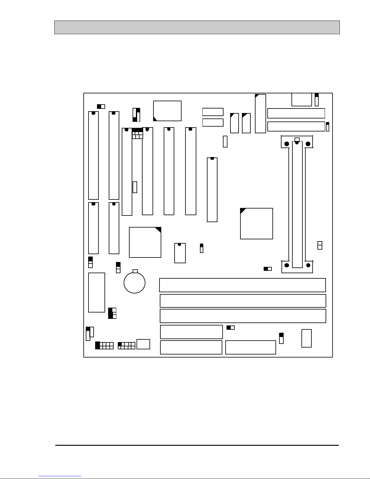
1.2 MAINBOARD LAYOUT
RS
HL
CN1
ATX POWER
BAT 1
CN 2
SYS. BIOS
+
-
AT POWER
DIMM 3
DIMM 2
SLOT1
LPT
JP1
CN16 WOL
TL
SL
PW
PWR-LED
K BLOCK
SPK
JP 7
JP 8
JP 9
JP 4
JP 5
JP 3
JP 1 1
CN 8
CN 17
DIMM 1
FDCIDE 1
IDE 2
HL
RS
CN6
USB1
CN7
USB2
CN 5
CN 15
CN 14
COM1
COM2
JP100
IR/FIR
JP 11
JP 6
CN 13
CP U FAN
JP13
JP133
JP 1 4

VIA 693/693A AT MAINBOARD INTRODUCTION
1-3
1.3 SPECIFICATION
¥ CPU
Intel® Pentium™ II or Pentium™ !!! 233, 266, 300, 333. 350, 366, 400, 433, 450,
466, 500MHz and higher speed processors
¥ CPU VCC
Switching mode Voltage Regulator onboard, supports +1.30V DC through +3.5V
DC CPU Core Voltage.
Note : The CPU Core Voltage will be Detected and adjusted automatically by the
mainboard, so there is no jumper setting required to select the CPU
voltage.
¥ WORD SIZE
Data Path : 8-bit, 16-bit, 32-bit, 64-bit
Address Path : 32-bit
¥ PC SYSTEM CHIPSET
PC133: VIA693A and 596B chipset
PC100: VIA693 and 596A Chipset (596B optional )
¥ SUPER I/O CHIPSET
W83977EF/TF or CTF/ATF (optional)
¥ FRONT SIDE BUS FREQUENCY
VIA693A : 66 MHz 100MHz and 133MHzselectable.
VIA693: 66 MHz and 100MHz selectable.
¥ MEMORY
Three 168-pin DIMM sockets, Maximum 768 MB with ECC.
CACHE :512KB pipelined burst SRAM in Pentium™ II, Pentium™ !!! processor.
¥ BIOS
AWARD System BIOS. 256KB x 8 Flash ROM
(Supports Plug & Play, ACPI, DMI and Green functions).
¥ EXPANSION SLOTS
AGP Slots : 32-bit x 1 (Supports 1x or 2x AGP graphics cards)
PCI Slots : 32-bit x 4 ( All Master/Slave, PCI 2.1 Compliant )
ISA Slots : 16-bit x 2 (One of the slot is PCI/ISA shared)

VIA 693/693A AT MAINBOARD INTRODUCTION
1-4
¥ WOL PORTS
One WOL connector supports Wake-On-LAN (WOL up-designed)
¥ USB PORTS
Two Universal Serial Bus (USB) ports.
¥ IDE PORTS
Two channels of Ultra DMA/33 (or UDMA/66) Bus Master IDE ports, which will
support up to 4 IDE devices like IDE hard disk, ATAPI CD-ROM etc. The IDE
ports can be programmed to support PIO Mode 4, DMA mode 2 and Ultra
DMA/33.
Note: When the chipset on U11 is the VIA596A, you may see the following
message on the screen if you are using the UDMA/66 HDD.
"Primary IDE Channel no 80 conductor cable installed. …"
Basically, this VIA596A mainboard will work with UDMA/66 HDD, but the
performance will be reduced because it does not support the new transfer protocol.
¥ SUPER I/O PORTS
1. Two high speed NS16C550 compatible serial ports (UARTs).
2. One parallel port, supports SPP/EPP/ECP mode.
3. One Floppy Disk Control port.
¥ IR PORT
One HPSIR and ASKIR or FasterIR (optional) compatible IR port.
One Consumer IR port (optional)
¥ MOUSE AND KEYBOARD
One PS/2™ mouse connector, One AT type keyboard connector.
(PS/2™ type keyboard connector is optional )
¥ HARDWARE DOCTOR ™ (optional)

VIA 693/693A AT MAINBOARD INTRODUCTION
1-5
Winbond W83783S (U2) is designed on the board to monitor hardware healthy
status like system voltage, system temperature, and cooling fans. When the CPU is
over heated, the system BIOS will tell the system board to give a series of beeping
alarm and then slow down the CPU speed so that you can take proper action to
prevent damage to your system. When you hear the beeping alarm, be sure to turn
the power off and open the chassis immediately, check on the cooling fans
(especially the CPU cooling fan ) to see whether it is working properly or not. If
you don’t know how to handle it, send the PC system to your dealer for technical
support.
This mainboard also provides the hardware monitoring program so that you can
monitor the healthy status of your PC system. When you find there is the Winbond
W83783S (U2) is installed on the board, you can run the hardware monitoring
program and then it will inform you the system status all the time.
¥ ACPI ( This feature is valid only when ATX power supply is connected )
Advanced Configuration and Power Interface (ACPI) function is strongly
recommended by PC’98 because it will let you have many additional features and
that will make your PC system becomes very friendly and convenient. Followings
are the ACPI features designed on the board:
1. Power on the system by panel-switch
2. Power on the system by LAN signal.( Wake On LAN )
3. Power on the system by Keyboard (Optional).
4. Power on the system By PS/2 Mouse key click (Optional)
5. CPU cooling fan auto-off during Suspend state.
6. Resumed by Modem ring-in, RTC alarm, .... etc..
7. Power on the system by RTC alarm (optional)
8. Power on the system by modem Ring-in signal (optional)
9. Supports Full-On/Doze/Standby/Suspend operating modes.
10. Power off (soft-off) by OS (active with ATX SPS only) or Panel-switch.
¥ DIMENSION
4-layers PCB, 220mm x 240mm (Baby-AT Form-Factor)..
¥ ENVIRONMENT LIMIT
1. Operating Temperature : 10 to 40. (50 to 104)
2. Required Airflow : 50 linear feet per minute across CPU.
3. Storage Temperature : - 40 to 70. (- 40 to 158)

VIA 693/693A AT MAINBOARD INTRODUCTION
1-6
4. Humidity : 0 to 90% non-condensing.
5. Altitude : 0 to 10,000 feet.

VIA 693/693A AT MAINBOARD INSTALLATION
2-1
2. INSTALLATION
2.1 UNPACKING
The mainboard contains the following components in the package. Please inspect the
following contents and confirm that everything is there in the package. If anything is
missing or damaged, call your supplier for instructions before proceeding.
l This mainboard.
l One USER‘S MANUAL.
l One Cable set for peripheral devices.
l One Pentium™ II Processor Retention Mechanism (RM).
l One CD diskette for device drivers and utility programs.
This mainboard contains electrostatic sensitive components and it can be easily
damaged by static electricity. So please leave it sealed in the original packing until
when installing.
A grounded anti-static mat is recommended when unpacking and installation. Please
also attached an anti static wristband to your wrist and have it grounded to the same
point as the anti-static mat.
After the opening of the mainboard carton, please observe the mainboard carefully to
make sure there is no shipping and handling damage before you can start to install the
PC system.

VIA 693/693A AT MAINBOARD INSTALLATION
2-2
2.2 AMAZING WAYS TO POWER ON THE PC SYSTEM
Basically, you can connect either AT or ATX power supply to this mainboard. When
the ATX power supply is connected, there are many ways to power on the system.
Please read the following description for the details.
POWER BUTTON
The power button (PW switch) on the front panel is not only for power-on and
power-off the PC system. When the ATX type power supply is connected to the
mainboard, it can be programmed by COMS setup program and it has different
features. Please refer to Section 3-2 (page 3-12, 3~13) for the detail of function
description.
¨ KEYBOARD PASSWORD or HOT KEY (optional)
When ATX type power supply is used with this mainboard, you may enter your
personal password or a combination of hot key in the CMOS setup program so that
you can use the keyboard password or hot key to power on your system. When the
system power is off, This mainboard has the stand-by 5V voltage active and it will
keep scanning the keyboard status waiting for the correct password or hot key input
to turn on the system power. Without the correct password or hot key, no one else
can turn on the PC system ( neither by the power button ).
There are two ways to power-on the PC system by keyboard, they are “Password”
and “Hot KEY”:

VIA 693/693A AT MAINBOARD INSTALLATION
2-3
¨ PS/2™ MOUSE KEY CLICK (optional)
When you have a PS/2™ mouse and ATX power supply connected to the system,
you may change the setup in the BIOS and use the mouse click to turn on the PC
system power.
To use the mouse key to turn on the PC system power, the mouse click must be done
quickly and continually. Basically, 2-5 quick clicks on the mouse key ( left key or
right key ) will turn the power immediately.
In order to activate the mouse key feature, you will have to reboot the PC system
after the BIOS setting and wait until the POST (Power On Self Test) is completed.
Having finished the procedure, you may use the mouse key to power-on the PC
system afterward..
Note: This feature is not available on the COM (serial) port mouse.
¨ RTC ALARM (this feature only work with ATX power supply)
PC system can be waked up by the RTC setting in the CMOS. You can set the
alarming date and time in the RTC memory, When RTC alarms, the PC system will
be triggered and wakes up automatically.
Enable the “RTC Alarm Resume” selection in the BIOS setup utility, and then input
the accurate date and time in following fields. (the “RTC Alarm Resume” is located
in the “POWER MANAGEMENT SETUP”, please refer to Section 4-7), Having
stored the RTC alarm setting, the PC system will be turned on automatically
according to the date and time which is recorded in the CMOS memory.
When you have finished the BIOS setting, you have to reboot the PC system and
wait for the POST (Power On Self Test) is completed to enable the RTC alarm.

VIA 693/693A AT MAINBOARD INSTALLATION
2-4
¨ MODEM RING-IN ( For ATX power supply only)
This mainboard can be triggered by a modem ring-in signal. When you have a
external modem installed, you can use it to power on the PC system. When there is
the incoming message from the external modem, the PC system will be triggered by
the ring-in signal and wake up automatically to receive the message for you.
In order to use the ring-in signal to wake up your PC system, you will have to use
the EXTERNAL MODEM and have it connected to one of the Serial Ports (COM1
or COM2). When the system power is off, this mainboard will continue to detect the
serial port status. When it detects the ring-in signal from the serial port, the system
power will be turned on and start to receive the incoming messages automatically.
To enable the Modem Ring-In feature, you have to run the BIOS setup utility and
enable the “Modem or LAN resume” option (it is in the “POWER MANAGEMENT
SETUP”, please refer to Section 4.7 for the settings). Having completed the BIOS
setup, you have to reboot the PC system so that BIOS can verify the setting. (the
“DMI pool data” will be verified by the BIOS when loading the operating system).
Simply speaking, shut down the PC system and then re-start the system. The modem
ring-in feature will be enabled when the operation system has been loaded.
Note: This function is not available when using the internal MODEM card.
¨ WAKE ON LAN ( WOL ) ( For ATX power supply only)
There is a WOL connector CN14 (see Section 3-2) on the mainboard which is
designed to connect to the signal from a LAN card which supports the Wake On
LAN feature. When such LAN card is installed, you may turn on the PC system
from your remote server and monitor the PC status.
To enable this feature, you will have to use the BIOS setup utility to enable the
“Modem or LAN resume” (it is located at “POWER MANAGEMENT SETUP”,
please refer to Section 4-7 for the settings). Having completed the BIOS setup, you
have to reboot the PC system so that BIOS can verify the setting. ( the “DMI pool
data” will be verified by the BIOS when loading the operating system). Simply
speaking, reboot the PC system, the Wake On LAN feature will be enabled when the
operation system has been loaded
Note: This function will be disabled if you turn off the power before the system
can verify the DMI pool data.

VIA 693/693A AT MAINBOARD INSTALLATION
2-5
2.3 POWER OFF THE PC SYSTEM
1. When ATX power supply is connected.
There are two ways to power off the system. They are “Shut Down by Power
Button” and “ Shut Down by OS”. (such as Windows® 95 and Windows® 98,
you can choose the Shut Down from the file menu and the system will be
powered off immediately ).
2. When AT power supply is connected.
You can not use the OS to shut down the PC system, you can use only the power
switch to turn the system power off.
VIA 693/693A AT MAINBOARD HARDWARE SETUP
3-1
3. HARDWARE SETUP
Before you can start to install this mainboard, some hardware settings is required
to make sure it will work perfectly with the component which you are going to
install in your PC system. To configure this mainboard is a simple task, only a few
jumpers, connectors, cables and sockets need to be selected and configured.
Please refer to the following sections for the settings.
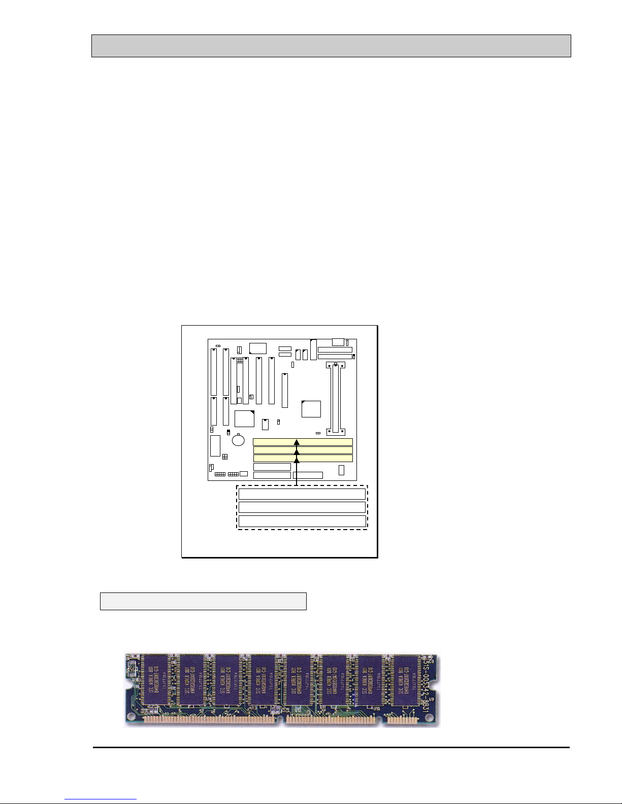
3.1 INSTALLING THE DRAM MODULES
This mainboard has three DIMM sockets designed on the mainboard and you can use
the single-side or double-side DIMM module on the mainboard.
RS
HL
BAT 1
+
-
DRAM Subsystem Diagram
DIMM 3 ( BANK4+ BANK5 )
DIMM 2 ( BANK2 + BANK3 )
DIMM 1 ( BANK0 + BANK1 )
Installation of DIMM modules:
1. Outlook of DIMM modules:
VIA 693/693A AT MAINBOARD HARDWARE SETUP
3-2
( Single-Side DIMM module )
( Double-Side DIMM Module )
2. Minimum one DIMM module must be installed on the mainboard.
3. For PC133 M/B (VIA693A chipset). please use 3.3V PC-133 DIMM module.
4. For PC100 M/B (VIA693 chipset), please use 3.3V PC-100 DIMM module.
5. You can use single side or double side DIMM module on this mainboard.
6. Please install the DIMM module starting from DIMM2 first.
If your DIMM module does not have the parity bit, please
don't enable the Parity/ECC check feature in the BIOS setup.
3.2 CONNECTORS
The connectors on mainboard will be used to connect the accessories or peripheral
devices (such as power, mouse, printer,...etc.). Followings are the connectors with
its description and pin assignment which is designed on the mainboard.
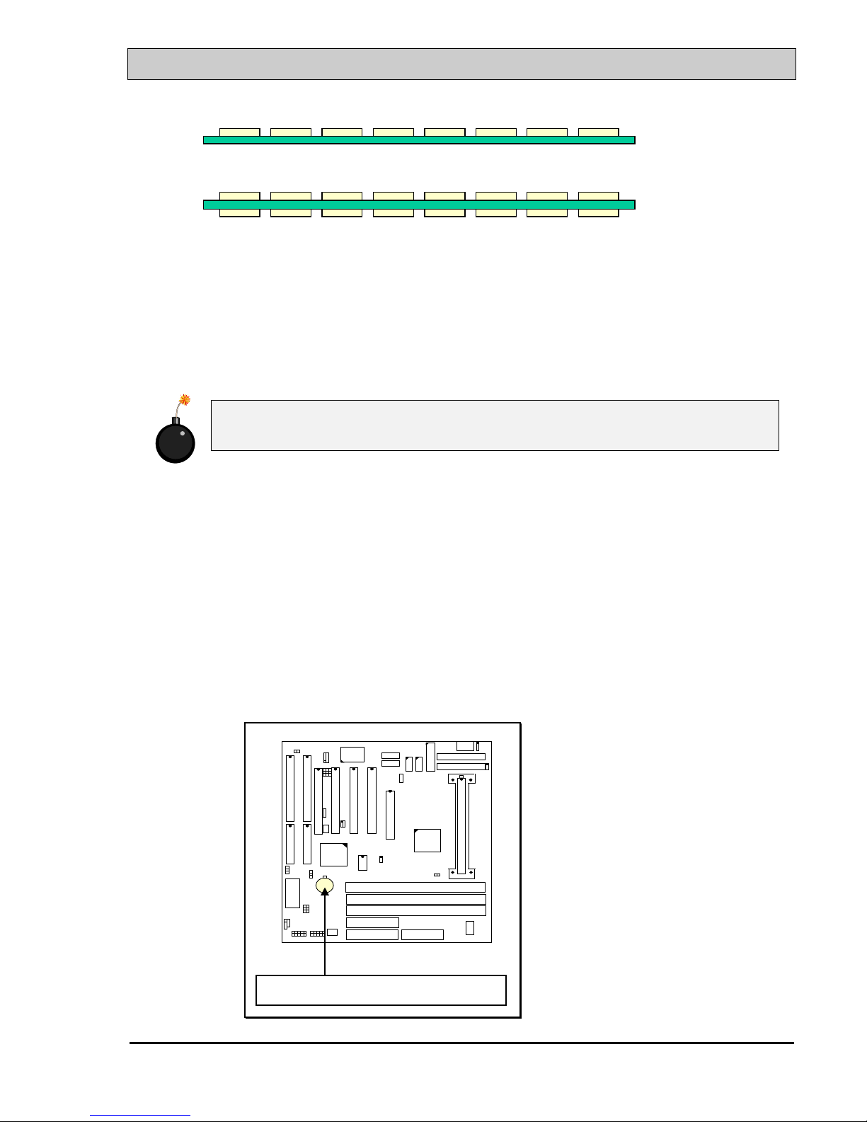
BAT1: Battery Socket (Use the 3 Volts Lithium battery : CR2032)
RS
HL
BAT 1
+
-
DIMM 3
DIMM 2
DIMM 1
FDCIDE 1
IDE 2
BAT1: Battery Socket
VIA 693/693A AT MAINBOARD HARDWARE SETUP
3-3
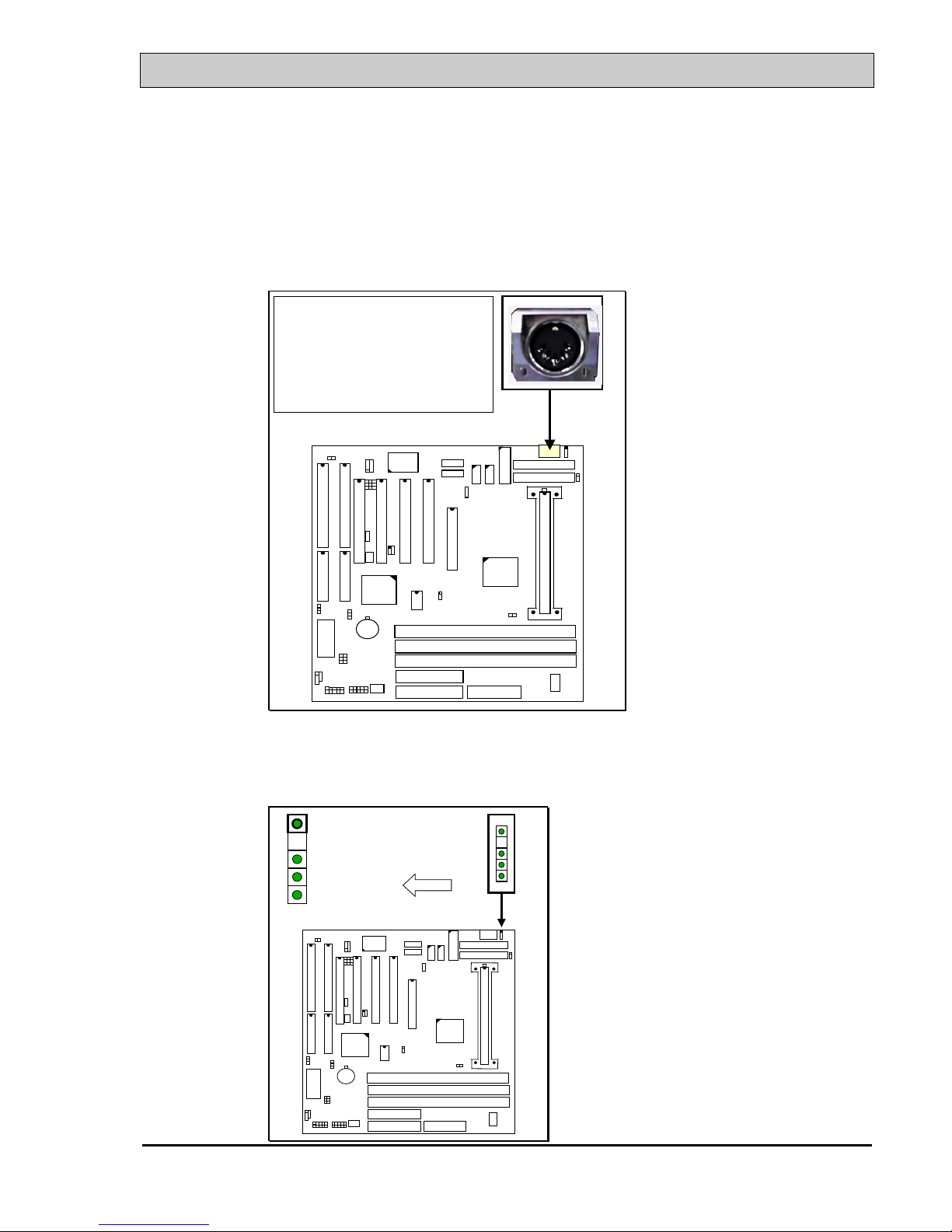
(A) CN1: Keyboard Connectors
Either the PS/2 (CN20) type or the AT (CN1) type keyboard connector can be
installed here, ( only one connector can be installed) The factory default is the AT
type connector installed on the board. When the AT type K/B installed on the
board, the PS/2 type (CN20) become invisible.
RS
HL
BAT 1
+
-
DIMM 3
DIMM 2
DIMM 1
FDCIDE 1
IDE 2
K/B CONNECTORS:
Either PS/2 or AT type K/B connector
can be installed on the mainboard.
Basically, these two connectors share
the same space, so there is only one
connector can be installed.
Default: AT type connector installed.
(B) CN2: PS/2 Mouse Connector
RS
HL
BAT 1
+
-
DIMM 3
DIMM 2
DIMM 1
FDCIDE 1
IDE 2
1
2
3
4
5
Mouse Data
No Connection
Ground
+5V DC
Mouse Clock
CN 2
 Loading...