

Page 1

AW-CB250NF
IEEE 802.11 2x2 MU-MIMO a/b/g/n/ac
Wireless LAN + Bluetooth 5.0 M.2 2230
Module
User’s Manual
Version 0.1
- 1 -
Page 2

Federal Communication Commission Interference Statement
This equipment has been tested and found to comply with the limits for a Class B digital device,
pursuant to Part 15 of the FCC Rules. These limits are designed to provide reasonable
protection against harmful interference in a residential installation. This equipment generates,
uses and can radiate radio frequency energy and, if not installed and used in accordance with
the instructions, may cause harmful interference to radio communications. However, there is no
guarantee that interference will not occur in a particular installation. If this equipment does
cause harmful interference to radio or television reception, which can be determined by turning
the equipment off and on, the user is encouraged to try to correct the interference by one of the
following measures:
Reorient or relocate the receiving antenna.
Increase the separation between the equipment and receiver.
Connect the equipment into an outlet on a circuit different from that to which the receiver is
connected.
Consult the dealer or an experienced radio/TV technician for help.
FCC Caution: Any changes or modifications not expressly approved by the party responsible for
compliance could void the user’s authority to operate this equipment.
This device complies with Part 15 of the FCC Rules. Operation is subject to the following two
conditions: (1) This device may not cause harmful interference, and (2) this device must accept
any interference received, including interference that may cause undesired operation.
This device is restricted for indoor use.
FCC Radiation Exposure Statement:
This equipment complies with FCC radiation exposure limits set forth for an uncontrolled
environment. This equipment should be installed and operated with minimum distance 20cm
between the radiator & your body.
IMPORTANT NOTE:
This module is intended for OEM integrator. This module is only FCC authorized for the
specific rule parts listed on the grant, and that the host product manufacturer is
responsible for compliance to any other FCC rules that apply to the host not covered by
the modular transmitter grant of certification. The final host product still requires Part 15
Subpart B compliance testing with the modular transmitter installed.
Additional testing and certification may be necessary when multiple modules are used.
USERS MANUAL OF THE END PRODUCT:
In the user’s manual of the end product, the end user has to be informed to keep at least
20cm separation with the antenna while this end product is installed and operated. The
end user has to be informed that the FCC radio-frequency exposure guidelines for an
uncontrolled environment can be satisfied.
The end user has to also be informed that any changes or modifications not expressly
approved by the manufacturer could void the user's authority to operate this equipment.
- 2 -
Page 3

Type
Antenna Vendor
Part Number
Peak Gain
Dipole
Invax System
Technology Corp.
AN2450-5511BRS-SMASFR83100B-4AX00I
2.14 dBi @ 2400~2500MHz
3.61 dBi @ 5150~5850MHz
PIFA
MAG. LAYERS
MSA-4008-25GC1-A2
2.98 dBi @ 2400~2500MHz
5.16 dBi @ 4900~5900MHz
This device complies with Part 15 of FCC rules. Operation is subject to the following two
conditions: (1) this device may not cause harmful interference and (2) this device must
accept any interference received, including interference that may cause undesired
operation.
LABEL OF THE END PRODUCT:
The final end product must be labeled in a visible area with the following "Contains TX
FCC ID: TLZ-CB250NF".
This device complies with Part 15 of FCC rules. Operation is subject to the following two
conditions: (1) this device may not cause harmful interference and (2) this device must
accept any interference received, including interference that may cause undesired
operation.
- 3 -
Page 4

Document
release
Date
Modification
Initials
Approved
Version 0.1
2019/10/01
Initial version
Josh Lin
Patrick Lin
Revision History
- 4 -
Page 5

Table of Contents
1. GENERAL DESCRIPTION ................................................................................................... 6
1.1 PRODUCT OVERVIEW AND FUNCTIONAL DESCRIPTION ............................................... 6
1.2 KEY FEATURE ...................................................................................................................... 7
1.3 SPECIFICATIONS TABLE .................................................................................................... 7
2. ELECTRICAL CHARACTERISTIC ...................................................................................... 9
3. HOST INTERFACES .......................................................................................................... 11
3.1 PCI EXPRESS INTERFACE ................................................................................................ 11
3.1.1 DIFFERENTIAL TX OUTPUT ELECTRICALS ............................................................. 11
3.1.2 DIFFERENTIAL RX OUTPUT ELECTRICALS ............................................................ 12
3.2 USB INTERFACE ................................................................................................................ 12
3.2.1 USB 2.0 DEVICE INTERFACE DESCRIPTION ........................................................... 13
3.2.2 USB 2.0 DEVICE FUNCTIONAL DESCRIPTION ........................................................ 13
3.3 HIGH-SPEED UART INTERFACE ....................................................................................... 13
3.3.1 UART INTERFACE SIGNAL DESCRIPTION .............................................................. 14
3.3.2 UART INTERFACE FUNCTIONAL DESCRIPTION ..................................................... 14
3.4 PCM INTERFACE ............................................................................................................... 15
3.4.1 PCM TIMING SPECIFICATION – MASTER MODE ..................................................... 15
3.4.2 PCM TIMING SPECIFICATION – SLAVE MODE ........................................................ 17
4. PIN DEFINITION................................................................................................................. 18
5. MECHANICAL INFORMATION.......................................................................................... 21
5.1 PACKAGE OUTLINE DRAWING ........................................................................................ 21
- 5 -
Page 6

1. General Description
1.1 Product Overview and Functional Description
AzureWave Technologies, Inc. introduces the IEEE 802.11ac/a/b/g/n 2X2 MU-MIMO WLAN &
Bluetooth NGFF module --- AW-CB250NF. The module is targeted to mobile devices including
Notebook, TV, Tablet and Gaming Device which need small package module, low power consumption,
multiple interfaces and OS support. By using AW-CB250NF, the customers can easily enable the Wi-Fi,
and BT embedded applications with the benefits of high design flexibility, short development cycle,
and quick time-to-market.
Compliance with the IEEE 802.11ac/a/b/g/n standard supporting 802.11ac Wave 2, the AW-CB250NF
uses Direct Sequence Spread Spectrum (DSSS), Orthogonal Frequency Division Multiplexing (OFDM),
DBPSK, DQPSK, CCK and QAM baseband modulation technologies. A high level of integration and full
implementation of the power management functions specified in the IEEE 802.11 standard minimize the
system power requirements by using AW-CB250NF. In addition to the support of WPA/WPA2 and WEP
64-bit and 128-bit encryption, the AW-CB250NF also supports the IEEE 802.11i security standard
through the implementation of Advanced Encryption Standard (AES)/Counter Mode CBC-MAC
Protocol (CCMP), Wired Equivalent Privacy (WEP) with Temporal Key Integrity Protocol (TKIP),
Advanced Encryption Standard (AES)/Cipher-Based Message Authentication Code (CMAC), and WLAN
Authentication and Privacy Infrastructure (WAPI) security mechanisms.
For the video, voice and multimedia applications the AW-CB250NF support 802.11e Quality of Service
(QoS). The device also supports 802.11h Dynamic Frequency Selection (DFS) for detecting radar
pulses when operating in the 5GHz range.
For Bluetooth operation, AW-CB250NF is Bluetooth 5.0 (supports Low Energy).
AW-CB250NF supports PCIE, USB 3.0/2.0, and high speed UART interfaces for WLAN and Bluetooth
to the host processor.
AW-CB250NF is suitable for multiple mobile processors for different applications with the support
cellular phone co-existence. AW-CB250NF module adopts Marvell’s latest highly-integrated dual-band
WLAN & Bluetooth SoC---88W8997. All the other components are implemented by all means to reach
the mechanical specification required.
- 6 -
Page 7

Model Name
AW-CB250NF
Product Description
IEEE 802.11 2x2 MU-MIMO a/b/g/n/ac Wireless LAN + Bluetooth 5.0 M.2
2230 type Module
WLAN Standard
IEEE 802.11 ac/a/b/g/n, Wi-Fi compliant
Bluetooth Standard
Bluetooth 5.0 complaint with Bluetooth 2.1+Enhanced Data Rate (EDR)
Host Interface
PCIe for WLAN, USB/UART for Bluetooth
Major Chipset
Marvell 88W8997
Dimension
22mm x 30mm x 2.3mm
Weight
TBD
Package
PCIe M.2 type 2230-S3-E
Operating Conditions
Voltage
3.3V+- 10%
Temperature
Operating: -40~ 85oC ; Storage: -55 ~ 125oC
Electrical Specifications
Frequency Range
2.4 GHz ISM radio band / 5 GHz Unlicensed National Information
Infrastructure (U-NII) band
1.2 Key feature
PCIe M.2 TYPE 2230-S3-E: 22mm(L) x 30mm(W) x 2.3 mm(H)
PCIe, USB 3.0/2.0 interfaces support for WLAN
USB 3.0/2.0, UART interfaces support for Bluetooth
High speed UART,PCM interfaces
Bluetooth 5.0 complaint with Bluetooth 2.1 + Enhanced Data Rate (EDR)
Audio Codec interface support
Cellular phone co-existence support (TBD)
Sub-meter accuracy Wi-Fi indoor locationing (802.11mc)
Multiple power saving modes for low power consumption
IEEE 802.11i for advanced security
Quality of Service (QoS) support for multimedia applications
Support China WAPI
Lead-free design
Support optional VIO level(3.3V or 1.8V)
1.3 Specifications Table
- 7 -
Page 8

Number of Channels
802.11a:
USA–36, 40, 44, 48, 52, 56, 60, 64, 100, 104, 108, 112, 116, 120, 124, 128, 132,
136, 140, 149, 153, 157, 161, 165
802.11b:
USA, Canada and Taiwan – 1~11
Most European Countries – 1~13
802.11g:
USA, Canada and Taiwan – 1~11
Most European Countries – 1~13
802.11n
BW20: Channel 1~13 (2412~2472)
BW40: Channel 3~9 (2422~2462)
802.11ac
BW20: 36, 40, 44, 48, 52, 56, 60, 64, 100, 104, 108, 112, 116, 120, 124, 128, 132,
136, 140, 149, 153, 157, 161, 165
BW40: 38, 46, 54, 62, 102, 110, 118, 126, 134, 151, 159
BW80: 42, 58, 106, 122, 138, 155
Modulation
DSSS, OFDM, DBPSK, DQPSK, CCK, 16-QAM, 64-QAM and 256-QAM for WLAN
GFSK (1Mbps), Π/4 DQPSK (2Mbps) and 8DPSK (3Mbps) for Bluetooth
Antenna Connector
Main Connector: WLAN Aux Connector: WLAN + BT
Medium Access Protocol
CSMA/CA with ACK
Data Rates
WLAN
802.11b: 1, 2, 5.5, 11Mbps
802.11a/g: 6, 9, 12, 18, 24, 36, 48, 54Mbps
802.11n: up to 150Mbps-single
802.11n: up to 300Mbps-2x2 MIMO
802.11ac:up to 192.6Mbps (20MHz channel)
802.11ac:up to 400Mbps (40MHz channel)
802.11ac:up to 866.7Mbps (80MHz channel)
Bluetooth
Bluetooth 5.0
Bluetooth 2.1+EDR data rates of 1,2, and 3Mbps
Power Consumption
TBD
Operating Range
Open Space: ~300m ; Indoor: ~100m for WLAN
Minimum 10 m indoor for Bluetooth
(The transmission speed may vary according to the environment)
Security
WAPI
WEP 64-bit and 128-bit encryption with H/W TKIP processing
WPA/WPA2 (Wi-Fi Protected Access)
AES-CCMP hardware implementation as part of 802.11i security standard
Operating System
Compatibility
Linux(Android) (More information please contact AzureWave FAE)
- 8 -
Page 9

Symbol
Parameter
Min
Typ
Max
Units
3.3V
Power supply voltage with respect to VSS
3.3
4.0
V
T
storage
Storage Temperature
-55 125
℃
Symbol
Parameter
Min
Typ
Max
Units
3.3V
Power supply voltage with respect to VSS
2.97
3.3
3.63 V TA
Ambient operating temperature
-40 85
℃
Symbol
Parameter
Min
Typ
Max
Units
CLK
Clock Frequency Range/accuracy
+-250ppm (initial, aging, temperature)
32.768
KHz
2. Electrical Characteristic
1.1 Absolute Maximum Ratings
1.2 Recommended Operating Conditions
1.3 Clock Specifications
1.3.1 External Sleep Clock Timing
External Sleep Clock is necessary for two reasons:
1. Auto frequency Detection
This is where the internal logic will bin the Ref clock source to figure out what is the reference clock frequency
is. This is done so no strapping is needed for telling 88W8997 what the ref clock input is.
2. Allow low current modes for BT to enter sleep modes such as sniff modes.
The AW-CB250NF external sleep clock pin is powered from the 3.3V voltage supply.
1.4 Reset Configuration
The AW-CB250NF is reset to its default operating state under the following conditions:
Power-on reset (POR)
Software/Firmware reset
External pin for power down (PDn)
- 9 -
Page 10

1.5 Power up Timing Sequence
- 10 -
Page 11

3. Host Interfaces
1.1 PCI Express Interface
1.1.1 Differential Tx Output Electricals
- 11 -
Page 12

1.1.2 Differential Rx Output Electricals
1.2 USB Interface
The USB device interface is compliant with the Universal Serial Bus Specification, Revision 2.0, April 27, 2000. A
USB host uses the USB cable bus and the USB 2.0 device interface to communicate with the chip. The main
features of the USB device interface include:
High/full speed operation (480/12 Mbps)
Suspend/host resume/device resume (remote wake-up)
Built-in DMA engine that reduces interrupt loads on the embedded processor and reduces the system bus
bandwidth requirement for serving the USB device operation
The USB 2.0 device interface is designed with 3.3V signal level pads.
- 12 -
Page 13

1.2.1 USB 2.0 Device Interface Description
Table shows the signal mapping between the AW -CB250NF and the USB Specification, Revision 2.0.
1.2.2 USB 2.0 Device Functional Description
The device controller uses internal Scatter/Gather DMA engine to transfer the transmit packet from internal SRAM
to USB and the receive packet from USB to internal SRAM. The Device IN Endpoint DMA (DIEPDMAn) and Device
OUT Endpoint DMA (DOEPDMAn) registers are used by the DMA engine to access the base descriptor. The
application is interrupted after the programmed transfer size extracted from the descriptors is transmitted or
received. By using registers, interrupts, and special data structures, the device controller can communicate with the
device controller driver (application/software) about bus states, host request, and data transfer status. The device
controller driver also has all of the routines to respond to the device framework commands issued by a USB host,
so it controls the attachment, configuration, operation, and detachment of the device.
1.3 High-Speed UART Interface
The AW-CB250NF supports a high-speed Universal Asynchronous Receiver/Transmitter (UART) interface,
compliant to the industry standard 16550 specification. High-speed baud rates are supported to provide the
physical transport between the device and the host for exchanging Bluetooth data. Table shows the rates
supported.
The UART interface features include:
FIFO mode permanently selected for transmit and receive operations
Two pins for transmit and receive operations
Two flow control pins
Interrupt triggers for low-power, high throughput operation
The UART interface operation includes:
Upload boot code to the internal CPU (for debug purposes)
- 13 -
Page 14

Support diagnostic tests
Support data input/output operations for peripheral devices connected through a standard UART interface
1.3.1 UART Interface Signal Description
Table shows the standard UART signal names on the device.
1.3.2 UART Interface Functional Description
1.3.2.1 Booting from UART
When booting from the UART, the AW-CB250NF device has the following requirements:
- 14 -
Page 15

1.3.2.2 UART as Test Port
Test diagnostic programs may be uploaded to the CPU through the UART interface. During execution, the
diagnostic program transmits performance and status information through the UART by performing a write to the
PBU address space designated to the UART.
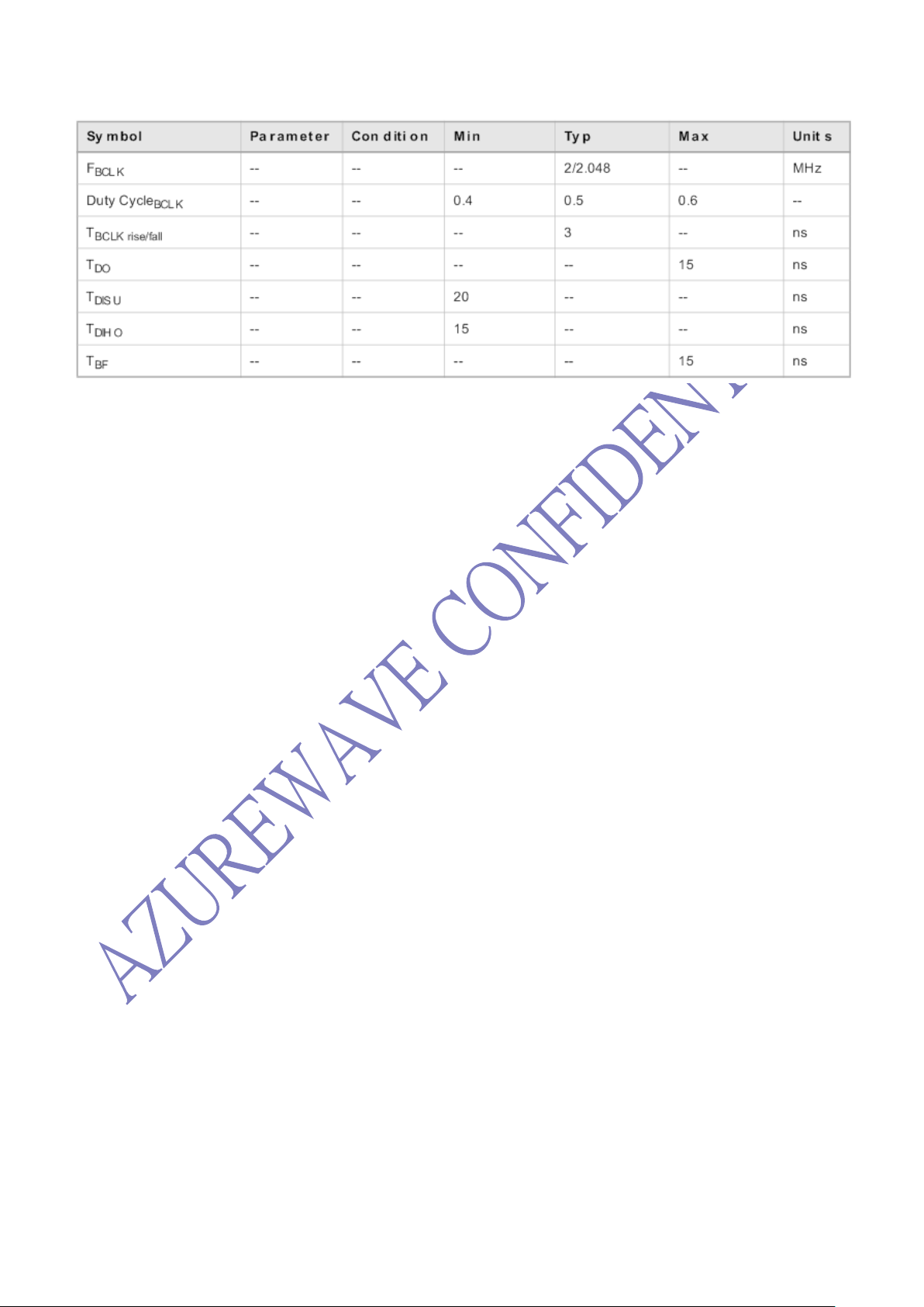
1.4 PCM Interface
1.4.1 PCM Timing Specification – Master Mode
- 15 -
Page 16
- 16 -
Page 17

1.4.2 PCM Timing Specification – Slave Mode
- 17 -
Page 18

Pin No
Definition
Basic Description
Type
Level
1
GND
System Ground Pin
2
3.3V
3.3V VBAT system power supply input
I
3.3V 3 USB_DP
USB Serial Differential Data Positive
I/O
3.3V 4 3.3V
3.3V VBAT system power supply input
I
3.3V 5 USB_DN
USB Serial Differential Data Negative
I/O
3.3V 6 WLAN_LED
GPIO[2] (output) for WLAN LED
O
3.3V
7
GND
System Ground Pin
8
GPIO[6]/PCM_CLK
GPIO[6] (input/output)
I/O
VIO
9
NC
NC
10
GPIO[7]/PCM_SYNC
GPIO[7] (input/output)
I/O
VIO
11
NC
NC
12
GPIO[4]/PCM_IN
GPIO[4] (input/output)
O
VIO
13
NC
NC
14
GPIO[5]/PCM_OUT
GPIO[5] (input/output)
I
VIO
15
NC
NC
16
BT_LED
GPIO[3] (output) for BT LED
O
3.3V
17
NC
NC
18
GND
System Ground Pin
19
NC
NC
20
GPIO[13]/UART WAKE_N
GPIO[13] for UART WAKE_N (output)
O
VIO
21
NC
NC
22
GPIO[8]/UART RXD
UART_SOUT (output)
O
VIO
23
PDn
Full Power Down (input) (active low)
I
1.8V
24
Connector Key
25
Connector Key
26
Connector Key
27
Connector Key
28
Connector Key
29
Connector Key
30
Connector Key
31
Connector Key
32
GPIO[9]/UART TXD
UART_SIN (input)
I
VIO
33
GND
System Ground Pin
34
GPIO[11]/UART_CTS
UART_RTSn (output)
O
VIO
*35
PCIE_RX_P/USB3_RX_P*
PCI Express Receive Data—Positive / USB 3.0 RX_P*
I
VIO
4. Pin Definition
- 18 -
Page 19

36
GPIO[10] ]/UART_RTS
UART_CTSn (input)
I
VIO
*37
PCIE_RX_N/USB3_RX_N*
PCI Express Receive Data—Negative / USB 3.0 RX_N*
I
VIO
38
NC
NC
39
GND
System Ground Pin
40
NC
NC
*41
PCIE_TX_P/USB 3_TX_P*
PCI Express Transmit Data—Positive / USB 3.0 TX_P*
O
VIO
*42
BT_WAKE*
Host to UART_BT wake up*
I
VIO
*43
PCIE_TX_N/USB 3_TX_N*
PCI Express Transmit Data—Negative / USB 3.0 TX_N*
O
VIO
44
COEX3
NC
45
GND
System Ground Pin
46
COEX2
NC
47
PCIE_RCLK_P
PCI Express Differential Clock Input—Positive
I
VIO
48
COEX1
NC
49
PCIE_RCLK_N
PCI Express Differential Clock Input—Negative
I
VIO
50
SLP_CLK
32.768KHz external clock
I
VIO
51
GND
System Ground Pin
52
PCIE_PERST_N
PCIe host indication to reset the device (input) (active low)
I
VIO
53
PCIE_CLKREQn
PCIe clock request (input/output) (active low)
I/O
VIO
*54
GPIO[1]/PDn*
USB_VBUS_ON power valid indication/ PDn (optional)*
I
VIO
55
PCIE_WAKEn
PCIe wake signal (output) (active low)
O
VIO
56
PCIE_DISABLE_N
PCIe host indication to disable the WLAN function of the device
I
VIO
57
GND
System Ground Pin
58
NC
NC
59
Reserved
NC
60
NC
NC
61
Reserved
NC
62
NC
NC
63
GND
System Ground Pin
64
NC
NC
I 65
NC
NC
I 66
NC
NC
67
NC
NC
I 68
NC
NC
69
GND
System Ground Pin
70
NC
NC
71
NC
NC
72
3.3V
3.3V VBAT system power supply input
I
VIO
73
NC
NC
- 19 -
Page 20

74
3.3V
3.3V VBAT system power supply input
I
VIO
75
GND
System Ground Pin
Notes:
1. PCIE Impedance targets: Single-ended Z of 60 ohms +- 15% . Differential Impedance of ~100 ohm +- 20%.
2. USB Impedance targets: D+/D- are differential and should have 90ohms impedance.
3. * Implement by different hardware version.
4. Below table shows the configuration pins as host interface configuration input. (Default as PCIE/USB)
- 20 -
Page 21

5. Mechanical Information
5.1 Package Outline Drawing
- 21 -
 Loading...