

AZMIC AZ3267 Datasheet
AZ3267
2.5Gbps Transimpedance Amplifier
1630 S. STAPLEY DR., SUITE 125 • MESA, ARIZONA 85204 • USA • (480) 962-5881 • FAX (480) 890-2541
www.azmicrotek.com
ARIZONA MICROTEK, INC.
FEATURES
• 1900 MHz Bandwidth
• 1 mA Input Overload
• 11 pA/Hz
1/2
Noise Density
• Single 3.0V to 3.6V or 4.5V to 5.5V Supply
• Internal DC Restoration Capacitor
• Direct Replacement for MAX3267
DESCRIPTION
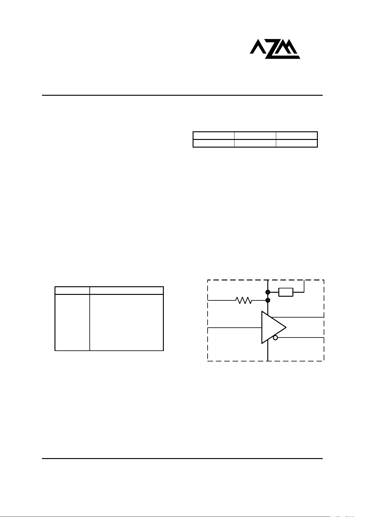
The AZ3267 is a transimpedance amplifier for 2.5Gbps fiber optic receivers. The part operates from a single
3.0V to 3.6V or 4.5V to 5.5V supply. Photodiode bias is provided via a 1.5kΩ resistor from V
CC
.
DC restoration is built in, with no external compensation capacitor required. The DC restoration can be disabled
for testing by pulling the FILTER pin to ground potential.
If the part is operated using the V
CC5
supply pin, the VCC pin should be bypassed to ground with a capacitor of at
least 0.1µf.
PACKAGE AVAILABILITY
PACKAGE PART NO. MARKING
DIE AZ3267 N/A
PAD DESCRIPTION
NAME FUNCTION
VCC Supply Voltage 3.0 to 3.6V
V
CC5
Supply Voltage 4.5 to 5.5V
IN Photodiode Input
FILTER
Bias Voltage Via 1.5kΩ
Resistor
GND Ground
OUT- Inverting Output
OUT+ Noninverting Output
BLOCK DIAGRAM
IN
1.5 K
OUT+
OUT-
V
CC5
V
CC
FILTER
GND
AZ3267
March 2002 * REV - 3 www.azmicrotek.com
2
Absolute Maximum Ratings are those values beyond which device life may be impaired.
Symbol Character Value Unit
V
CC2
DC Supply Voltage (Referenced to GND) 6.0 V
TA Operating Temperature Range (In Free-Air) -40 to +85
°C
T
STG
Storage Temperature Range -65 to +150
°C
IN Current
±3
mA
FILTER Current
±3
mA
ELECTRICAL CHARACTERISTICS (V
CC
= 3.0V to 3.6V or V
CC5
= 4.5 to 5.5V; 100Ω load between OUT+ and OUT-)
Symbol Characteristic Min Typ Max Unit Condition
Input Bias Voltage 0.70 0.81 0.93 V
ICC Power Supply Current 21 35 mA
Transimpedance 1540 1900 2330
Ω
40µA p-p input
Ro Output Impedance 50
Ω
Per output pin
Maximum Differential Output Voltage 185 250 415 mV p-p 1 mA p-p input
Filter Resistor 1220 1500 1860
Ω
AC Input Overload 1.0 mA p-p
DC Input Overload 0.65 mA
Input Referred Noise Density 11 pA/Hz½
Small Signal Bandwidth 1530 1900 2420 MHz
≤40 uA p-p
Low Frequency Cutoff 44 kHz
-3 dB, input ≤40 uA p-p
Power Supply Rejection Ratio 50 dB Output referred, f < 2 MHz
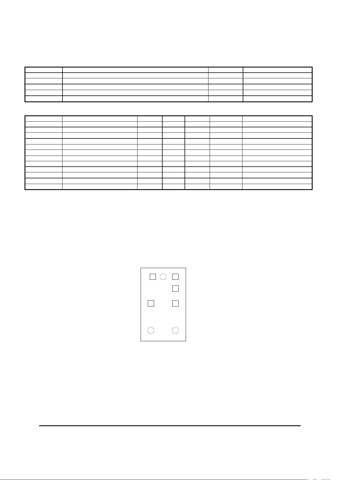
1355-002
OUT-
OUT+
GND
GND
VCC
VCC5
IN
FILTER
Die Size: 1260 x 800 µm
Pad Size: 85 x 85 µ
 Loading...