

AZMIC AZ10EP16VSTR2, AZ10EP16VSTR1, AZ10EP16VST, AZ10EP16VSLR2, AZ10EP16VSLR1 Datasheet
...
AZ10EP16VS
AZ100EP16VS
ECL/PECL Differential Receiver with Variable Output Swing
1630 S. STAPLEY DR., SUITE 125 • MESA, ARIZONA 85204 • USA • (480) 962-5881 • FAX (480) 890-2541
www.azmicrotek.com
ARIZONA MICROTEK, INC.
FEATURES
• Silicon-Germanium for High Speed Operation
• 150ps Typical Propagation Delay
• AZ100EP16VS Functionally Equivalent to ON
Semiconductor MC100EP16VS at 3.3V
• Available in a 3x3mm MLP Package
DESCRIPTION
The AZ10/100EP16VS is a Silicon–Germanium (SiGe) differential receiver with variable output swing. The
EP16VS has functionality and output transition times similar to the EP16, with an input that controls the amplitude
of the Q/Q¯ outputs.
The operational range of the EP16VS control input, V
CTRL
, is from V
REF
(full swing) to VCC (min. swing).
Maximum swing is achieved by leaving the V
CTRL
pin open or tied to VEE. Simple control of the output swing can be
obtained by a variable resistor between the V
REF
and VCC pins, with the wiper driving V
CTRL
. Typical application
circuits and results are described in this Data Sheet.
The EP16VS provides a V
REF
output for a DC bias for AC coupling to the device. The V
REF
pin should be used
only as a bias for the EP16VS as its current sink/source capability is limited. Whenever used, the V
REF
pin should
be bypassed to ground via a 0.01µF capacitor.
Under open input conditions for D/D¯, the Q/Q¯ outputs are not guaranteed.
NOTE: Specifications in ECL/PECL tables are valid when thermal equilibrium is established.
PACKAGE AVAILABILITY
PACKAGE PART NO. MARKING
MLP 8 AZ10EP16VSL AZM16E
MLP 8 T&R AZ10EP16VSLR1 AZM16E
MLP 8 T&R AZ10EP16VSLR2 AZM16E
MLP 8 AZ100EP16VSL AZM16F
MLP 8 T&R AZ100EP16VSLR1 AZM16F
MLP 8 T&R AZ100EP16VSLR2 AZM16F
SOIC 8 AZ10EP16VSD AZM10EP16VS
SOIC 8 T&R AZ10EP16VSDR1 AZM10EP16VS
SOIC 8 T&R AZ10EP16VSDR2 AZM10EP16VS
SOIC 8 AZ100EP16VSD AZM100EP16VS
SOIC 8 T&R AZ100EP16VSDR1 AZM100EP16VS
SOIC 8 T&R AZ100EP16VSDR2 AZM100EP16VS
TSSOP 8 AZ10EP16VST AZTP16VS
TSSOP 8 T&R AZ10EP16VSTR1 AZTP16VS
TSSOP 8 T&R AZ10EP16VSTR2 AZTP16VS
TSSOP 8 AZ100EP16VST AZHP16VS
TSSOP 8 T&R AZ100EP16VSTR1 AZHP16VS
TSSOP 8 T&R AZ100EP16VSTR2 AZHP16VS
AZ10EP16VS
AZ100EP16VS
November 2001 * REV - 3 www.azmicrotek.com
2
Absolute Maximum Ratings are those values beyond which device life may be impaired.
Symbol Characteristic Rating Unit
VCC PECL Power Supply (VEE = 0V) 0 to +4.5 Vdc
VI PECL Input Voltage (V
EE
= 0V) 0 to +4.5 Vdc
VEE ECL Power Supply (VCC = 0V) -4.5 to 0 Vdc
VI ECL Input Voltage (VCC = 0V) -4.5 to 0 Vdc
I
OUT
Output Current --- Continuous
--- Surge
50
100
mA
TA Operating Temperature Range -40 to +85
°C
T
STG
Storage Temperature Range -65 to +150
°C
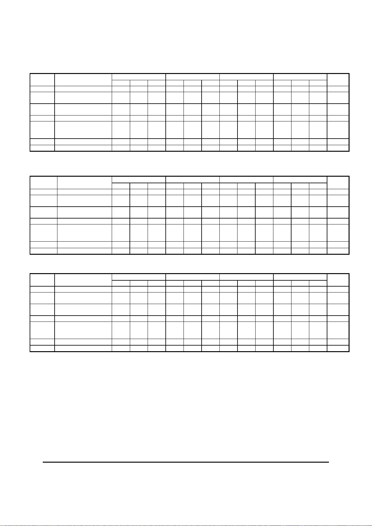
10K ECL DC Characteristics (VEE = -3.0V to -3.6V, VCC = GND)
-40°C 0°C 25°C 85°C
Symbol Characteristic
Min Typ Max Min Typ Max Min Typ Max Min Typ Max
Unit
VOH Output HIGH Voltage1 -1085 -835 -1020 -895 -770 -960 -710 mV
VOL
Output LOW Voltage
1
V
CTRL
= V
REF
-2115 -1865 -2050 -1925 -1800 -1990 -1740 mV
VOL
Output LOW Voltage
1
V
CTRL
= V
CC
-1330 -1080 -1265 -1140 -1015 -1205 -915 mV
V
REF
Reference Voltage -1700 -1600 -1500 -1670 -1570 -1470 -1650 -1550 -1450 -1600 -1500 -1400 mV
IIH
Input HIGH Current
D,D¯
V
CTRL
80
400
80
400
80
400
80
400
µA
IIL
Input LOW Current 0.5 0.5 0.5 0.5
µA
IEE Power Supply Current 21 27 36 22 28 37 22 29 38 24 30 40 mA
1. Each output is terminated through a 50Ω resistor to VCC – 2V.
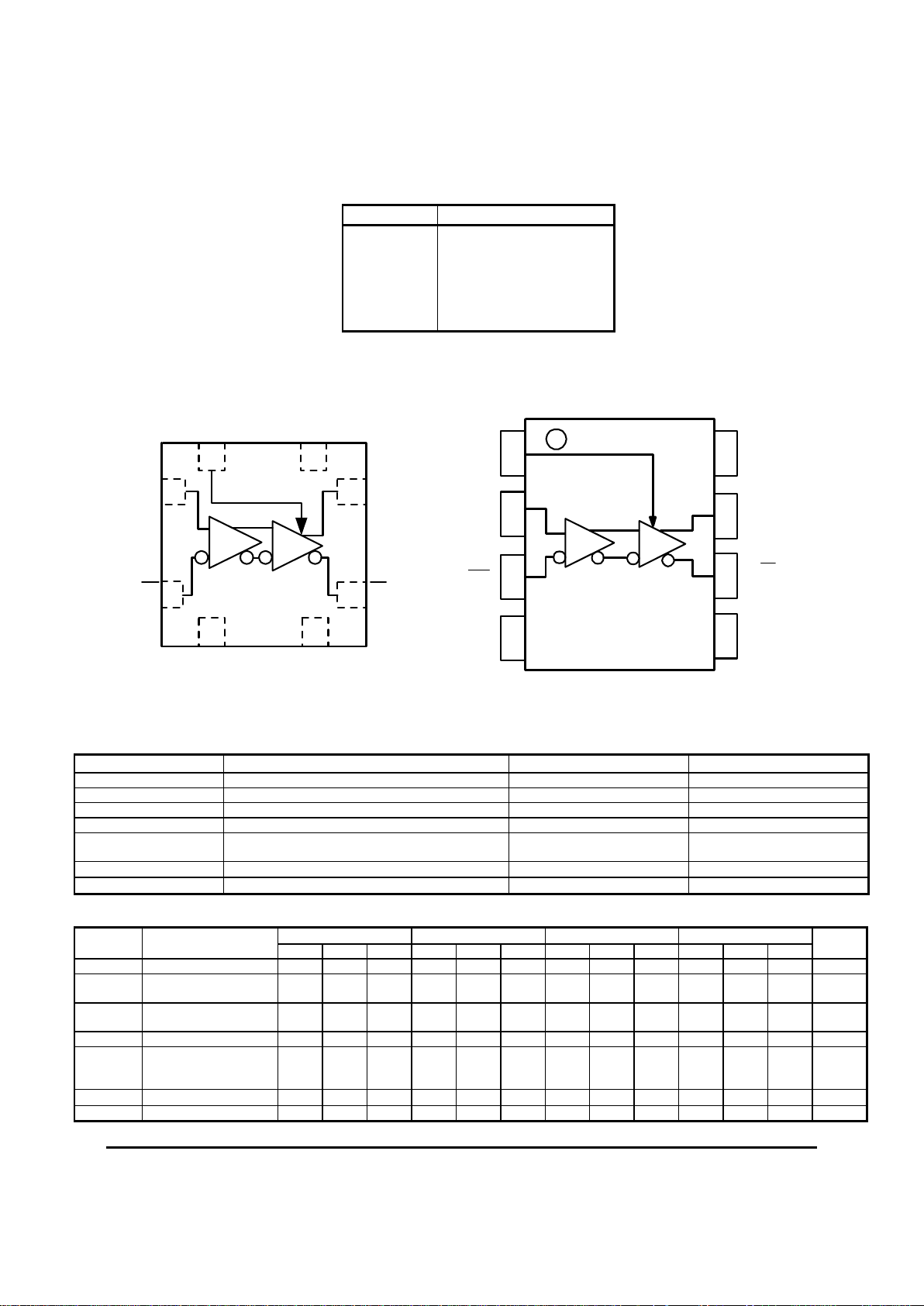
LOGIC DIAGRAM AND PINOUT ASSIGNMENT
PIN DESCRIPTION
PIN FUNCTION
D, D¯ Data Inputs
V
CTRL
Output Swing Control
Q, Q¯ Data Outputs
V
REF
Reference Voltage Output
V
CC
Positive Supply
V
EE
Negative Supply
8
4
5
6
3
2
1
7
V
CC
D
V
EE
Q
Q
V
REF
D
V
CTRL
8 SOIC & 8 TSSOP
MLP 8 (TOP VIEW)
8
5
6
7
4
3
2
1
V
CC
D
V
EE
Q
Q
V
REF
D
V
CTRL
AZ10EP16VS
AZ100EP16VS
November 2001 * REV - 3 www.azmicrotek.com
3
10K LVPECL DC Characteristics (V
EE
= GND, VCC = +3.3V)
-40°C 0°C 25°C 85°C
Symbol Characteristic
Min T
yp
Max Min T
yp
Max Min T
yp
Max Min T
yp
Max
Unit
VOH Output HIGH Voltage
1,2
2215 2465 2280 2405 2530 2340 2590 mV
VOL
Output LOW Voltage
2
V
CTRL
= V
REF
1185 1435 1250 1375 1500 1310 1560 mV
VOL
Output LOW Voltage
2
V
CTRL
= V
CC
1970 2220 2035 2160 2285 2095 2385 mV
V
REF
Reference Voltage 1600 1700 1800 1630 1730 1830 1650 1750 1850 1700 1800 1900 mV
IIH
Input HIGH Current
D,D¯
V
CTRL
80
400
80
400
80
400
80
400
µA
IIL
Input LOW Current 0.5 0.5 0.5 0.5
µA
IEE Power Supply Current 21 27 36 22 28 37 22 29 38 24 30 40 mA
1. For supply voltages other that 3.3V, use the ECL table values and ADD supply voltage value.
2. Each output is terminated through a 50Ω resistor to V
CC
– 2V.
100K ECL DC Characteristics (VEE = -3.0V to -3.6V, VCC = GND)
-40°C 0°C 25°C 85°C
Symbol Characteristic
Min Typ Max Min Typ Max Min Typ Max Min Typ Max
Unit
VOH Output HIGH Voltage1 -1095 -890 -1035 -890 -1035 -965 -890 -1035 -890 mV
VOL
Output LOW Voltage
1
V
CTRL
= V
REF
-1925 -1835 -1965 -1775 -1965 -1870 -1775 -1965 -1775 mV
VOL
Output LOW Voltage
1
V
CTRL
= V
CC
-1180 -1045 -1160 -970 -1160 -1065 -970 -1160 -970 mV
V
REF
Reference Voltage -1650 -1450 -1650 -1450 -1650 -1550 -1450 -1650 -1450 mV
IIH
Input HIGH Current
D,D¯
V
CTRL
80
400
80
400
80
400
80
400
µA
IIL
Input LOW Current 0.5 0.5 0.5 0.5
µA
IEE Power Supply Current 20 26 35 21 27 36 22 28 38 25 31 41 mA
1. Each output is terminated through a 50Ω resistor to V
CC
– 2V.
100K LVPECL DC Characteristics (VEE = GND, VCC = +3.3V)
-40°C 0°C 25°C 85°C
Symbol Characteristic
Min T
yp
Max Min T
yp
Max Min T
yp
Max Min T
yp
Max
Unit
VOH Output HIGH Voltage
1,2
3905 4110 3965 4110 3965 4035 4110 3965 4110 mV
VOL
Output LOW Voltage
2
V
CTRL
= V
REF
3075 3165 3035 3225 3035 3130 3225 3035 3225 mV
VOL
Output LOW Voltage
2
V
CTRL
= V
CC
3820 3955 3840 4030 3840 3935 4030 3840 4030 mV
V
REF
Reference Voltage 1650 1850 1650 1850 1650 1750 1850 1650 1850 mV
IIH
Input HIGH Current
D,D¯
V
CTRL
80
400
80
400
80
400
80
400
µA
IIL
Input LOW Current 0.5 0.5 0.5 0.5
µA
IEE Power Supply Current 20 26 35 21 27 36 22 28 38 25 31 41 mA
1. For supply voltages other that 3.3V, use the ECL table values and ADD supply voltage value.
2. Each output is terminated through a 50Ω resistor to V
CC
– 2V.
 Loading...