

AZMIC AZ10ELT20DR2, AZ10ELT20DR1, AZ10ELT20D, AZ10ELT20X, AZ10ELT20TR2 Datasheet
...
AZ10ELT20
AZ100ELT20
CMOS/TTL to Differential PECL Translator
1630 S. STAPLEY DR., SUITE 125 • MESA, ARIZONA 85204 • USA • (480) 962-5881 • FAX (480) 890-2541
www.azmicrotek.com
ARIZONA MICROTEK, INC.
FEATURES
• 0.5ns Typical Propagation Delay
• Differential PECL Outputs
• Flow Through Pinouts
• Operating Range of +3.0V to +5.5V
• Direct Replacement for ON Semiconductor
MC10ELT20 & MC100ELT20
• Available in a 3x3mm MLP Package
DESCRIPTION
The AZ10/100ELT20 is a CMOS/TTL to differential PECL translator. Because PECL (Positive ECL) levels are
used, only V
CC
and ground are required. The small outline packaging and the single gate of the ELT20 makes it ideal
for those applications where space, performance and low power are at a premium.
The ELT20 is available in both PECL standards: the 10ELT is compatible with PECL 10K logic levels while
the 100ELT is compatible with PECL 100K logic levels.
NOTE: Specifications in PECL tables are valid when thermal equilibrium is established.
BLOCK DIAGRAM
D
Q
Q
PACKAGE AVAILABILITY
PACKAGE PART NO. MARKING
SOIC 8 AZ10ELT20D AZM10ELT20
SOIC 8 T&R AZ10ELT20DR1 AZM10ELT20
SOIC 8 T&R AZ10ELT20DR2 AZM10ELT20
SOIC 8 AZ100ELT20D AZM100ELT20
SOIC 8 T&R AZ100ELT20DR1 AZM100ELT20
SOIC 8 T&R AZ100ELT20DR2 AZM100ELT20
MLP 16 AZ10/100ELT20L AZMT20
MLP 16 T&R AZ10/100ELT20LR1 AZMT20
MLP 16 T&R AZ10/100ELT20LR2 AZMT20
TSSOP 8 AZ10ELT20T AZTLT20
TSSOP 8 T&R AZ10ELT20TR1 AZTLT20
TSSOP 8 T&R AZ10ELT20TR2 AZTLT20
TSSOP 8 AZ100ELT20T AZHLT20
TSSOP 8 T&R AZ100ELT20TR1 AZHLT20
TSSOP 8 T&R AZ100ELT20TR2 AZHLT20
DIE AZ10/100ELT20X N/A
PIN DESCRIPTION
PIN FUNCTION
Q, Q¯ Differential PECL Outputs
D TTL/CMOS Input
GND Ground
VCC Positive Supply
NC No Connect
10K 10K/100K Mode Select
AZ10ELT20
AZ100ELT20
August 2003 * REV - 8 www.azmicrotek.com
2
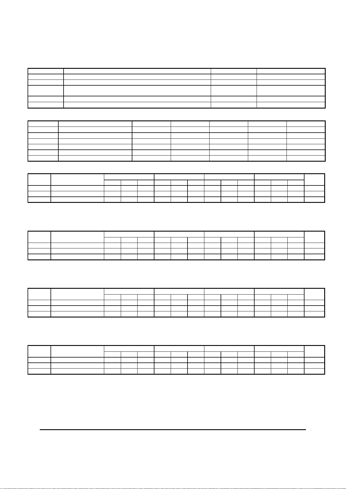
Absolute Maximum Ratings are those values beyond which device life may be impaired.
Symbol Characteristic Value Unit
VCC DC Supply Voltage (Referenced to GND) 0 to +8.0 V
VIN Input Voltage 0 to +6.0 V
I
OUT
Current Applied to Output in Low Output State — Continuous
— Surge
50
100
mA
TA
Operating Temperature Range (In Free-Air) -40 to +85
°C
T
STG
Storage Temperature Range -65 to +150
°C
TTL/CMOS INPUT DC CHARACTERISTICS (GND = 0.0V, VCC = +3.0V to +5.5V)
Symbol Characteristic Min Typ Max Unit Condition
IIH Input HIGH Current 15
µA
VIN = 2.7V
I
IHH
Input HIGH Current 20
µA
VIN = VCC
IIL Input LOW Current -0.1 mA VIN = 0.5V
VIK Input Clamp Diode Voltage -1.2 V IIN = -18mA
VIH Input HIGH Voltage 2.0 V
VIL Input LOW Voltage 0.8 V
10K LVPECL DC Characteristics (GND = 0.0V, VCC = +3.3V)
-40°C 0°C 25°C 85°C
Symbol Characteristic
Min T
yp
Max Min T
yp
Max Min T
yp
Max Min T
yp
Max
Unit
VOH Output HIGH Voltage
1,2
2170 2410 2245 2460 2295 2400 2490 2390 2580 mV
VOL Output LOW Voltage
1,2
1350 1685 1350 1670 1350 1550 1670 1350 1705 mV
ICC Power Supply Current
3
16 16 16 16 mA
1. Output parameters vary 1:1 with VCC.
2. Each output is terminated through a 50Ω resistor to V
CC
– 2V.
3. I
CC
measurements must be done with outputs open.
10K PECL DC Characteristics (GND = 0.0V, VCC = +5.0V)
-40°C 0°C 25°C 85°C
Symbol Characteristic
Min T
yp
Max Min T
yp
Max Min T
yp
Max Min T
yp
Max
Unit
VOH Output HIGH Voltage
1,2
3870 4110 3945 4160 3995 4100 4190 4090 4280 mV
VOL Output LOW Voltage
1,2
3050 3385 3050 3370 3050 3250 3370 3050 3405 mV
ICC Power Supply Current
3
16 16 16 16 mA
1. Output parameters vary 1:1 with VCC.
2. Each output is terminated through a 50Ω resistor to V
CC
– 2V.
3. I
CC
measurements must be done with outputs open.
100K LVPECL DC Characteristics (GND = 0.0V, VCC = +3.3V)
-40°C 0°C 25°C 85°C
Symbol Characteristic
Min T
yp
Max Min T
yp
Max Min T
yp
Max Min T
yp
Max
Unit
VOH Output HIGH Voltage
1,2
2160 2420 2205 2420 2235 2345 2420 2255 2420 mV
VOL Output LOW Voltage
1,2
1400 1745 1400 1680 1400 1595 1680 1400 1680 mV
ICC Power Supply Current
3
16 16 16 16 mA
1. Output parameters vary 1:1 with VCC.
2. Each output is terminated through a 50Ω resistor to V
CC
– 2V.
3. I
CC
measurements must be done with outputs open.
100K PECL DC Characteristics (GND = 0.0V, VCC = +5.0V)
-40°C 0°C 25°C 85°C
Symbol Characteristic
Min T
yp
Max Min T
yp
Max Min T
yp
Max Min T
yp
Max
Unit
VOH Output HIGH Voltage
1,2
3860 4120 3905 4120 3935 4045 4120 3955 4120 mV
VOL Output LOW Voltage
1,2
3100 3445 3100 3380 3100 3295 3380 3100 3380 mV
ICC Power Supply Current
3
16 16 16 16 mA
1. Output parameters vary 1:1 with VCC.
2. Each output is terminated through a 50Ω resistor to V
CC
– 2V.
3. I
CC
measurements must be done with outputs open.
AZ10ELT20
AZ100ELT20
August 2003 * REV - 8 www.azmicrotek.com
3
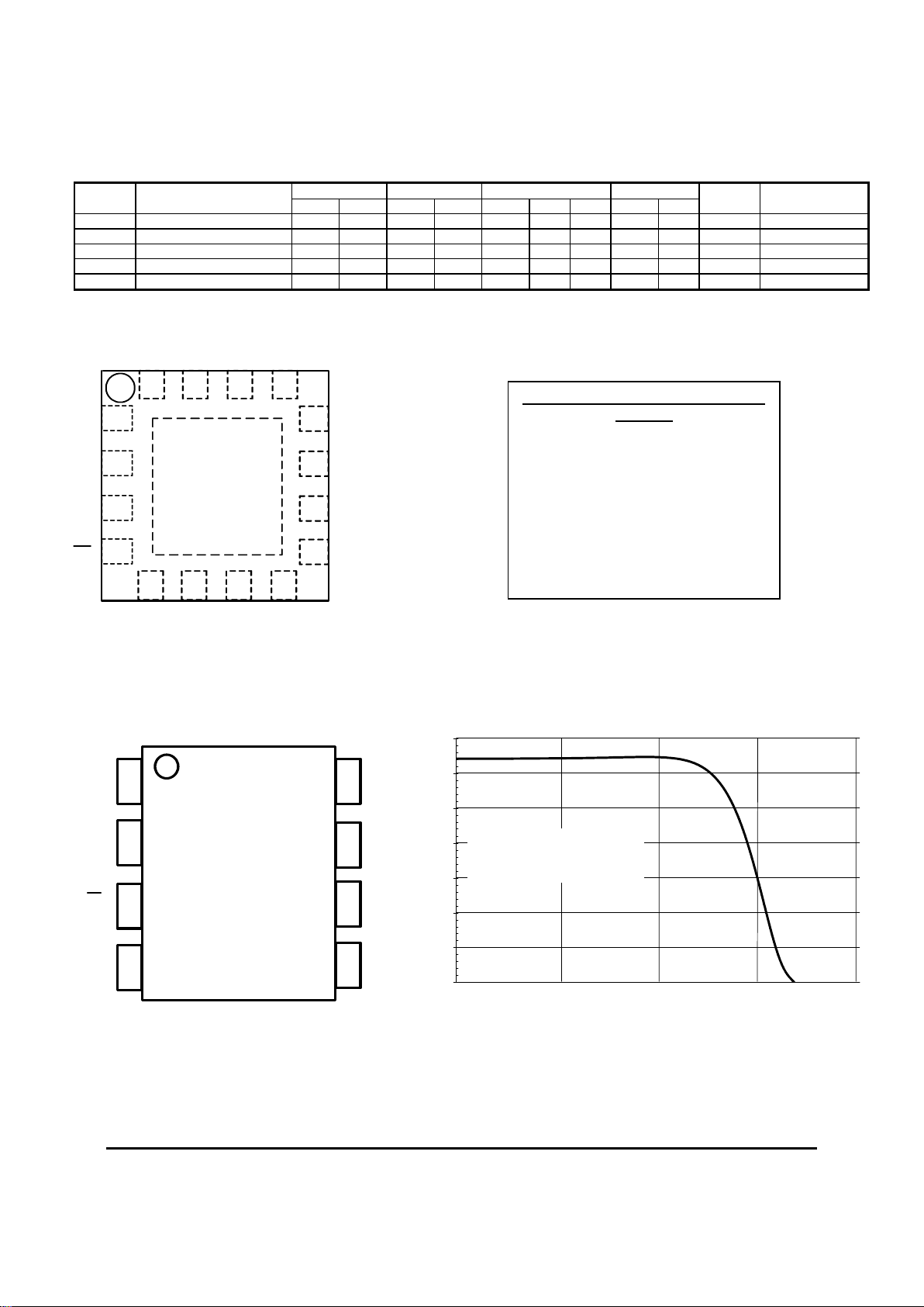
AC CHARACTERISTICS (GND = 0.0V, V
CC
= +3.0V to +5.5V)
-400C
0°C 25°C 85°C
Symbol Characteristic
Min Max Min Max Min Typ Max Min Max
Unit Condition
t
PLH
Propagation Delay1 0.2 0.7 0.2 0.7 0.2 0.4 0.7 0.2 0.7 ns
t
PHL
Propagation Delay1 0.2 0.7 0.2 0.7 0.2 0.4 0.7 0.2 0.7 ns
tr/tf Output Rise/Fall Time 0.25 0.7 0.25 0.7 0.25 0.4 0.7 0.25 0.7 ns 20-80%
f
MAX
Maximum Frequency2 350 350 350 350 MHz
f
MAX
Maximum Frequency3 670 800 800 800 MHz
1. Propagation delay is measured from +1.5V on the input to 50% of the PECL output swing. Input rise/fall times are < 1ns/V.
2. Full swing PECL output.
3. Output at –3 dB.
8
5
6
7
4
3
2
1
V
CC
D
NC
GND
NC
Q
Q
NC
SOIC 8
TSSOP 8
NC
NC
NC
GND
NC
D
4
3
2
1
58
7
6
10
9
12
11
NC
NC
10K
13
14
15
16
V
CC
Q
NC
NC
MLP
16
Q
NC
NC
Large Signal Performance
150
250
350
450
550
650
750
850
1 1 0 100 1000 10000
Frequency (MHz)
Single ended Output (mV p-p)
Input: 150mV p-p Sine
Wave Single Ended
MLP 16 Package and DIE: 10K/100K
Selection
Connect pin/pad 10K to GND to select
10K operation. Float (NC) pin/pad 10K
to select 100K operation. GND
connection must be less than 1Ω.
Pin 8 of the MLP 16 package may be
connected to pin 7 (GND) with no effect
on the circuit.
Top View
 Loading...