

AZMIC AZ10EL89DR2, AZ10EL89DR1, AZ10EL89D Datasheet
ARIZONA MICROTEK, INC.
AZ10EL89
ECL/PECL Coaxial Cable Driver
FEATURES
• 375ps Propagation Delay
• 1.6V Output Swing
• Internal Input Pulldown Resistors
• Operating Range of 4.2V to 5.7V
• Direct Replacement for ON Semiconductor
MC10EL89
• Transistor Count = 29 devices
PACKAGE PART NO. MARKING
SOIC 8 AZ10EL89D AZM10EL89
SOIC 8 T&R AZ10EL89DR1 AZM10EL89
SOIC 8 T&R AZ10EL89DR2 AZM10EL89
DESCRIPTION
The AZ10EL89 is a differential fanout gate specifically designed to drive coaxial cables. The device is
especially useful in Digital Video Broadcasting applications. For this application, since the system is polarity free,
each output can be used as an independent driver. The driver has a voltage gain of approximately 40 and produces
an output swing twice as large as standard ECL output. When driving a coaxial cable, proper termination is required
at both ends of the line to minimize signal loss. The 1.6 V output swing allows for termination at both ends of the
cable, while maintaining the required 800 mV swing at the receiving end of the cable. Because of the larger output
swings, the device cannot be terminated into the standard V
50Ω to V
Broadcast standard -5.0V supply. Under open input conditions (pulled to V
Qn output LOW.
NOTE: Specifications in ECL/PECL tables are valid when thermal equilibrium is established.
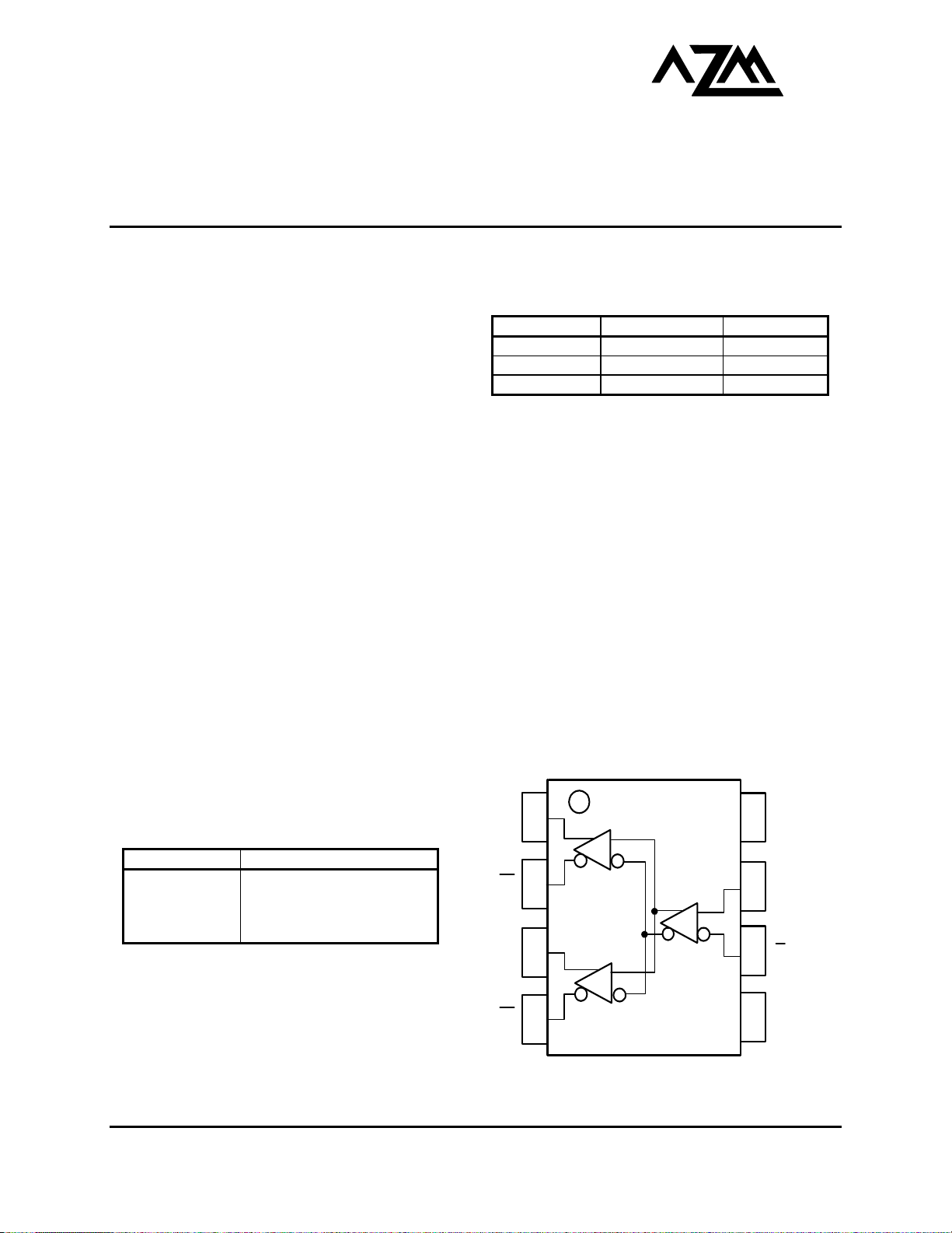
D, D¯ Data Inputs
Q0, Q0¯¯,Q1, Q1¯¯ Data Outputs (1.6VPP)
V
V
1630 S. STAPLEY DR., SUITE 125 • MESA, ARIZONA 85204 • USA • (480) 962-5881 • FAX (480) 890-2541
-3.0V load. The driver accepts a standard differential ECL input and can run off of the Digital Video
CC
CC
EE
PIN DESCRIPTION
PIN FUNCTION
Positive Supply
Negative Supply
www.azmicrotek.com
-2.0V. All of the DC parameters are tested with a
CC
LOGIC DIAGRAM AND PINOUT ASSIGNMENT
Q0
Q0
Q1
Q1
PACKAGE AVAILABILITY
) internal input clamps will force the
EE
1
2
3
4
8
7
6
5
V
CC
D
D
V
EE
AZ10EL89
yp
yp
yp
yp
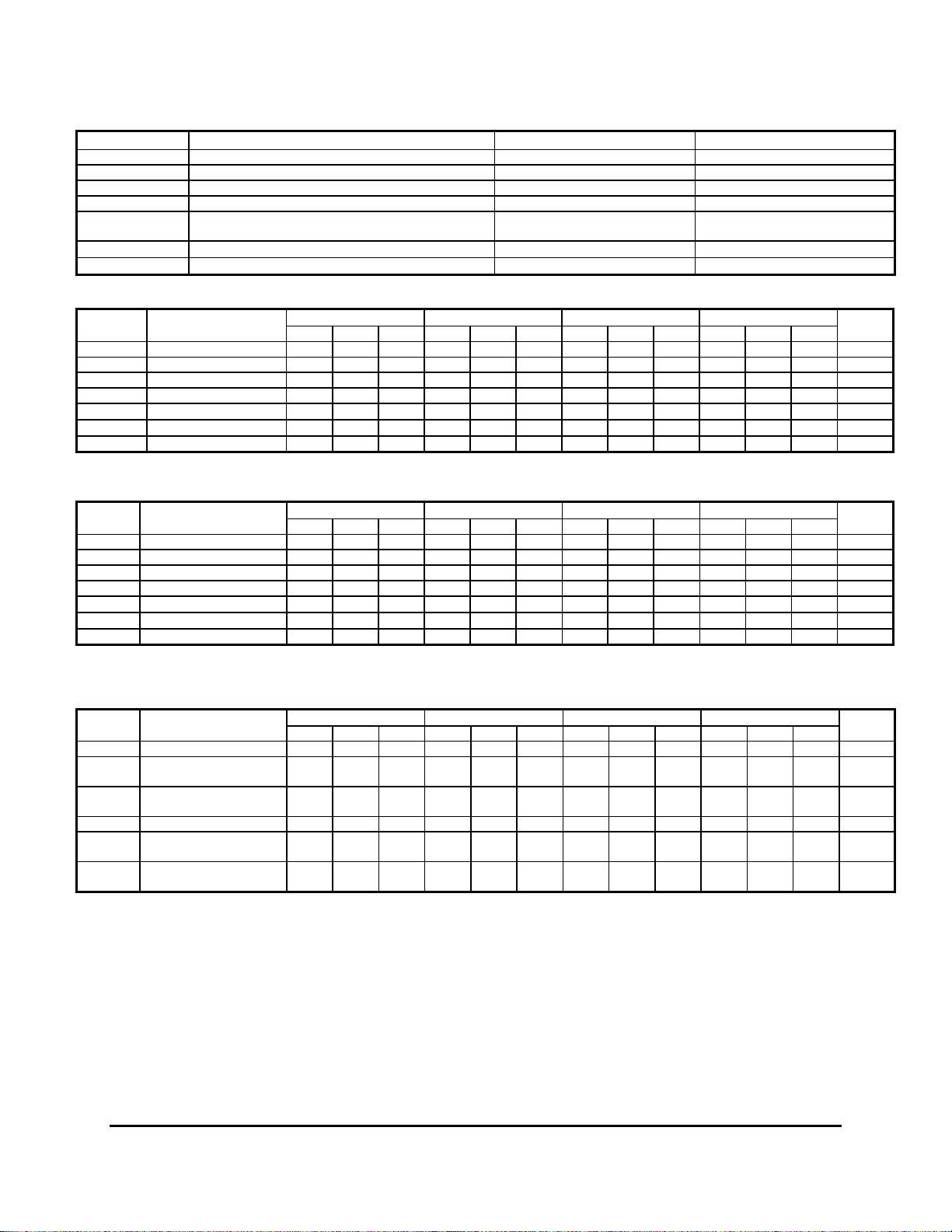
Absolute Maximum Ratings are those values beyond which device life may be impaired.
Symbol Characteristic Rating Unit
VCC PECL Power Supply (VEE = 0V) 0 to +8.0 Vdc
VI PECL Input Voltage (V
= 0V) 0 to +6.0 Vdc
EE
VEE ECL Power Supply (VCC = 0V) -8.0 to 0 Vdc
VI ECL Input Voltage (VCC = 0V) -6.0 to 0 Vdc
I
OUT
Output Current --- Continuous
--- Surge
50
100
TA Operating Temperature Range -40 to +85
T
STG
Storage Temperature Range -65 to +150
10K ECL DC Characteristics (VEE = -4.2V to -5.7V, VCC = GND)
Symbol Characteristic
VOH Output HIGH Voltage1 -1230 -980 -1180 -940 -1130 -900 -1060 -810 mV
VOL Output LOW Voltage1 -2900 -2580 -2950 -2570 -3000 -2560 -3050 -2510 mV
VIH Input HIGH Voltage -1230 -890 -1170 -840 -1130 -810 -1060 -720 mV
VIL Input LOW Voltage -1950 -1500 -1950 -1480 -1950 -1480 -1950 -1445 mV
IIL
IIH
Input LOW Current 0.5
Input HIGH Current 150 150 150 150
IEE Power Supply Current 23 28 23 28 23 28 23 28 mA
1. Each output is terminated through a 50Ω resistor to V
-40°C 0°C 25°C 85°C
Min Typ Max Min Typ Max Min Typ Max Min Typ Max
0.5 0.5 0.5
– 3V.
CC
10K PECL DC Characteristics (VEE = GND, VCC = +5.0V)
Symbol Characteristic
VOH Output HIGH Voltage
VOL Output LOW Voltage
1,2
3770 4020 3820 4060 3870 4100 3940 4190 mV
1,2
2100 2420 2050 2430 2000 2440 1950 2490 mV
VIH Input HIGH Voltage1 3770 4110 3830 4160 3870 4190 3940 4280 mV
VIL Input LOW Voltage1 3050 3500 3050 3520 3050 3520 3050 3555 mV
IIL
Input LOW Current 0.5
IIH Input HIGH Current 150 150 150 150
IEE Power Supply Current 23 28 23 28 23 28 23 28 mA
1. For supply voltages other that 5.0V, use the ECL table values and ADD supply voltage value.
2. Each output is terminated through a 50Ω resistor to V
-40°C 0°C 25°C 85°C
Min T
Max Min T
Max Min T
0.5 0.5 0.5
– 3V.
CC
AC Characteristics (VEE = -4.2V to -5.7V, VCC = GND or VEE = GND, VCC = +4.2V to +5.7V)
Symbol Characteristic
t
max
t
PLH / tPHL
t
SKEW
V
PP
V
CMR
tr / tf
Maximum Toggle Rate 1.5 Gb/s
Propagation Delay
to Output
Within-Device Skew
Duty Cycle Skew
(AC) Minimum Input Swing
Common Mode Range
1
2
3
4
Output Rise/Fall Times Q
(20% - 80%)
1. Within-device skew defined as identical transitions on similar paths through a device.
2. Duty cycle skew is the difference between a t
is the minimum peak-to-peak differential input swing for which AC parameters guaranteed. The device has a DC gain of ≈ 40.
3. V
PP
4. The V
range is referenced to the most positive side of the differential input signal. Normal operation is obtained if the HIGH level falls within
CMR
the specified range and the peak-to-peak voltage lies between V
-40°C 0°C 25°C 85°C
Min Typ Max Min Typ Max Min Typ Max Min Typ Max
200 340 480 250 340 430 260 350 440 310 400 490 ps
5 20 5 20 5 20 5 20 ps
150 150 150 150 mV
VEE +
2.5
V
CC
0.4
-
VEE +
2.5
V
CC
0.4
-
VEE +
2.5
205 455 205 455 205 455 205 455 ps
and t
PLH
propagation delay through a device.
PHL
(min) and 1V.
PP
Max Min T
-
V
CC
0.4
VEE +
2.5
mA
°C
°C
Unit
µA
µA
Max
Unit
µA
µA
Unit
-
V
CC
0.4
V
October 2001 * REV - 0 www.azmicrotek.com
2
 Loading...