

AZMIC AZ10EL57DR2, AZ10EL57DR1, AZ10EL57D, AZ100EL57DR2, AZ100EL57DR1 Datasheet
...
AZ10EL57
AZ100EL57
ECL/PECL 4:1 Differential Multiplexer
1630 S. STAPLEY DR., SUITE 125 • MESA, ARIZONA 85204 • USA • (480) 962-5881 • FAX (480) 890-2541
www.azmicrotek.com
ARIZONA MICROTEK, INC.
FEATURES
• 75kΩ Internal Input Pulldown Resistors
• 2:1 Operation When SEL1 Not Connected
• Multiple V
BB
Outputs Allow Single-ended
Operation
• Direct Replacement for ON Semiconductor
MC10EL57 & MC100EL57
DESCRIPTION
The AZ10/100EL57 is a fully differential 4:1 multiplexer. By leaving the SEL1 line open (pulled LOW via the
input pulldown resistor) the device can also be used as a differential 2:1 multiplexer with the SEL0 input selecting
between D0 and D1. The fully differential architecture of the EL57 makes it ideal for use in low skew applications
such as clock distribution.
SEL1 is the most significant select line. The binary number applied to the select inputs will select the same
numbered data input (i.e., 00 selects D0, 01 selects D1, etc.).
The EL57 provides two V
BB
outputs for single-ended use or a DC bias reference for AC coupling to the device.
For single-ended input applications, the V
BB
reference should be connected to one side of the Dn/D¯n differential
input pair. The input signal is then fed to the other Dn/D¯n input. The V
BB
pins should be used only as a bias for the
EL57 as its current sink/source capability is limited. When used, the V
BB
pins should be bypassed to ground via a
0.01µF capacitor.
NOTE: Specifications in the ECL/PECL tables are valid when thermal equilibrium is established.
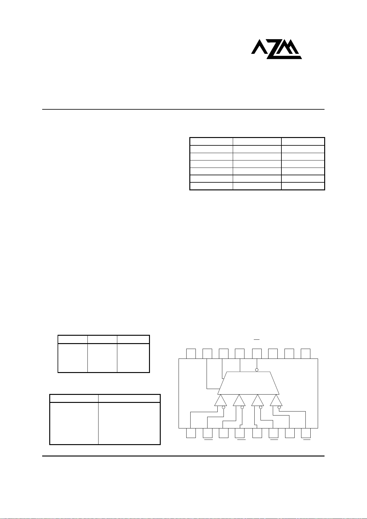
PACKAGE AVAILABILITY
PACKAGE PART NO. MARKING
SOIC 16 AZ10EL57D AZM10EL57
SOIC 16 T&R AZ10EL57DR1 AZM10EL57
SOIC 16 T&R AZ10EL57DR2 AZM10EL57
SOIC 16 AZ100EL57D AZM100EL57
SOIC 16 T&R AZ100EL57DR1 AZM100EL57
SOIC 16 T&R AZ100EL57DR2 AZM100EL57
FUNCTION TABLE
SEL1 SEL0 Q
L L D0
L H D1
H L D2
H H D3
PIN DESCRIPTION
PIN FUNCTION
D0, D0¯¯ – D3, D3¯¯ Data Input Pairs
SEL0, SEL1 Mux Select Inputs
V
BB1, VBB2
Reference Outputs
Q, Q¯ Data Outputs
V
CC
Positive Supply
V
EE
Negative Supply
LOGIC DIAGRAM AND PINOUT ASSIGNMENT
SEL0
SEL1
QQ
D0 D0 D1 D1 D2 D3 D3D2
V
CC
V
BB1VBB2VEE
16 15 14 13 12 11 10 9
87654321
4:1
AZ10EL57
AZ100EL57
October 2001 * REV - 2 www.azmicrotek.com
2
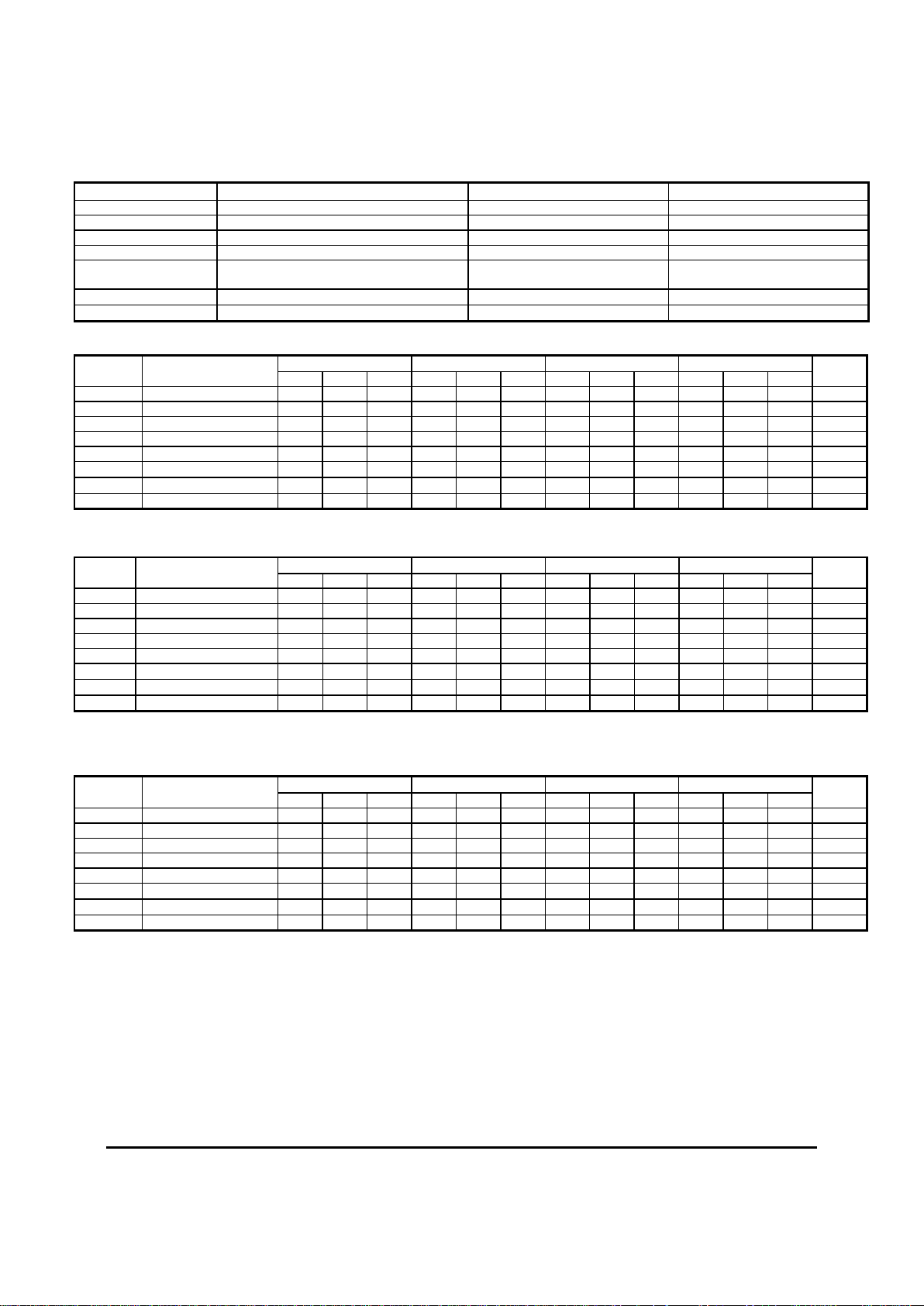
Absolute Maximum Ratings are those values beyond which device life may be impaired.
Symbol Characteristic Rating Unit
VCC PECL Power Supply (VEE = 0V) 0 to +8.0 Vdc
VI PECL Input Voltage (V
EE
= 0V) 0 to +6.0 Vdc
VEE ECL Power Supply (VCC = 0V) -8.0 to 0 Vdc
VI ECL Input Voltage (VCC = 0V) -6.0 to 0 Vdc
I
OUT
Output Current --- Continuous
--- Surge
50
100
mA
TA Operating Temperature Range -40 to +85
°C
T
STG
Storage Temperature Range -65 to +150
°C
10K ECL DC Characteristics (VEE = -4.75V to -5.5V, VCC = GND)
-40°C 0°C 25°C 85°C
Symbol Characteristic
Min Typ Max Min Typ Max Min Typ Max Min Typ Max
Unit
VOH Output HIGH Voltage1 -1080 -890 -1020 -840 -980 -810 -910 -720 mV
VOL Output LOW Voltage1 -1950 -1650 -1950 -1630 -1950 -1630 -1950 -1595 mV
VIH Input HIGH Voltage -1230 -890 -1170 -840 -1130 -810 -1060 -720 mV
VIL Input LOW Voltage -1950 -1500 -1950 -1480 -1950 -1480 -1950 -1445 mV
VBB Reference Voltage -1430 -1300 -1380 -1270 -1350 -1250 -1310 -1190 mV
IIH
Input HIGH Current 150 150 150 150
µA
IIL
Input LOW Current 0.5 0.5 0.5 0.5
µA
IEE Power Supply Current 24 24 24 24 mA
1. Each output is terminated through a 50Ω resistor to V
CC
– 2V.
10K PECL DC Characteristics (VEE = GND, VCC = +5.0V)
-40°C 0°C 25°C 85°C
Symbol Characteristic
Min T
yp
Max Min T
yp
Max Min T
yp
Max Min T
yp
Max
Unit
VOH Output HIGH Voltage
1,2
3920 4110 3980 4160 4020 4190 4090 4280 mV
VOL Output LOW Voltage
1,2
3050 3350 3050 3370 3050 3370 3050 3405 mV
VIH Input HIGH Voltage1 3770 4110 3830 4160 3870 4190 3940 4280 mV
VIL Input LOW Voltage1 3050 3500 3050 3520 3050 3520 3050 3555 mV
VBB Reference Voltage1 3570 3700 3620 3730 3650 3750 3690 3810 mV
IIH Input HIGH Current 150 150 150 150
µA
IIL
Input LOW Current 0.5 0.5 0.5 0.5
µA
IEE Power Supply Current 24 24 24 24 mA
1. For supply voltages other that 5.0V, use the ECL table values and ADD supply voltage value.
2. Each output is terminated through a 50Ω resistor to V
CC
– 2V.
100K ECL DC Characteristics (V
EE
= -4.2V to -5.5V, VCC = GND)
-40°C 0°C 25°C 85°C
Symbol Characteristic
Min Typ Max Min Typ Max Min Typ Max Min Typ Max
Unit
VOH Output HIGH Voltage1 -1085 -1005 -880 -1025 -955 -880 -1025 -955 -880 -1025 -955 -880 mV
VOL Output LOW Voltage1 -1830 -1695 -1555 -1810 -1705 -1620 -1810 -1705 -1620 -1810 -1705 -1620 mV
VIH Input HIGH Voltage -1165 -880 -1165 -880 -1165 -880 -1165 -880 mV
VIL Input LOW Voltage -1810 -1475 -1810 -1475 -1810 -1475 -1810 -1475 mV
VBB Reference Voltage -1380 -1260 -1380 -1260 -1380 -1260 -1380 -1260 mV
IIH
Input HIGH Current 150 150 150 150
µA
IIL
Input LOW Current 0.5 0.5 0.5 0.5
µA
IEE Power Supply Current 24 24 24 27 mA
1. Each output is terminated through a 50Ω resistor to V
CC
– 2V.
 Loading...