

AZMIC AZ10EL31TR2, AZ10EL31TR1, AZ10EL31T, AZ10EL31DR2, AZ10EL31DR1 Datasheet
...
ARIZONA MICROTEK, INC.
AZ10EL31
AZ100EL31
ECL/PECL D Flip-Flop with Set and Reset
FEATURES
• 475ps Propagation Delay
• 2.8GHz Toggle Frequency
• 75kΩ Internal Input Pulldown Resistors
• Direct Replacement for ON Semiconductor
MC10EL31 & MC100EL31
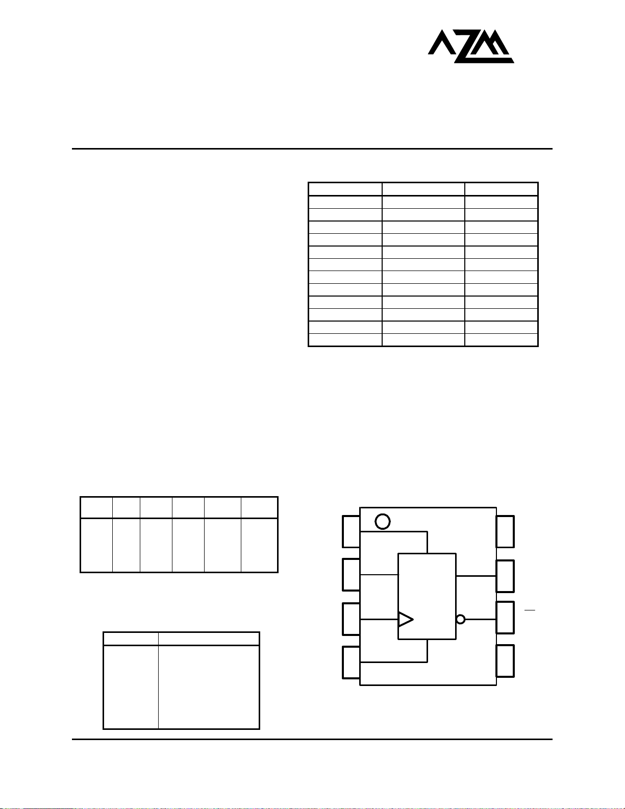
PACKAGE PART NO. MARKING
SOIC 8 AZ10EL31D AZM10EL31
SOIC 8 T&R AZ10EL31DR1 AZM10EL31
SOIC 8 T&R AZ10EL31DR2 AZM10EL31
SOIC 8 AZ100EL31D AZM100EL31
SOIC 8 T&R AZ100EL31DR1 AZM100EL31
SOIC 8 T&R AZ100EL31DR2 AZM100EL31
TSSOP 8 AZ10EL31T AZTEL31
TSSOP 8 T&R AZ10EL31TR1 AZTEL31
TSSOP 8 T&R AZ10EL31TR2 AZTEL31
TSSOP 8 AZ100EL31T AZHEL31
TSSOP 8 T&R AZ100EL31TR1 AZHEL31
TSSOP 8 T&R AZ100EL31TR2 AZHEL31
PACKAGE AVAILABILITY
DESCRIPTION
The AZ10/100EL31 is a master-slave D flip-flop with set and reset. The device is functionally equivalent to the
E131 device with higher performance capabilities. With propagation delays and output transition times significantly
faster than the E131, the EL31 is ideally suited for those applications that require the ultimate in AC performance.
Both set and reset inputs are asynchronous, level triggered signals. Data enters the master section of the flipflop when the clock is LOW. When the clock transitions from LOW to HIGH, the data in the master section
transfers into the slave section and through to the outputs.
NOTE: Specifications in ECL/PECL tables are valid when thermal equilibrium is established.
D
L L L Z L H
H L L Z H L
X H L X H L
X L H X L H
X H H X Undef Undef
* Pins will default low when left open
S Set Input
D Data Input
R Reset Input
CLK Clock Input
Q, Q¯ Data Outputs
VCC Positive Supply
VEE Negative Supply
1630 S. STAPLEY DR., SUITE 125 • MESA, ARIZONA 85204 • USA • (480) 962-5881 • FAX (480) 890-2541
TRUTH TABLE
S* R* CLK Q
Z = LOW to HIGH Transition
PIN DESCRIPTION
PIN FUNCTION
Q¯
www.azmicrotek.com
LOGIC DIAGRAM AND PINOUT ASSIGNMENT
S
D
CLK
R
1
2
3
4
S
D
Flip Flop
R
8
7
6
5
V
CC
Q
Q
V
EE
AZ10EL31
yp
yp
yp
yp
AZ100EL31
Absolute Maximum Ratings are those values beyond which device life may be impaired.
Symbol Characteristic Rating Unit
VCC PECL Power Supply (VEE = 0V) 0 to +8.0 Vdc
VI PECL Input Voltage (V
VEE ECL Power Supply (VCC = 0V) -8.0 to 0 Vdc
VI ECL Input Voltage (VCC = 0V) -6.0 to 0 Vdc
I
OUT
TA Operating Temperature Range -40 to +85
T
STG
Output Current --- Continuous
--- Surge
Storage Temperature Range -65 to +150
= 0V) 0 to +6.0 Vdc
EE
50
100
10K ECL DC Characteristics (VEE = -4.75 to -5.5V, VCC = GND)
Symbol Characteristic
VOH Output HIGH Voltage1 -1080 -890 -1020 -840 -980 -810 -910 -720 mV
VOL Output LOW Voltage1 -1950 -1650 -1950 -1630 -1950 -1630 -1950 -1595 mV
VIH Input HIGH Voltage -1230 -890 -1170 -840 -1130 -810 -1060 -720 mV
VIL Input LOW Voltage -1950 -1500 -1950 -1480 -1950 -1480 -1950 -1445 mV
IIH
IIL
IEE Power Supply Current 27 32 27 32 27 32 27 32 mA
1. Each output is terminated through a 50Ω resistor to V
Input HIGH Current
D, CLK
S, R
Input LOW Current 0.5 0.5 0.5 0.5
-40°C 0°C 25°C 85°C
Min Typ Max Min Typ Max Min Typ Max Min Typ Max
CC
150
300
– 2V.
150
300
10K PECL DC Characteristics (VEE = GND, VCC = +5.0V)
Symbol Characteristic
VOH Output HIGH Voltage
VOL Output LOW Voltage
VIH Input HIGH Voltage1 3770 4110 3830 4160 3870 4190 3940 4280 mV
VIL Input LOW Voltage1 3050 3500 3050 3520 3050 3520 3050 3555 mV
IIH
IIH Input HIGH Current 150 150 150 150
IIL
IEE Power Supply Current 27 32 27 32 27 32 27 32 mA
1. For supply voltages other that 5.0V, use the ECL table values and ADD supply voltage value.
2. Each output is terminated through a 50Ω resistor to V
Input HIGH Current
Input LOW Current 0.5 0.5 0.5 0.5
1,2
3920 4110 3980 4160 4020 4190 4090 4280 mV
1,2
3050 3350 3050 3370 3050 3370 3050 3405 mV
D, CLK
S, R
-40°C 0°C 25°C 85°C
Min T
Max Min T
CC
150
300
– 2V.
Max Min T
150
300
100K ECL DC Characteristics (V
Symbol Characteristic
VOH Output HIGH Voltage1 -1085 -1005 -880 -1025 -955 -880 -1025 -955 -880 -1025 -955 -880 mV
VOL Output LOW Voltage1 -1830 -1695 -1555 -1810 -1705 -1620 -1810 -1705 -1620 -1810 -1705 -1620 mV
VIH Input HIGH Voltage -1165 -880 -1165 -880 -1165 -880 -1165 -880 mV
VIL Input LOW Voltage -1810 -1475 -1810 -1475 -1810 -1475 -1810 -1475 mV
IIH
IIH
IIL
IEE Power Supply Current 27 32 27 32 27 32 31 37 mA
1. Each output is terminated through a 50Ω resistor to V
Input HIGH Current
D, CLK
S, R
Input HIGH Current 150 150 150 150
Input LOW Current 0.5 0.5 0.5 0.5
= -4.2V to -5.5V, VCC = GND)
EE
-40°C 0°C 25°C 85°C
Min Typ Max Min Typ Max Min Typ Max Min Typ Max
CC
150
300
– 2V.
150
300
150
300
Max Min T
150
300
150
300
mA
°C
°C
150
300
Max
150
300
150
300
Unit
µA
µA
Unit
µA
µA
µA
Unit
µA
µA
µA
October 2001 * REV - 2 www.azmicrotek.com
2
 Loading...