

AZMIC AZ10LVEL16TR2, AZ10LVEL16TR1, AZ10LVEL16T, AZ10LVEL16DR2, AZ10LVEL16DR1 Datasheet
...
AZ10LVEL16
AZ100LVEL16
ECL/PECL Differential Receiver
1630 S. STAPLEY DR., SUITE 125 • MESA, ARIZONA 85204 • USA • (480) 962-5881 • FAX (480) 890-2541
www.azmicrotek.com
ARIZONA MICROTEK, INC.
FEATURES
• 250ps Propagation Delay
• High Bandwidth Output Transitions
• Operating Range of 3.0V to 5.5V
• Internal Input Pulldown Resistors
• Direct Replacement For ON Semiconductor
MC10EL16, MC100EL16, & MC100LVEL16
DESCRIPTION
The AZ10/100LVEL16 is a differential receiver. The device is functionally equivalent to the E116 device with
higher performance capabilities. With output transition times significantly faster than the E116, the LVEL16 is
ideally suited for interfacing with high frequency sources.
The LVEL16 provides a V
BB
output for single-ended use or a DC bias reference for AC coupling to the
device. For single-ended input applications, the V
BB
reference should be connected to one side of the D/D¯
differential input pair. The input signal is then fed to the other D/D¯ input. The V
BB
pin can support 1.5mA
sink/source current. When used, the V
BB
pin should be bypassed to ground via a 0.01µF capacitor.
Under open input conditions internal input clamps will force the Q output LOW.
NOTE: Specifications in the ECL/PECL tables are valid when thermal equilibrium is established.
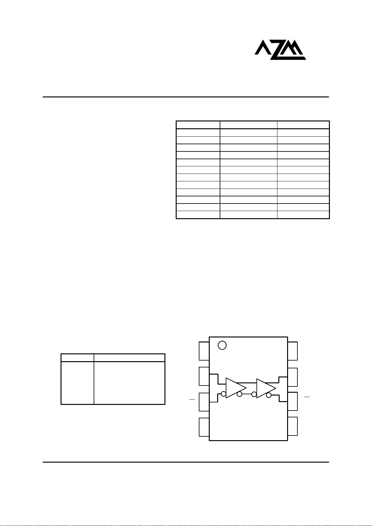
LOGIC DIAGRAM AND PINOUT ASSIGNMENT
8
5
6
7
4
3
2
1
V
CC
D
V
EE
NC
Q
Q
V
BB
D
PACKAGE AVAILABILITY
PACKAGE PART NO. MARKING
SOIC 8 AZ10LVEL16D AZM10LVEL16
SOIC 8 T&R AZ10LVEL16DR1 AZM10LVEL16
SOIC 8 T&R AZ10LVEL16DR2 AZM10LVEL16
SOIC 8 AZ100LVEL16D AZM100LVEL16
SOIC 8 T&R AZ100LVEL16DR1 AZM100LVEL16
SOIC 8 T&R AZ100LVEL16DR2 AZM100LVEL16
TSSOP 8 AZ10LVEL16T AZTLV16
TSSOP 8 T&R AZ10LVEL16TR1 AZTLV16
TSSOP 8 T&R AZ10LVEL16TR2 AZTLV16
TSSOP 8 AZ100LVEL16T AZHLV16
TSSOP 8 T&R AZ100LVEL16TR1 AZHLV16
TSSOP 8 T&R AZ100LVEL16TR2 AZHLV16
PIN DESCRIPTION
PIN FUNCTION
D, D¯ Data Inputs
Q, Q¯ Data Outputs
VBB Reference Voltage Output
V
CC
Positive Supply
V
EE
Negative Supply
NC No Connect
AZ10LVEL16
AZ100LVEL16
October 2001 * REV - 0 www.azmicrotek.com
2
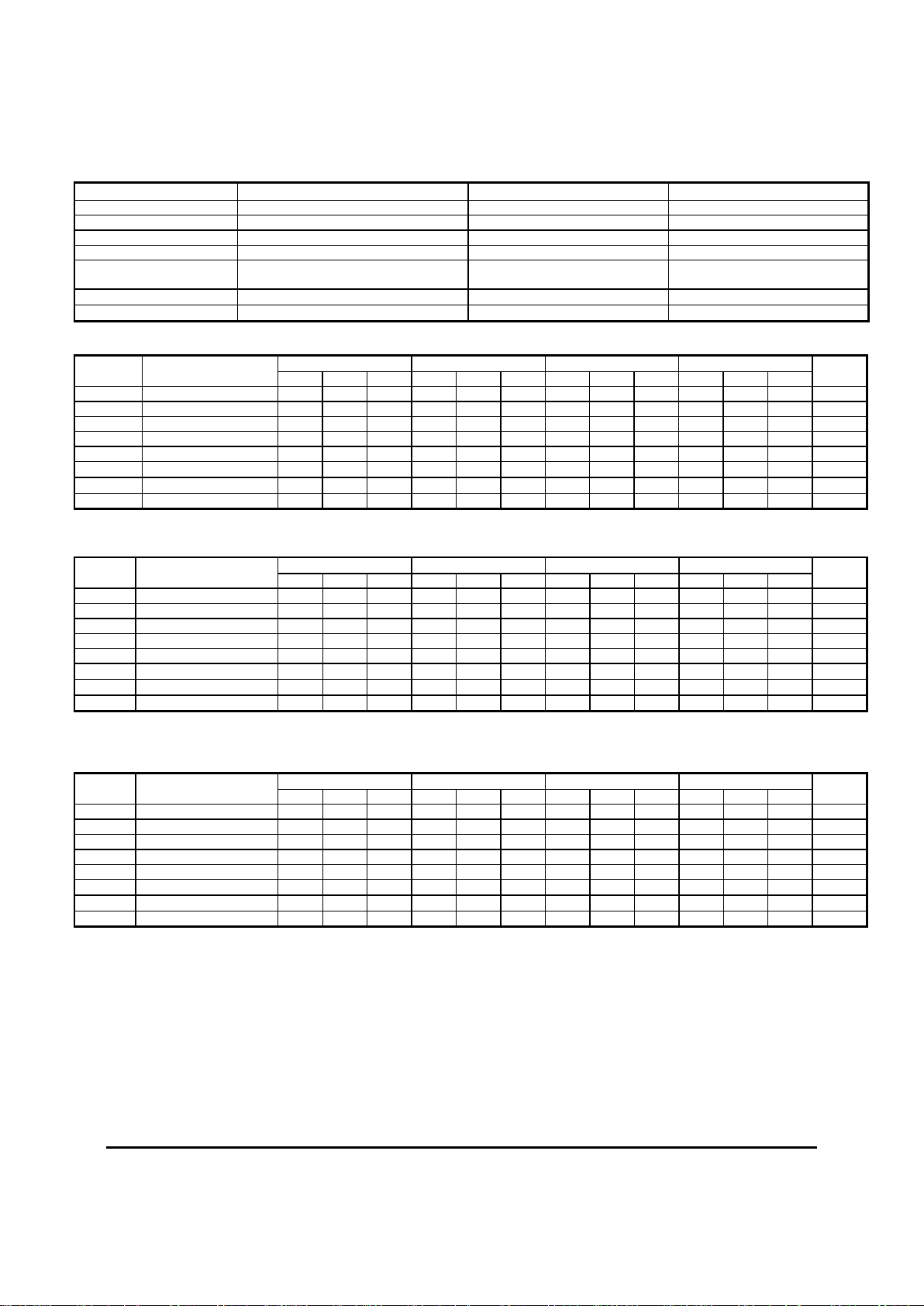
Absolute Maximum Ratings are those values beyond which device life may be impaired.
Symbol Characteristic Rating Unit
VCC PECL Power Supply (VEE = 0V) 0 to +8.0 Vdc
VI PECL Input Voltage (V
EE
= 0V) 0 to +6.0 Vdc
VEE ECL Power Supply (VCC = 0V) -8.0 to 0 Vdc
VI ECL Input Voltage (VCC = 0V) -6.0 to 0 Vdc
I
OUT
Output Current --- Continuous
--- Surge
50
100
mA
TA Operating Temperature Range -40 to +85
°C
T
STG
Storage Temperature Range -65 to +150
°C
10K ECL DC Characteristics (VEE = -3.0V to -5.5V, VCC = GND)
-40°C 0°C 25°C 85°C
Symbol Characteristic
Min Typ Max Min Typ Max Min Typ Max Min Typ Max
Unit
VOH Output HIGH Voltage1 -1080 -890 -1020 -840 -980 -810 -910 -720 mV
VOL Output LOW Voltage1 -1950 -1650 -1950 -1630 -1950 -1630 -1950 -1595 mV
VIH Input HIGH Voltage -1230 -890 -1170 -840 -1130 -810 -1060 -720 mV
VIL Input LOW Voltage -1950 -1500 -1950 -1480 -1950 -1480 -1950 -1445 mV
VBB Reference Voltage -1430 -1300 -1380 -1270 -1350 -1250 -1310 -1190 mV
IIL
Input LOW Current -150 -150 -150 -150
µA
IIH
Input HIGH Current 150 150 150 150
µA
IEE Power Supply Current 18 22 18 22 18 22 18 22 mA
1. Each output is terminated through a 50Ω resistor to V
CC
– 2V.
10K LVPECL DC Characteristics (VEE = GND, VCC = +3.3V)
-40°C 0°C 25°C 85°C
Symbol Characteristic
Min T
yp
Max Min T
yp
Max Min T
yp
Max Min T
yp
Max
Unit
VOH Output HIGH Voltage
1,2
2220 2410 2280 2460 2320 2490 2390 2580 mV
VOL Output LOW Voltage
1,2
1350 1650 1350 1670 1350 1670 1350 1705 mV
VIH Input HIGH Voltage1 2070 2410 2130 2460 2170 2490 2240 2580 mV
VIL Input LOW Voltage1 1350 1800 1350 1820 1350 1820 1350 1855 mV
VBB Reference Voltage1 1870 2000 1920 2030 1950 3050 1990 1390 mV
IIL
Input LOW Current -150 -150 -150 -150
µA
IIH Input HIGH Current 150 150 150 150
µA
IEE Power Supply Current 18 22 18 22 18 22 18 22 mA
1. For supply voltages other that 3.3V, use the ECL table values and ADD supply voltage value.
2. Each output is terminated through a 50Ω resistor to V
CC
– 2V.
10K PECL DC Characteristics (VEE = GND, VCC = +5.0V)
-40°C 0°C 25°C 85°C
Symbol Characteristic
Min T
yp
Max Min T
yp
Max Min T
yp
Max Min T
yp
Max
Unit
VOH Output HIGH Voltage
1,2
3920 4110 3980 4160 4020 4190 4090 4280 mV
VOL Output LOW Voltage
1,2
3050 3350 3050 3370 3050 3370 3050 3405 mV
VIH Input HIGH Voltage1 3770 4110 3830 4160 3870 4190 3940 4280 mV
VIL Input LOW Voltage1 3050 3500 3050 3520 3050 3520 3050 3555 mV
VBB Reference Voltage1 3570 3700 3620 3730 3650 3750 3690 3810 mV
IIL
Input LOW Current -150 -150 -150 -150
µA
IIH Input HIGH Current 150 150 150 150
µA
IEE Power Supply Current 18 22 18 22 18 22 18 22 mA
1. For supply voltages other that 5.0V, use the ECL table values and ADD supply voltage value.
2. Each output is terminated through a 50Ω resistor to V
CC
– 2V.
 Loading...