

AZMIC AZ10LVEL11TR2, AZ10LVEL11TR1, AZ10LVEL11T, AZ10LVEL11DR2, AZ10LVEL11DR1 Datasheet
...
AZ10LVEL11
AZ100LVEL11
ECL/PECL 1:2 Differential Fanout Buffer
1630 S. STAPLEY DR., SUITE 125 • MESA, ARIZONA 85204 • USA • (480) 962-5881 • FAX (480) 890-2541
www.azmicrotek.com
ARIZONA MICROTEK, INC.
FEATURES
• 265ps Propagation Delay
• 5ps Skew Between Outputs
• High Bandwidth Output Transitions
• Internal Input Pulldown Resistors
• Operating Range of 3.0V to 5.5V
• Direct Replacement for ON Semiconductor
MC100LVEL11, MC10EL11 & MC100EL11
• Transistor Count = 51
DESCRIPTION
The AZ10/100LVEL11 is a differential 1:2 fanout gate. The device is functionally similar to the E111 device
but with higher performance capabilities. Having within-device skews and output transition times significantly
improved over the E111, the AZ10/100LVEL11 is ideally suited for those applications that require the ultimate in
AC performance.
The differential inputs of the AZ10/100LVEL11 employ clamping circuitry to maintain stability under open
input conditions. If the inputs are left open, the Q outputs will go LOW.
NOTE: Specifications in the ECL/PECL tables are valid when thermal equilibrium is established.
LOGIC DIAGRAM AND PINOUT ASSIGNMENT
PACKAGE AVAILABILITY
PACKAGE PART NO. MARKING
SOIC 8 AZ10LVEL11D AZM10LVEL11
SOIC 8 T&R AZ10LVEL11DR1 AZM10LVEL11
SOIC 8 T&R AZ10LVEL11DR2 AZM10LVEL11
SOIC 8 AZ100LVEL11D AZM100LVEL11
SOIC 8 T&R AZ100LVEL11DR1 AZM100LVEL11
SOIC 8 T&R AZ100LVEL11DR2 AZM100LVEL11
TSSOP 8 AZ10LVEL11T AZTLV11
TSSOP 8 T&R AZ10LVEL11TR1 AZTLV11
TSSOP 8 T&R AZ10LVEL11TR2 AZTLV11
TSSOP 8 AZ100LVEL11T AZHLV11
TSSOP 8 T&R AZ100LVEL11TR1 AZHLV11
TSSOP 8 T&R AZ100LVEL11TR2 AZHLV11
PIN DESCRIPTION
PIN FUNCTION
D, D¯ Data Inputs
Q0, Q0¯¯,Q1, Q1¯¯ Data Outputs
VCC Positive Supply
VEE Negative Supply
8
5
6
7
4
3
2
1
D
Q0
Q0
Q1
Q1
D
V
CC
V
EE
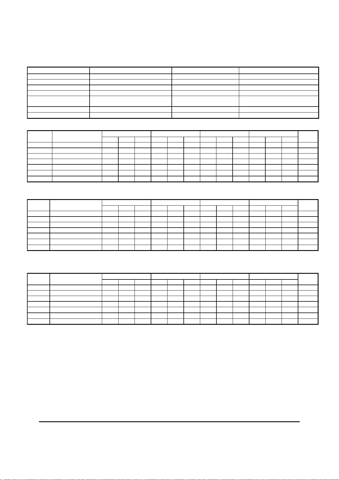
AZ10LVEL11
AZ100LVEL11
October 2001 * REV - 0 www.azmicrotek.com
2
Absolute Maximum Ratings are those values beyond which device life may be impaired.
Symbol Characteristic Rating Unit
VCC PECL Power Supply (VEE = 0V) 0 to +8.0 Vdc
VI PECL Input Voltage (V
EE
= 0V) 0 to +6.0 Vdc
VEE ECL Power Supply (VCC = 0V) -8.0 to 0 Vdc
VI ECL Input Voltage (VCC = 0V) -6.0 to 0 Vdc
I
OUT
Output Current --- Continuous
--- Surge
50
100
mA
TA Operating Temperature Range -40 to +85
°C
T
STG
Storage Temperature Range -65 to +150
°C
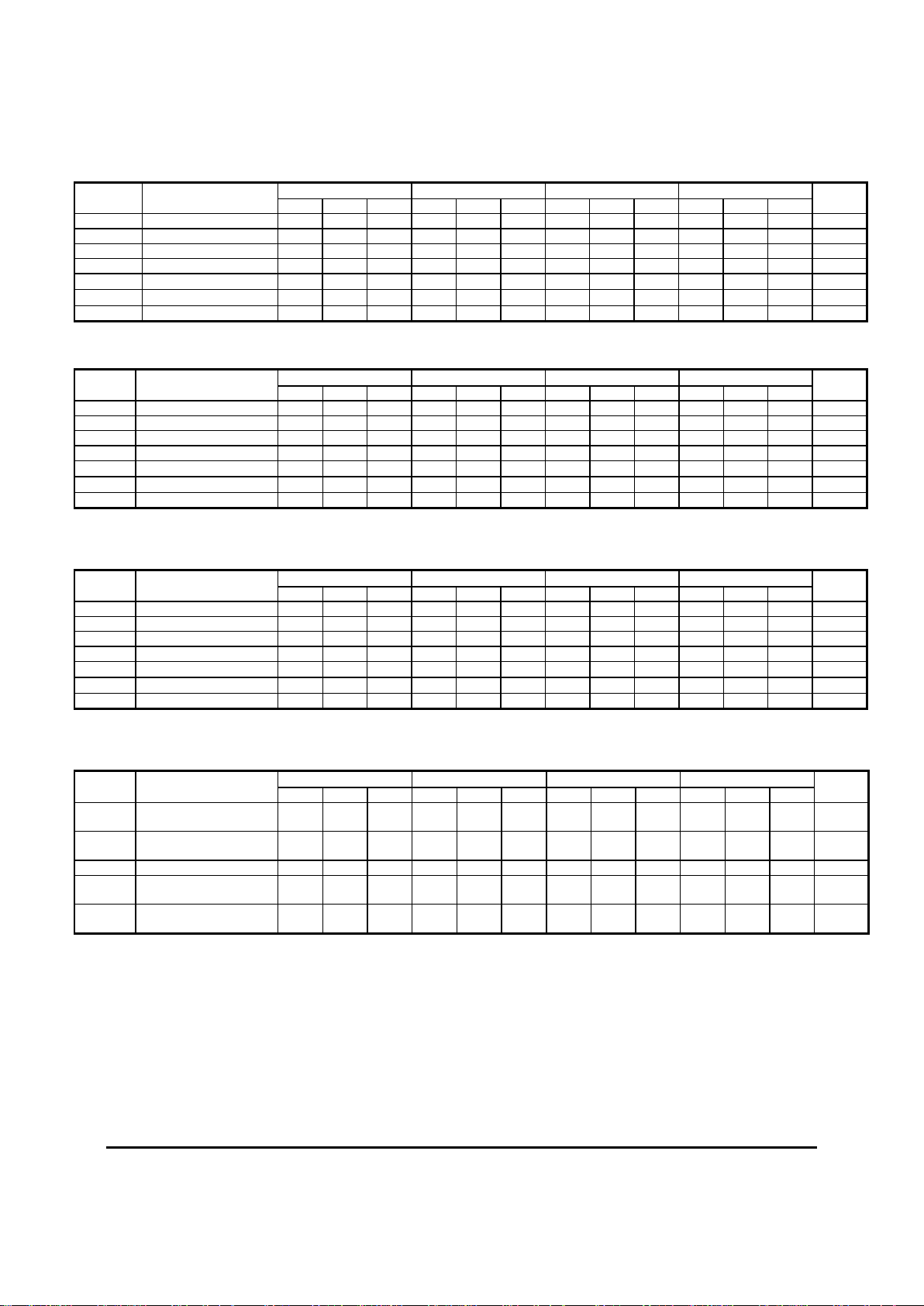
10K ECL DC Characteristics (VEE = -3.0V to -5.5V, VCC = GND)
-40°C 0°C 25°C 85°C
Symbol Characteristic
Min Typ Max Min Typ Max Min Typ Max Min Typ Max
Unit
VOH Output HIGH Voltage1 -1080 -890 -1020 -840 -980 -810 -910 -720 mV
VOL Output LOW Voltage1 -1950 -1650 -1950 -1630 -1950 -1630 -1950 -1595 mV
VIH Input HIGH Voltage -1230 -890 -1170 -840 -1130 -810 -1060 -720 mV
VIL Input LOW Voltage -1950 -1500 -1950 -1480 -1950 -1480 -1950 -1445 mV
IIL
Input LOW Current -150 -150 -150 -150
µA
IIH
Input HIGH Current 150 150 150 150
µA
IEE Power Supply Current 23 31 24 31 25 31 26 31 mA
1. Each output is terminated through a 50Ω resistor to V
CC
– 2V.
10K LVPECL DC Characteristics (VEE = GND, VCC = +3.3V)
-40°C 0°C 25°C 85°C
Symbol Characteristic
Min T
yp
Max Min T
yp
Max Min T
yp
Max Min T
yp
Max
Unit
VOH Output HIGH Voltage
1,2
2220 2410 2280 2460 2320 2490 2390 2580 mV
VOL Output LOW Voltage
1,2
1350 1650 1350 1670 1350 1670 1350 1705 mV
VIH Input HIGH Voltage1 2070 2410 2130 2460 2170 2490 2240 2580 mV
VIL Input LOW Voltage1 1350 1800 1350 1820 1350 1820 1350 1855 mV
IIL
Input LOW Current -150 -150 -150 -150
µA
IIH Input HIGH Current 150 150 150 150
µA
IEE Power Supply Current 23 31 24 31 25 31 26 31 mA
1. For supply voltages other that 3.3V, use the ECL table values and ADD supply voltage value.
2. Each output is terminated through a 50Ω resistor to V
CC
– 2V.
10K PECL DC Characteristics (VEE = GND, VCC = +5.0V)
-40°C 0°C 25°C 85°C
Symbol Characteristic
Min T
yp
Max Min T
yp
Max Min T
yp
Max Min T
yp
Max
Unit
VOH Output HIGH Voltage
1,2
3920 4110 3980 4160 4020 4190 4090 4280 mV
VOL Output LOW Voltage
1,2
3050 3350 3050 3370 3050 3370 3050 3405 mV
VIH Input HIGH Voltage1 3770 4110 3830 4160 3870 4190 3940 4280 mV
VIL Input LOW Voltage1 3050 3500 3050 3520 3050 3520 3050 3555 mV
IIL
Input LOW Current -150 -150 -150 -150
µA
IIH Input HIGH Current 150 150 150 150
µA
IEE Power Supply Current 23 31 24 31 25 31 26 31 mA
1. For supply voltages other that 5.0V, use the ECL table values and ADD supply voltage value.
2. Each output is terminated through a 50Ω resistor to V
CC
– 2V.
AZ10LVEL11
AZ100LVEL11
October 2001 * REV - 0 www.azmicrotek.com
3
100K ECL DC Characteristics (V
EE
= -3.0V to -5.5V, VCC = GND)
-40°C 0°C 25°C 85°C
Symbol Characteristic
Min Typ Max Min Typ Max Min Typ Max Min Typ Max
Unit
VOH Output HIGH Voltage1 -1085 -1005 -880 -1025 -955 -880 -1025 -955 -880 -1025 -955 -880 mV
VOL Output LOW Voltage1 -1830 -1695 -1555 -1810 -1705 -1620 -1810 -1705 -1620 -1810 -1705 -1620 mV
VIH Input HIGH Voltage -1165 -880 -1165 -880 -1165 -880 -1165 -880 mV
VIL Input LOW Voltage -1810 -1475 -1810 -1475 -1810 -1475 -1810 -1475 mV
IIL
Input LOW Current -150 -150 -150 -150
µA
IIH
Input HIGH Current 150 150 150 150
µA
IEE Power Supply Current 22 31 23 31 24 31 28 34 mA
1. Each output is terminated through a 50Ω resistor to V
CC
– 2V.
100K LVPECL DC Characteristics (VEE = GND, VCC = +3.3V)
-40°C 0°C 25°C 85°C
Symbol Characteristic
Min T
yp
Max Min T
yp
Max Min T
yp
Max Min T
yp
Max
Unit
VOH Output HIGH Voltage
1,2
2215 2295 2420 2275 2345 2420 2275 2345 2420 2275 2345 2420 mV
VOL Output LOW Voltage
1,2
1470 1605 1745 1490 1595 1680 1490 1595 1680 1490 1595 1680 mV
VIH Input HIGH Voltage1 2135 2420 2135 2420 2135 2420 2135 2420 mV
VIL Input LOW Voltage1 1490 1825 1490 1825 1490 1825 1490 1825 mV
IIL
Input LOW Current -150 -150 -150 -150
µA
IIH Input HIGH Current 150 150 150 150
µA
IEE Power Supply Current 22 31 23 31 24 31 28 34 mA
1. For supply voltages other that 3.3V, use the ECL table values and ADD supply voltage value.
2. Each output is terminated through a 50Ω resistor to V
CC
– 2V.
100K PECL DC Characteristics (VEE = GND, VCC = +5.0V)
-40°C 0°C 25°C 85°C
Symbol Characteristic
Min T
yp
Max Min T
yp
Max Min T
yp
Max Min T
yp
Max
Unit
VOH Output HIGH Voltage
1,2
3915 3995 4120 3975 4045 4120 3975 4045 4120 3975 4045 4120 mV
VOL Output LOW Voltage
1,2
3170 3305 3445 3190 3295 3380 3190 3295 3380 3190 3295 3380 mV
VIH Input HIGH Voltage1 3835 4120 3835 4120 3835 4120 3835 4120 mV
VIL Input LOW Voltage1 3190 3525 3190 3525 3190 3525 3190 3525 mV
IIL
Input LOW Current -150 -150 -150 -150
µA
IIH Input HIGH Current 150 150 150 150
µA
IEE Power Supply Current 22 31 23 31 24 31 28 34 mA
1. For supply voltages other that 5.0V, use the ECL table values and ADD supply voltage value.
2. Each output is terminated through a 50Ω resistor to V
CC
– 2V.
AC Characteristics (VEE = -3.0V to -5.5V, VCC = GND or VEE = GND, VCC = +3.0V to +5.5V)
-40°C 0°C 25°C 85°C
Symbol Characteristic
Min Typ Max Min Typ Max Min Typ Max Min Typ Max
Unit
t
PLH
/ t
PHL
Propagation Delay to
Output
135 260 335 185 260 335 190 265 340 215 310 365 ps
t
SKEW
Within-Device Skew 1
Duty Cycle Skew
2
5 5 5 5 20
20
5 5 20
20
5 5 20
20
ps
V
PP
(AC) Minimum Input Swing3 150 150 150 150 mV
V
CMR
Common Mode Range4
V
EE
+
1.2
VCC -
0.2
VEE +
1.2
VCC -
0.2
VEE +
1.2
VCC -
0.2
VEE +
1.2
VCC -
0.2
V
tr / tf
Rise/Fall Time
20 – 80%
100 260 100 260 100 260 100 260 ps
1. Within-device skew defined as identical transitions on similar paths through a device.
2. Duty cycle skew is the difference between a t
PLH
and t
PHL
propagation delay through a device.
3. V
PP
is the minimum peak-to-peak differential input swing for which AC parameters guaranteed. The device has a DC gain of ≈ 40.
4. The V
CMR
range is referenced to the most positive side of the differential input signal. Normal operation is obtained if the HIGH level falls within
the specified range and the peak-to-peak voltage lies between V
PP
(min) and 1V.
 Loading...