

AZMIC AZ100LVE310FNR2, AZ100LVE310FN Datasheet
ARIZONA MICROTEK, INC.
AZ100LVE310
ECL/PECL 2:8 Differential Clock Driver
FEATURES
• Operating Range of 3.0V to 5.5V
• Low Skew
• Guaranteed Skew Spec
• Differential Design
• V
Output
BB
PACKAGE PART NO. MARKING
PLCC 28 AZ100LVE310FN AZM100LVE310
PLCC 28 T&R AZ100LVE310FNR2 AZM100LVE310
• 75kΩ Internal Input Pulldown Resistors
• Direct Replacement for ON Semiconductor
MC100LVE310 & MC100E310
DESCRIPTION
The AZ100LVE310 is a low skew 2:8 fanout buffer designed with clock distribution in mind. The device
features fully differential clock paths to minimize both device and system skew. The AZ100LVE310 offers two
selectable clock inputs allowing redundant or test clocks to be incorporated into the system clock trees.
The AZ100LVE310 provides a V
device. For single–ended input applications, the V
differential input pair. The input signal is then fed to the other CLKa/CLKb input. The V
as a bias for the AZ100LVE310 as its current sink/source capability is limited. When used, the V
bypassed to ground via a 0.01µF capacitor.
Both sides of the differential output must be terminated into 50Ω to ensure that the tight skew specification is
met, even if only one side is used. In most applications all eight differential pairs will be used and therefore
terminated. In the case where fewer than eight pairs are used, all output pairs on the same package side (sharing the
same V
) as the pairs being used should be terminated to maintain minimum skew. Failure to do this will result in
CCO
small degradations of propagation delay (on the order of 10–20ps) of the outputs being used; while not being
catastrophic to most designs this will result in an increase in skew.
NOTE: Specifications in the ECL/PECL tables are valid when thermal equilibrium is established.
V
CLK_SEL
CLKa
V
CLKa
V
CLKb
EE
CC
BB
1630 S. STAPLEY DR., SUITE 125 • MESA, ARIZONA 85204 • USA • (480) 962-5881 • FAX (480) 890-2541
output for single-ended use or a DC bias reference for AC coupling to the
BB
reference should be connected to one side of the CLKa/CLKb
BB
V
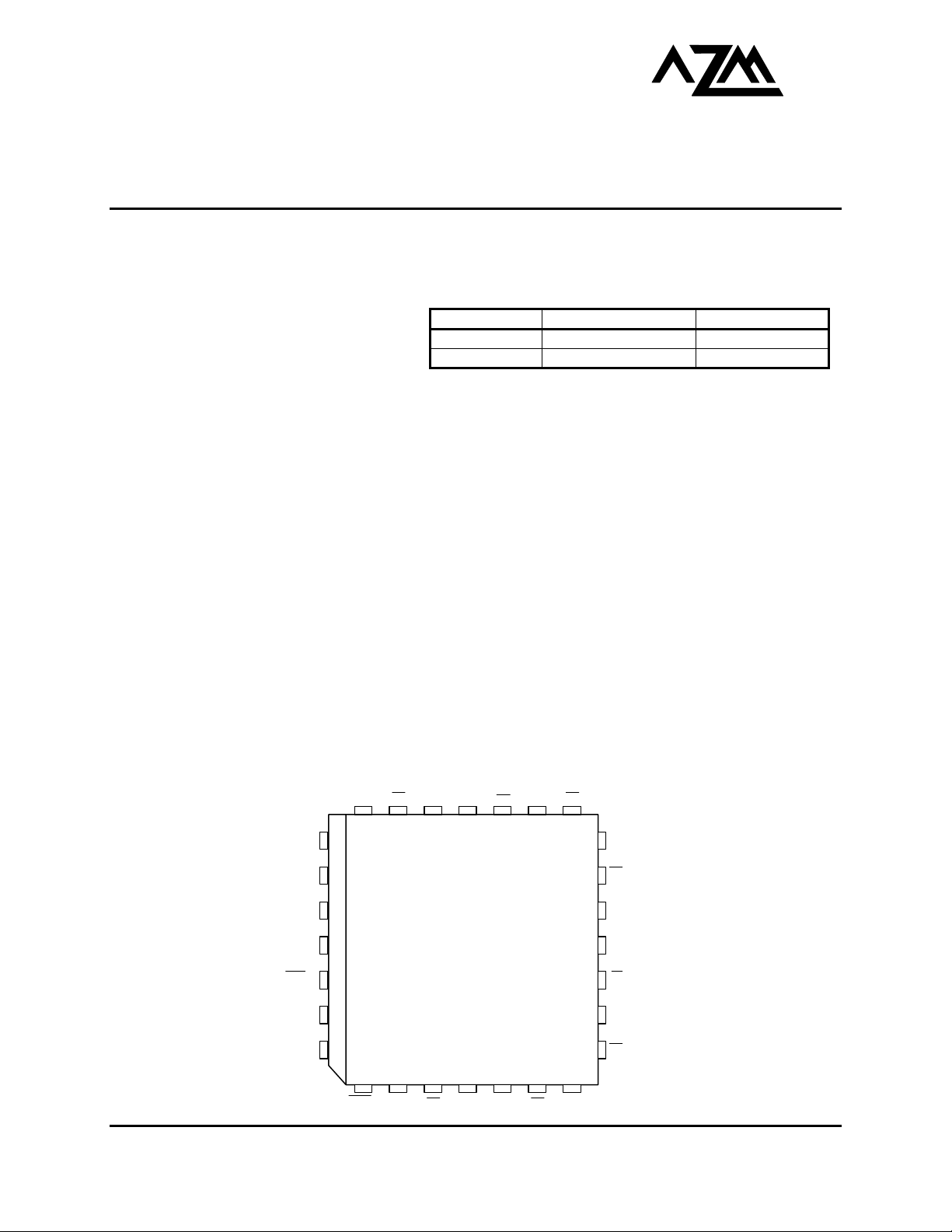
Q1 Q1Q0 Q0 Q2 Q2
CCO
25 24 23 22 21 20 19
26
27
28
1
Pinout: 28-Lead
PLCC (top view)
2
3
4
567 8 91011
CLKb
NC
V
Q7
CCO
www.azmicrotek.com
PACKAGE AVAILABILITY
Q3
18
Q3
17
Q4
16
15
V
CCO
Q4
14
Q5
13
Q5
12
Q7
Q6
Q6
pin should be used only
BB
pin should be
BB
AZ100LVE310
CLKa, CLKa ¯¯¯¯¯
CLKb, CLKb ¯¯¯¯¯
CLK_SEL Input Clock Select
Q0, Q0¯¯ – Q7, Q7¯¯ Differential Output Pairs
VBB VBB Output
VCC , V
V
EE
NC No Connect
CLK_SEL Input Clock
PIN DESCRIPTION
PIN FUNCTION
Differential Input Pairs
Differential Input Pairs
CCO
Positive Supply
Negative Supply
0
1
CLKa Selected
CLKb Selected
CLKa
CLKa
CLKb
CLKb
CLK_SEL
LOGIC SYMBOL
Q0
Q0
Q1
Q1
Q2
Q2
Q3
Q3
Q4
Q4
Q5
Q5
Q6
Q6
V
BB
Q7
Q7
Absolute Maximum Ratings are those values beyond which device life may be impaired.
Symbol Characteristic Rating Unit
VCC PECL Power Supply (VEE = 0V) 0 to +8.0 Vdc
VI PECL Input Voltage (V
VEE ECL Power Supply (VCC = 0V) -8.0 to 0 Vdc
VI ECL Input Voltage (VCC = 0V) -6.0 to 0 Vdc
I
OUT
TA Operating Temperature Range -40 to +85
T
STG
Output Current --- Continuous
--- Surge
Storage Temperature Range -65 to +150
100K ECL DC Characteristics (VEE = -3.0V to -5.5V, VCC = V
Symbol Characteristic
VOH Output HIGH Voltage1 -1085 -1005 -880 -1025 -955 -880 -1025 -955 -880 -1025 -955 -880 mV
VOL Output LOW Voltage1 -1830 -1695 -1555 -1810 -1705 -1620 -1810 -1705 -1620 -1810 -1705 -1620 mV
VIH Input HIGH Voltage -1165 -880 -1165 -880 -1165 -880 -1165 -880 mV
VIL Input LOW Voltage -1810 -1475 -1810 -1475 -1810 -1475 -1810 -1475 mV
VBB Reference Voltage -1380 -1260 -1380 -1260 -1380 -1260 -1380 -1260 mV
IIH
IIL
IEE Power Supply Current 55 60 55 60 55 60 65 70 mA
1. Each output is terminated through a 50Ω resistor to VCC – 2V.
Input HIGH Current 150 150 150 150
Input LOW Current 0.5 0.5 0.5 0.5
-40°C 0°C 25°C 85°C
Min Typ Max Min Typ Max Min Typ Max Min Typ Max
= 0V) 0 to +6.0 Vdc
EE
50
100
= GND)
CCO
mA
°C
°C
Unit
µA
µA
March 2002 * REV - 3 www.azmicrotek.com
2
 Loading...