

AZMIC AZ100ELT23TR2, AZ100ELT23TR1, AZ100ELT23T, AZ100ELT23DR2, AZ100ELT23DR1 Datasheet
...
AZ100ELT23
Dual Differential PECL to CMOS/TTL Translator
1630 S. STAPLEY DR., SUITE 125 • MESA, ARIZONA 85204 • USA • (480) 962-5881 • FAX (480) 890-2541
www.azmicrotek.com
ARIZONA MICROTEK, INC.
FEATURES
• 3.5ns Typical Propagation Delay
• <500ps Typical Output to Output Skew
• Differential PECL Inputs
• CMOS/TTL Outputs
• Flow Through Pinouts
• Direct Replacement for ON Semiconductor
MC100ELT23
• Operating Range of 3.0V to 5.5V (For operation
down to 2.5V supply consult AZM)
• Use AZ100ELT23 for 10K Applications
DESCRIPTION
The AZ100ELT23 is a dual differential PECL to CMOS/TTL translator. Because PECL (Positive ECL) levels
are used, only V
CC
and ground are required. The small outline 8-lead packaging and the low skew, dual gate design
of the ELT23 makes it ideal for applications that require the translation of a clock and a data signal.
The ELT23 is available in only the ECL 100K standard. Since there are no PECL outputs or an external V
BB
reference, the ELT23 does not require both ECL standard versions. The PECL inputs are differential; there is no
specified difference between the differential input 10K and 100K standards. Therefore the AZ100ELT23 can accept
any standard differential PECL input referenced from a V
CC
of 3.0V to 5.5V.
NOTE: Specifications in the ECL/PECL tables are valid when thermal equilibrium is established.
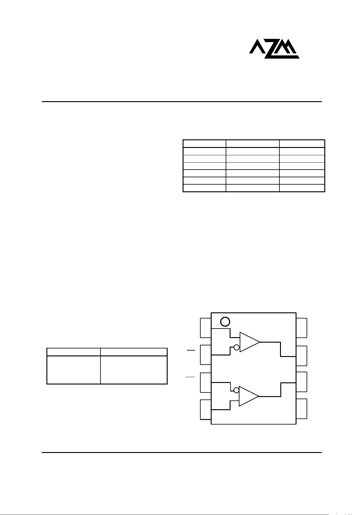
LOGIC DIAGRAM AND PINOUT ASSIGNMENT
PACKAGE AVAILABILITY
PACKAGE PART NO. MARKING
SOIC 8 AZ100ELT23D AZM100ELT23
SOIC 8 T&R AZ100ELT23DR1 AZM100ELT23
SOIC 8 T&R AZ100ELT23DR2 AZM100ELT23
TSSOP 8 AZ100ELT23T AZHLT23
TSSOP 8 T&R AZ100ELT23TR1 AZHLT23
TSSOP 8 T&R AZ100ELT23TR2 AZHLT23
PIN DESCRIPTION
PIN FUNCTION
Q0, Q1 CMOS/TTL Outputs
DO, D0¯¯ – D1, D1¯¯ Differential PECL inputs
VCC Positive Supply
GND Ground
8
5
6
7
4
3
2
1
V
CC
Q0
GND
D0
D0
D1
D1
Q1
PECL
CMOS/TTL
AZ100ELT23
March 2002 * REV - 3 www.azmicrotek.com
2
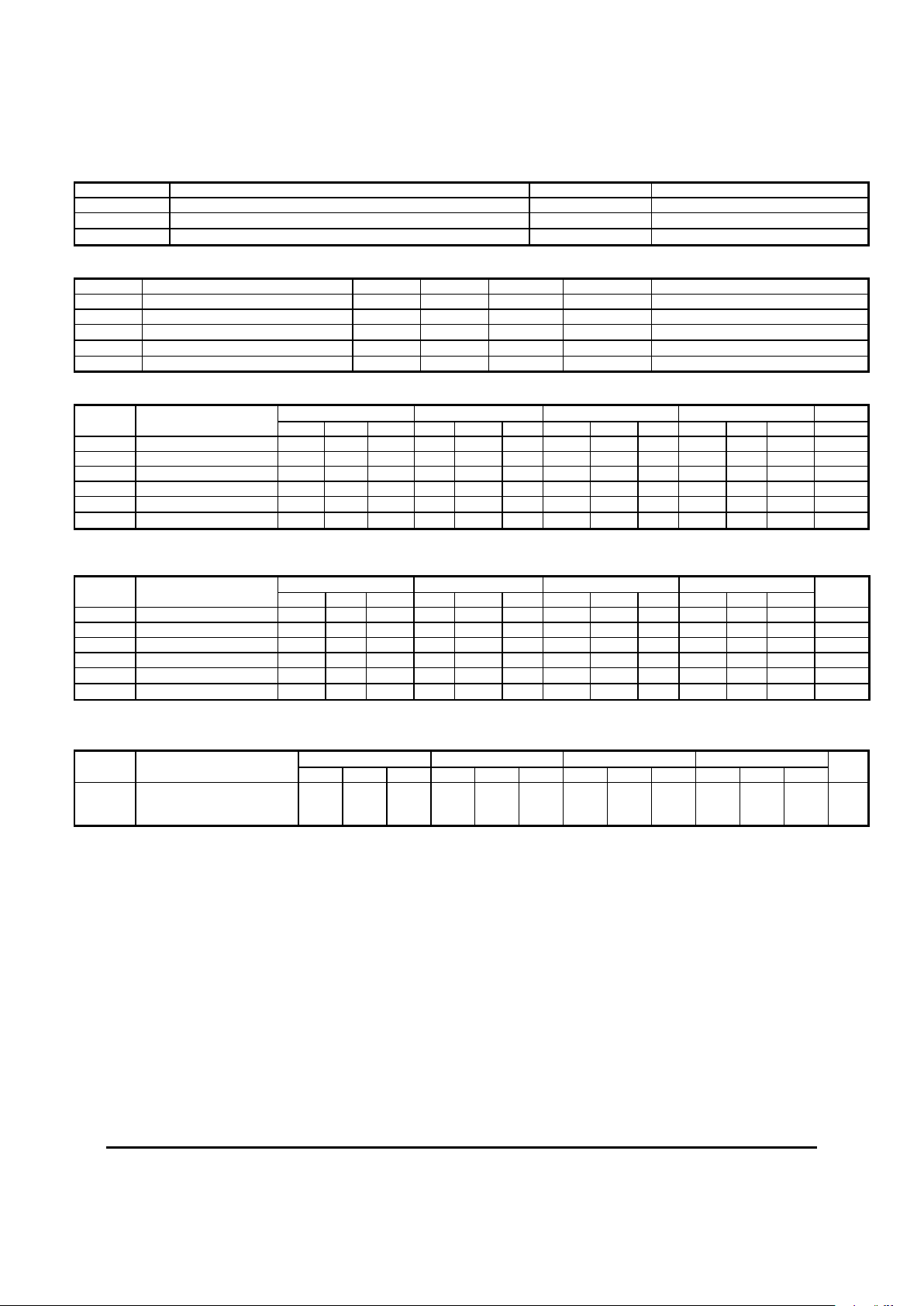
Absolute Maximum Ratings are those values beyond which device life may be impaired.
Symbol Character Value Unit
VCC DC Supply Voltage (Referenced to GND) 7.0 V
TA Operating Temperature Range (In Free-Air) -40 to+ 85
°C
T
STG
Storage Temperature Range -65 to +150
°C
CMOS/TTL DC CHARACTERISTICS (VCC = +3.0V to +5.5V)
Symbol Characteristic Min Typ Max Unit Condition
VOH Output HIGH Voltage V
CC
- 0.5 V IOH = -24 mA
VOL Output LOW Voltage 0.5 V IOL = 24 mA
ICC Power Supply Current 9.0 15 mA
0°C to 85°C
ICC Power Supply Current 9.0 17.6 mA
-40°C to 85°C
IOS Output Short Circuit Current 100 mA
100K LVPECL DC Characteristics (VCC = +3.3V)
-40°C 0°C 25°C 85°C
Unit
Symbol Characteristic
Min T
yp
Max Min T
yp
Max Min T
yp
Max Min T
yp
Max
VIH Input HIGH Voltage 2135 2420 2135 2420 2135 2420 2135 2420 mV
VIL Input LOW Voltage 1490 1825 1490 1825 1490 1825 1490 1825 mV
V
PP
Minimum Input Swing
1
200 200 200 200 mV
V
CMR
Common Mode Range 1.2 VCC 1.2 VCC 1.2 VCC 1.2 VCC V
IIL
Input LOW Current 0.5 0.5 0.5 0.5
µA
IIH Input HIGH Current 150 150 150 150
µA
1. 200mV input guarantees full logic swing at the output.
100K PECL DC Characteristics (VCC = +5.0V)
-40°C 0°C 25°C 85°C
Symbol Characteristic
Min T
yp
Max Min T
yp
Max Min T
yp
Max Min T
yp
Max
Unit
VIH Input HIGH Voltage 3835 4120 3835 4120 3835 4120 3835 4120 mV
VIL Input LOW Voltage 3190 3525 3190 3525 3190 3525 3190 3525 mV
V
PP
Minimum Input Swing
`1
200 200 200 200 mV
V
CMR
Common Mode Range 1.2 VCC 1.2 VCC 1.2 VCC 1.2 VCC V
IIL
Input LOW Current 0.5 0.5 0.5 0.5
µA
IIH Input HIGH Current 150 150 150 150
µA
1. 200mV input guarantees full logic swing at the output.
AC Characteristics (V
CC
= +3.0V to +5.5V)
-40°C 0°C 25°C 85°C
Symbol Characteristic
Min Typ Max Min Typ Max Min Typ Max Min Typ Max
Unit
t
PLH
/ t
PHL
Propagation Delay to Output
1
VCC = 4.5V to 5.5V
V
CC
= 3.0V to 3.6V
2.0
3.5
5.5
7.0
2.0
3.5
5.5
7.0
2.0
3.5
5.5
7.0
2.0
3.5
5.5
7.0
ns
1. CL=20pF
 Loading...