

AZMIC AZ100EL16VSTR1, AZ100EL16VST, AZ100EL16VSLR2, AZ100EL16VSLR1, AZ100EL16VSL Datasheet
...
ARIZONA MICROTEK, INC.
AZ100EL16VS
ECL/PECL Differential Receiver with Variable Output Swing
FEATURES
• 250ps Propagation Delay
• High Bandwidth Output Transitions
• 75kΩ Internal Input Pulldown Resistors
• Functionally Equivalent to ON
Semiconductor MC100EL16
• Variable Output Swing
• Available in a 3x3mm MLP Package
PACKAGE PART NO. MARKING
MLP 8 AZ100EL16VSL AZM16P
MLP 8 T&R AZ100EL16VSLR1 AZM16P
MLP 8 T&R AZ100EL16VSLR2 AZM16P
SOIC 8 AZ100EL16VSD AZM100EL16VS
SOIC 8 T&R AZ100EL16VSDR1 AZM100EL16VS
SOIC 8 T&R AZ100EL16VSDR2 AZM100EL16VS
TSSOP 8 AZ100EL16VST AZH16VS
TSSOP 8 T&R AZ100EL16VSTR1 AZH16VS
TSSOP 8 T&R AZ100EL16VSTR2 AZH16VS
PACKAGE AVAILABILITY
DESCRIPTION
The AZ100EL16VS is a differential receiver with variable output swing. The EL16VS has functionality and
output transition times similar to the EL16, with an input that controls the amplitude of the Q/Q¯ outputs. Maximum
swing is achieved by leaving the V
The operational range of the EL16VS control input, V
Simple control of the output swing can be obtained by a variable resistor between the V
wiper driving V
The EL16VS provides a V
For single-ended input applications, the V
pair. The input signal is then fed to the other D/D¯ input. The V
When used, the V
Under open input conditions (pulled to V
NOTE: Specifications in ECL/PECL tables are valid when thermal equilibrium is established.
. Typical application circuits and results are described in this Data Sheet.
CTRL
BB
pin should be bypassed to ground via a 0.01µF capacitor.
BB
pin open or tied to VEE.
CTRL
, is from VBB (full swing) to VCC (min. swing).
CTRL
output for single-ended use or a DC bias reference for AC coupling to the device.
reference should be connected to one side of the D/D¯ differential input
BB
pin can support 1.0mA sink/source current.
BB
) internal input clamps will force the Q output LOW.
EE
and VCC pins, with the
BB
1630 S. STAPLEY DR., SUITE 125 • MESA, ARIZONA 85204 • USA • (480) 962-5881 • FAX (480) 890-2541
www.azmicrotek.com
AZ100EL16VS
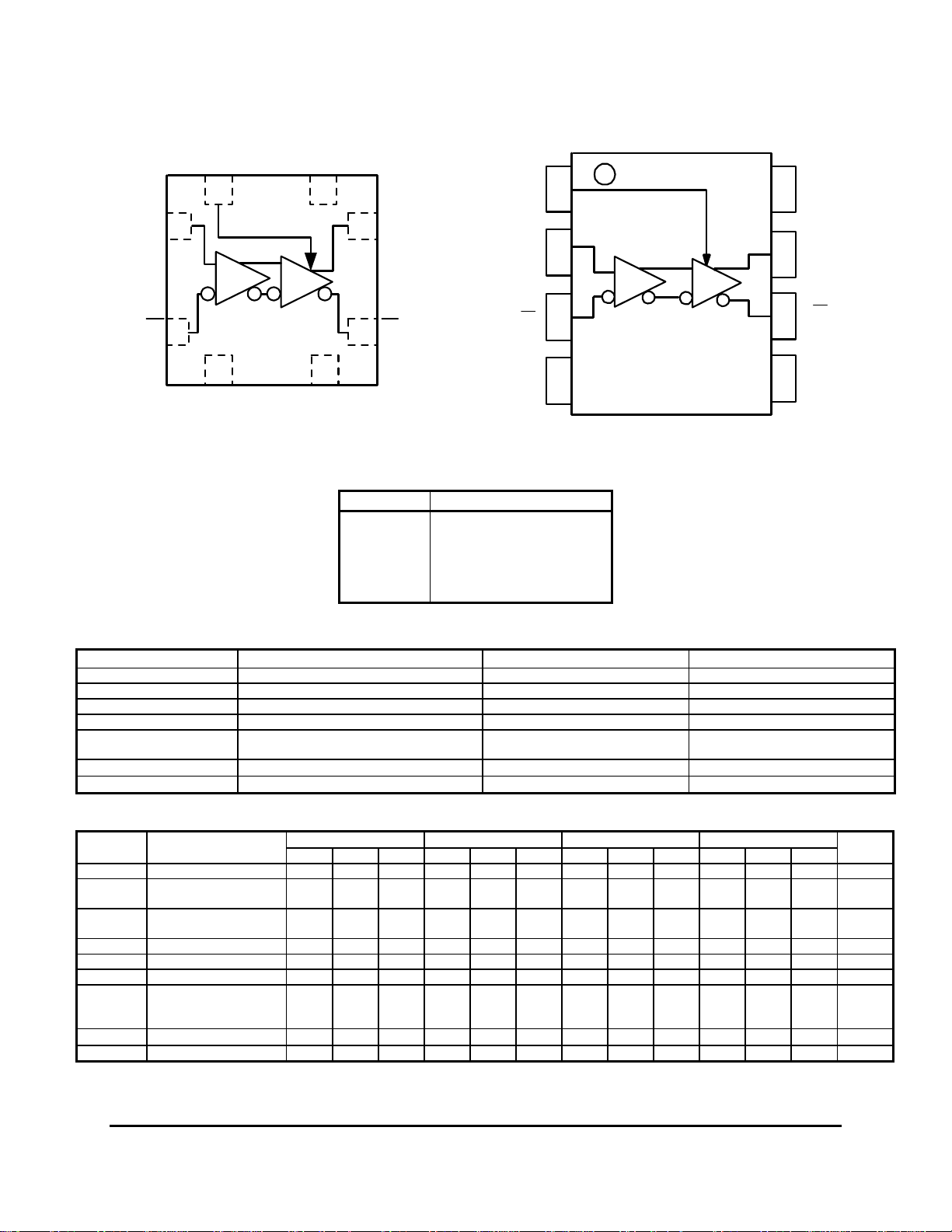
LOGIC DIAGRAM AND PINOUT ASSIGNMENT
V
CTRL
8
V
CC
7
V
CTRL
1
8
V
CC
1
D
Q
6
2
D
7
Q
Q
2
D
5
Q
3
D
6
3
V
BB
8 MLP (TOP VIEW)
Absolute Maximum Ratings are those values beyond which device life may be impaired.
Symbol Characteristic Rating Unit
VCC PECL Power Supply (VEE = 0V) 0 to +8.0 Vdc
VI PECL Input Voltage (V
VEE ECL Power Supply (VCC = 0V) -8.0 to 0 Vdc
VI ECL Input Voltage (VCC = 0V) -6.0 to 0 Vdc
I
OUT
TA Operating Temperature Range -40 to +85
T
STG
Output Current --- Continuous
--- Surge
Storage Temperature Range -65 to +150
4
V
EE
V
PIN DESCRIPTION
PIN FUNCTION
D, D¯ Data Inputs
V
Output Swing Control
CTRL
Q, Q¯ Data Outputs
VBB Reference Voltage Output
V
CC
Positive Supply
= 0V) 0 to +6.0 Vdc
EE
BB
4
8 SOIC & 8 TSSOP
50
100
5
mA
°C
°C
V
EE
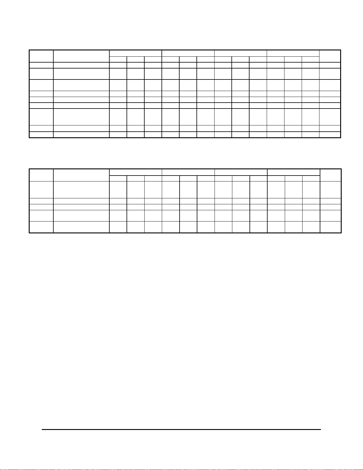
100K ECL DC Characteristics (V
Symbol Characteristic
VOH Output HIGH Voltage2 -1085 -880 -1025 -880 -1025 -955 -880 -1025 -880 mV
VOL
VOL
VIH Input HIGH Voltage -1165 -880 -1165 -880 -1165 -880 -1165 -880 mV
VIL Input LOW Voltage -1810 -1475 -1810 -1475 -1810 -1475 -1810 -1475 mV
VBB Reference Voltage -1420 -1260 -1420 -1260 -1420 -1260 -1420 -1260 mV
IIH
IIL
IEE Power Supply Current 18 25 18 25 18 25 21 26 mA
1. If V
2. Each output is terminated through a 50Ω resistor to V
Output LOW Voltage
V
= V
CTRL
CTRL
= V
BB
CC
Output LOW Voltage
V
Input HIGH Current
Input LOW Current 0.5 0.5 0.5 0.5
is Open Circuit, use the VOH (Max & Min) and VOL (V
CTRL
2
1
2
D, D¯
V
CTRL
= -4.2V to -5.5V, VCC = GND; V
EE
-40°C 0°C 25°C 85°C
Min Typ Max Min Typ Max Min Typ Max Min Typ Max
-1890 -1620 -1870 -1680 -1870 -1775 -1680 -1870 -1680 mV
-1180 -975 -1135 -990 -1135 -1065 -990 -1135 -990 mV
– 2V.
CC
150
40
= V
CTRL
: Max only) limits.
REF
CTRL
150
40
= VBB)
150
40
150
40
Unit
µA
µA
October 2001 * REV - 2 www.azmicrotek.com
2
yp
yp
yp
yp
AZ100EL16VS
100K PECL DC Characteristics (V
Symbol Characteristic
VOH Output HIGH Voltage
VOL
VOL
Output LOW Voltage
V
CTRL
Output LOW Voltage
V
CTRL
= V
= V
2
BB
CC
1,3
3915 4120 3975 4120 3975 4045 4120 3975 4120 mV
1,3
1,3
= GND, VCC = +5.0V)
EE
-40°C 0°C 25°C 85°C
Min T
Max Min T
Max Min T
Max Min T
Max
Unit
3110 3380 3130 3320 3130 3225 3320 3130 3320 mV
3820 4025 3865 4010 3865 3935 4010 3865 4010 mV
VIH Input HIGH Voltage1 3835 4120 3835 4120 3835 4120 3835 4120 mV
VIL Input LOW Voltage1 3190 3525 3190 3525 3190 3525 3190 3525 mV
VBB Reference Voltage1 3580 3740 3580 3740 3580 3740 3580 3740 mV
IIH
IIL
Input HIGH Current
D, D¯
V
CTRL
150
40
Input LOW Current 0.5 0.5 0.5 0.5
150
40
150
40
150
40
µA
µA
IEE Power Supply Current 18 25 18 25 18 25 21 26 mA
1. For supply voltages other that 5.0V, use the ECL table values and ADD supply voltage value.
2. If V
is Open Circuit, use the VOH (Max & Min) and VOL (V
CTRL
3. Each output is terminated through a 50Ω resistor to V
– 2V.
CC
CTRL
= V
: Max only) limits.
REF
AC Characteristics (V
Symbol Characteristic
t
PLH
t
SKEW
V
PP
V
CMR
tr / tf
1. Duty cycle skew is the difference between a t
2. V
3. The V
Input to Output Delay
/ t
PHL
Duty Cycle Skew1 (Diff) 5 5 20 5 20 5 20 ps
(AC) Minimum Input Swing2 150 150 150 150 mV
Common Mode Range3
Rise/Fall Time
20 – 80%
is the minimum peak-to-peak differential input swing for which AC parameters are guaranteed.
PP
range is referenced to the most positive side of the differential input signal. Normal operation is obtained if the HIGH level falls within
CMR
the specified range and the peak-to-peak voltage lies between V
= -4.2V to -5.5V; VCC =GND or VEE =GND; VCC = +4.2V to +5.5V)
EE
-40°C 0°C 25°C 85°C
Min Typ Max Min Typ Max Min Typ Max Min Typ Max
(Diff)
(SE)
V
CC
2.0
-
250
250
VCC -
175
125
VCC -
0.4
2.0
250
250
VCC -
325
375
0.4
175
125
VCC -
250
250
VCC -
2.0
100 350 100 350 100 350 100 350 ps
and t
PLH
propagation delay through a device.
PHL
(min) and 1V.
PP
325
375
0.4
205
155
VCC -
2.0
280
280
VCC -
355
405
0.4
Unit
ps
V
October 2001 * REV - 2 www.azmicrotek.com
3
 Loading...