

AZMIC AZ10E14FNR2, AZ10E14FN, AZ100E14FNR2, AZ100E14FN Datasheet
AZ10E142
AZ100E142
ECL/PECL 9-bit Shift Register
1630 S. STAPLEY DR., SUITE 125 • MESA, ARIZONA 85204 • USA • (480) 962-5881 • FAX (480) 890-2541
www.azmicrotek.com
ARIZONA MICROTEK, INC.
FEATURES
• 700 MHz Minimum Shift Frequency
• 9-Bit for Byte-Parity Application
• Asynchronous Master Reset
• Dual Clocks
• Operating Range of 4.2V to 5.46V
• 75kΩ Internal Input Pulldown Resistors
• Direct Replacement for ON Semiconductor
MC10E142 & MC100E142
DESCRIPTION
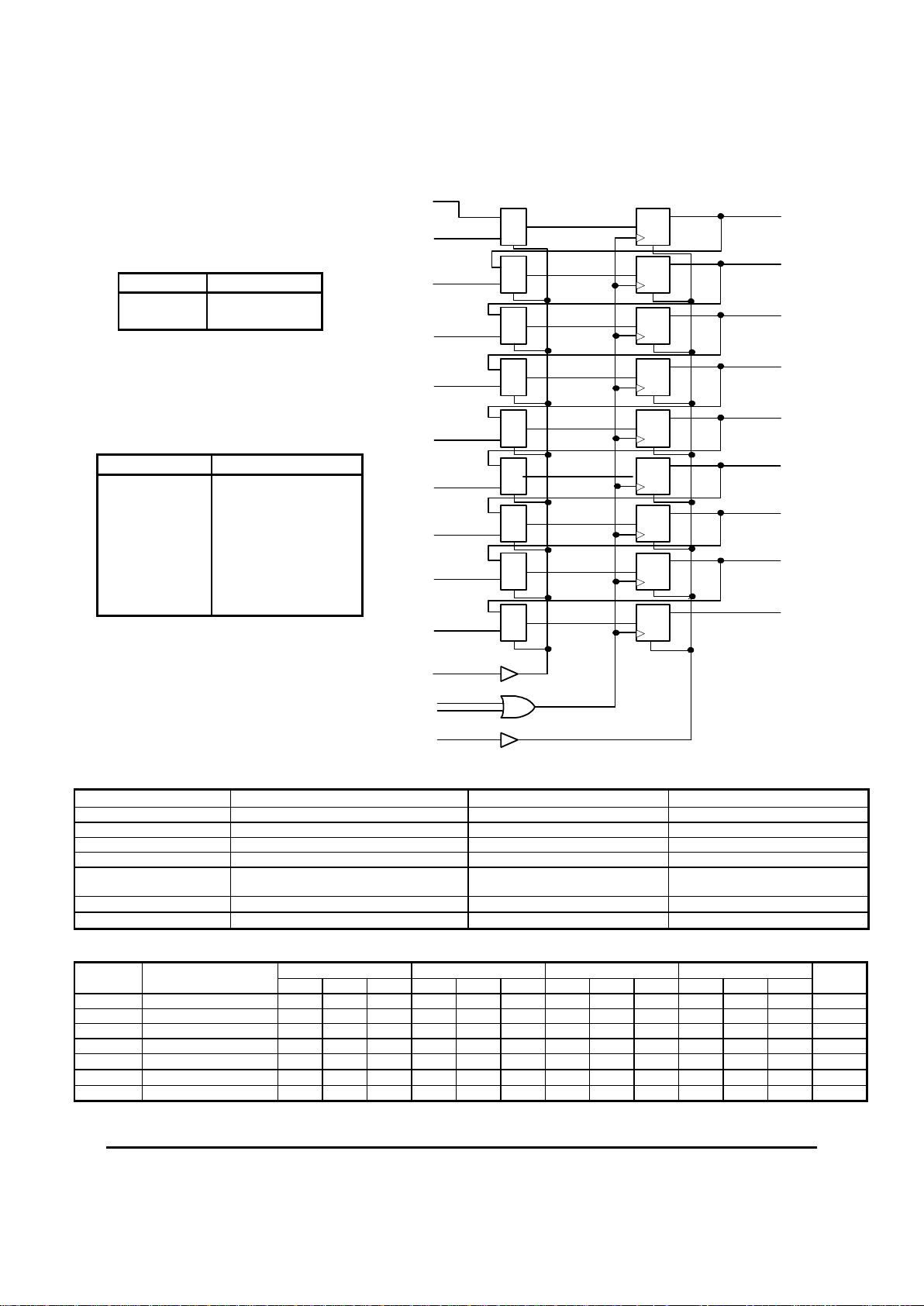
The AZ10/100E142 is a 9-bit shift register, designed with byte-parity applications in mind. The E142 performs
serial/parallel in and serial/parallel out, shifting in one direction. The nine inputs D0-D8 accept parallel input data,
while S-IN accepts serial input data. The Qn outputs do not need to be terminated for the shift operation to function.
To minimize noise and power, any Q output not used should be left unterminated.
The SEL (Select) input pin is used to switch between the two modes of operation
– SHIFT and LOAD. The shift
direction is from bit 0 to bit 8. Input data is accepted by the registers a set-up time before the positive going edge of
CLK1 or CLK2; shifting is also accomplished on the positive clock edge. A HIGH on the Master Reset pin (MR)
asynchronously resets all the registers to zero.
NOTE: Specifications in ECL/PECL tables are valid when thermal equilibrium is established.
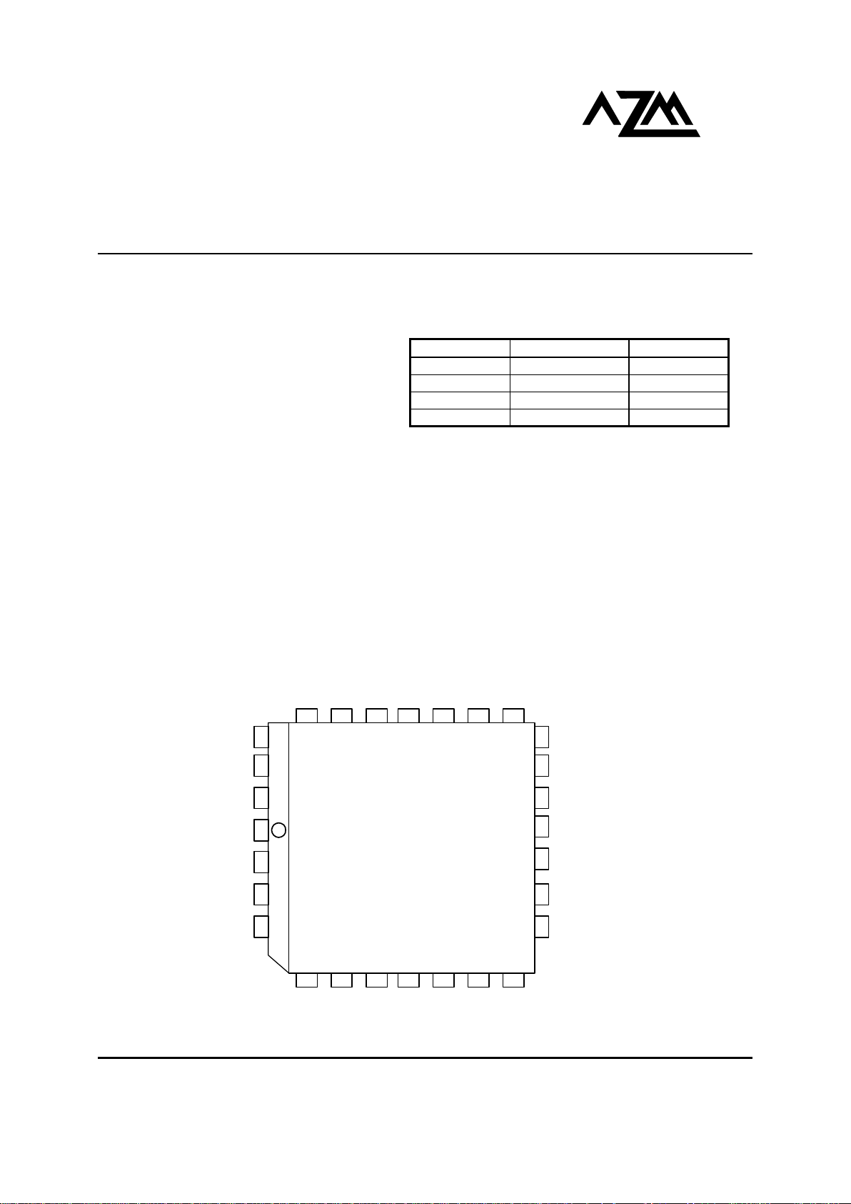
26
27
28
1
2
3
4
SEL D8 D7 D6
V
CCO
D5 Q8
Q7
Q6
V
CC
Q5
V
CCO
Q4
Q3
Q2Q1Q0
V
CCO
D4D3D2
MR
CLK1
CLK2
V
EE
S-IN
D0
D1
25 24 23 22 21 20 19
18
17
16
15
14
13
12
111098765
PACKAGE AVAILABILITY
PACKAGE PART NO. MARKING
PLCC 28 AZ10E142FN AZM10E142
PLCC 28 T&R AZ10E142FNR2 AZM10E142
PLCC 28 AZ100E142FN AZM100E142
PLCC 28 T&R AZ100E142FNR2 AZM100E142
Pinout: 28-lead
PLCC (top view)
AZ10E142
AZ100E142
October 2001 * REV - 2 www.azmicrotek.com
2
Absolute Maximum Ratings are those values beyond which device life may be impaired.
Symbol Characteristic Rating Unit
VCC PECL Power Supply (VEE = 0V) 0 to +8.0 Vdc
VI PECL Input Voltage (V
EE
= 0V) 0 to +6.0 Vdc
VEE ECL Power Supply (VCC = 0V) -8.0 to 0 Vdc
VI ECL Input Voltage (VCC = 0V) -6.0 to 0 Vdc
I
OUT
Output Current --- Continuous
--- Surge
50
100
mA
TA Operating Temperature Range -40 to +85
°C
T
STG
Storage Temperature Range -65 to +150
°C
10K ECL DC Characteristics (VEE = -4.94V to -5.46V, VCC = V
CCO
= GND)
-40°C 0°C 25°C 85°C
Symbol Characteristic
Min Typ Max Min Typ Max Min Typ Max Min Typ Max
Unit
VOH Output HIGH Voltage1 -1080 -890 -1020 -840 -980 -810 -910 -720 mV
VOL Output LOW Voltage1 -1950 -1650 -1950 -1630 -1950 -1630 -1950 -1595 mV
VIH Input HIGH Voltage -1230 -890 -1170 -840 -1130 -810 -1060 -720 mV
VIL Input LOW Voltage -1950 -1500 -1950 -1480 -1950 -1480 -1950 -1445 mV
IIH
Input HIGH Current 150 150 150 150
µA
IIL
Input LOW Current 0.5 0.5 0.5 0.5
µA
IEE Power Supply Current 120 145 120 145 120 145 120 145 mA
1. Each output is terminated through a 50Ω resistor to V
CC
– 2V.
LOGIC SYMBOL
1
0
1
0
1
0
1
0
1
0
1
0
1
0
1
0
1
0
Q
D
Q
D
Q
D
Q
D
Q
D
Q
D
Q
D
Q
D
Q
D
S-IN
D0
D1
D2
D3
D4
D5
D6
D7
D8
SEL
CLK1
CLK2
MR
Q0
Q1
Q2
Q3
Q4
Q5
Q6
Q7
Q8
PIN DESCRIPTION
PIN FUNCTION
D0 – D8 Parallel Data Inputs
S – IN Serial Data Input
SEL Mode Select Input
CLK1, CLK2 Clock Inputs
MR Master Reset
Q0 – Q8 Data Outputs
VCC , V
CCO
Positive Supply
V
EE
Negative Supply
FUNCTION TABLE
SEL MODE
L
H
Load
Shift
 Loading...