

AZMIC AZ10E131FNR2, AZ10E131FN, AZ100E131FNR2, AZ100E131FN Datasheet
AZ10E131
AZ100E131
ECL/PECL 4-bit D Flip-Flop
1630 S. STAPLEY DR., SUITE 125 • MESA, ARIZONA 85204 • USA • (480) 962-5881 • FAX (480) 890-2541
www.azmicrotek.com
ARIZONA MICROTEK, INC.
FEATURES
• 1100 MHz Min. Toggle Frequency
• Differential Outputs
• Individual and Common Clocks
• Individual Resets (asynchronous)
• Paired Sets (asynchronous)
• Operating Range of 4.2V to 5.46V
• 75kΩ Internal Input Pulldown Resistors
• Direct Replacement for On Semiconductor
MC10E131 & MC100E131
DESCRIPTION
The AZ10/100E131 is a quad master-slave D-type flip-flop with differential outputs. Each flip-flop may be
clocked separately by holding Common Clock (C
C
) LOW and using the Clock Enable (CE¯¯ n) inputs for clocking.
Common clocking is achieved by holding the CE¯¯ n inputs LOW and using C
C
to clock all four flip-flops. In this
case, the CE¯¯ n inputs perform the function of controlling the common clock to each flip-flop.
Individual asynchronous resets are provided (Rn). Asynchronous set controls (Sn) are ganged together in pairs,
with the pairing chosen to reflect physical chip symmetry.
Data enters the master when both C
C
and CE¯¯ n are LOW, and transfers to the slave when either CC or CE¯¯ n (or
both) go HIGH.
NOTE: Specifications in ECL/PECL tables are valid when thermal equilibrium is established.
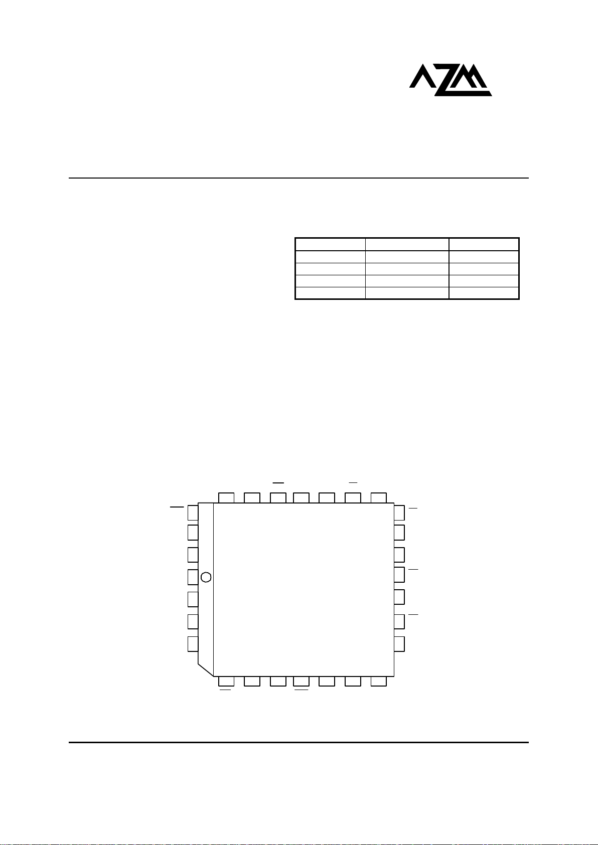
PACKAGE AVAILABILITY
PACKAGE PART NO. MARKING
PLCC 28 AZ10E131FN AZM10E131
PLCC 28 T&R AZ10E131FNR2 AZM10E131
PLCC 28 AZ100E131FN AZM100E131
PLCC 28 T&R AZ100E131FNR2 AZM100E131
26
27
28
1
2
3
4
V
CCO
V
CC
NC V
CCO
V
EE
25 24 23 22 21 20 19
18
17
16
15
14
13
12
111098765
R3 D2 CE2 R2 Q3 Q3
Q2
Q2
Q1
Q1
Q0
Q0
R1CE1D1R0CE0
D0
S03
C
C
S12
D3
CE3
* All VCC and V
CCO
pins are tied together on the die.
Pinout: 28-Lead
PLCC (top view)
AZ10E131
AZ100E131
October 2001 * REV - 2 www.azmicrotek.com
2
Absolute Maximum Ratings are those values beyond which device life may be impaired.
Symbol Characteristic Rating Unit
VCC PECL Power Supply (VEE = 0V) 0 to +8.0 Vdc
VI PECL Input Voltage (V
EE
= 0V) 0 to +6.0 Vdc
VEE ECL Power Supply (VCC = 0V) -8.0 to 0 Vdc
VI ECL Input Voltage (VCC = 0V) -6.0 to 0 Vdc
I
OUT
Output Current --- Continuous
--- Surge
50
100
mA
TA Operating Temperature Range -40 to +85
°C
T
STG
Storage Temperature Range -65 to +150
°C
10K ECL DC Characteristics (VEE = -4.94V to -5.46V, VCC = V
CCO
= GND)
-40°C 0°C 25°C 85°C
Symbol Characteristic
Min Typ Max Min Typ Max Min Typ Max Min Typ Max
Unit
VOH Output HIGH Voltage1 -1080 -890 -1020 -840 -980 -810 -910 -720 mV
VOL Output LOW Voltage1 -1950 -1650 -1950 -1630 -1950 -1630 -1950 -1595 mV
VIH Input HIGH Voltage -1230 -890 -1170 -840 -1130 -810 -1060 -720 mV
VIL Input LOW Voltage -1950 -1500 -1950 -1480 -1950 -1480 -1950 -1445 mV
IIH
Input HIGH Current
C
C
S
R,
CE¯¯
D
350
450
300
150
350
450
300
150
350
450
300
150
350
450
300
150
µA
IIL
Input LOW Current 0.5 0.5 0.5 0.5
µA
IEE Power Supply Current 58 70 58 70 58 70 58 70 mA
1. Each output is terminated through a 50Ω resistor to V
CC
– 2V.
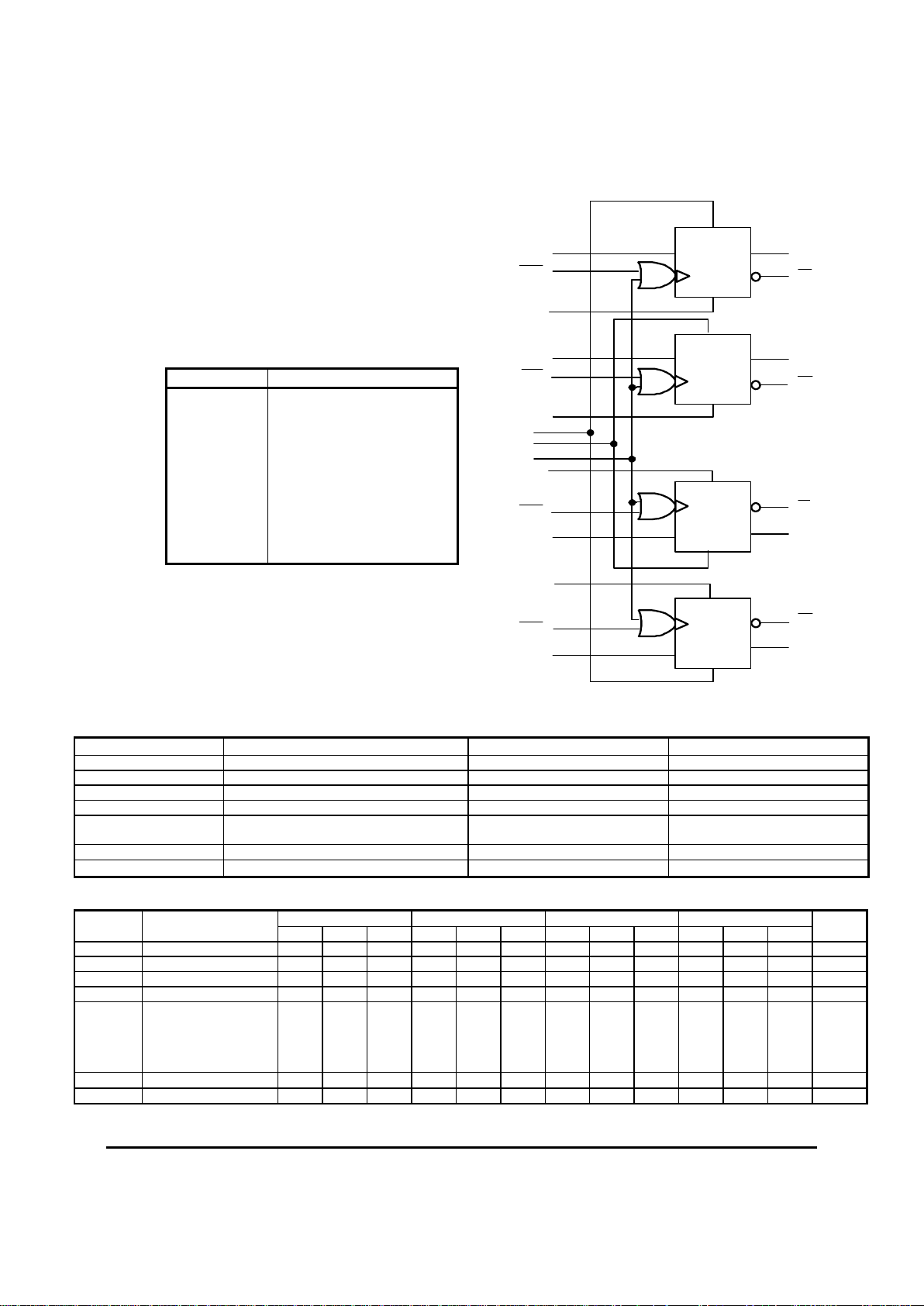
LOGIC SYMBOL
S
D
R
S
D
R
R
D
S
R
D
S
D3
D2
R2
R1
CE1
R0
CE0
D0
Q2
Q0
Q0
Q1
Q1
Q2
Q3
Q3
CE3
R3
CE2
S03
S12
C
C
D1
PIN DESCRIPTION
PIN FUNCTION
D0 – D3 Data inputs
CE0¯¯¯ – CE3¯¯¯ Clock Enables (Individual)
R0 – R3 Resets
CC Common Clock
S03,S12 Sets (paired)
Q0 – Q3 True Outputs
Q0¯¯ – Q3¯¯ Inverting Outputs
V
CC
, V
CCO
Positive Supply
V
EE
Negative Supply
NC No connect
 Loading...