

AZMIC AZ10E116FNR2, AZ10E116FN, AZ100E116FNR2, AZ100E116FN Datasheet
AZ10E116
AZ100E116
ECL/PECL Quint Differential Line Receiver
1630 S. STAPLEY DR., SUITE 125 • MESA, ARIZONA 85204 • USA • (480) 962-5881 • FAX (480) 890-2541
www.azmicrotek.com
ARIZONA MICROTEK, INC.
FEATURES
• 500ps Maximum Propagation Delay
• Dedicated V
CCO
Pin for Each Receiver
• Operating Range of 4.2V to 5.46V
• 75kΩ Internal Input Pulldown Resistors
• Direct Replacement for ON Semiconductor
MC10E116 & MC100E116
DESCRIPTION
The AZ10/100E116 is a quint differential line receiver with emitter-follower outputs. The E116 provides a VBB
output for single-ended use or a DC bias reference for AC coupling to the device. For single-ended input
applications, the V
BB
reference should be connected to one side of the Dn/D¯n differential input pair. The input
signal is then fed to the other Dn/D¯ n input. The V
BB
pin should be used only as a bias for the E116 as its sink/source
capability is limited. When used, the V
BB
pin should be bypassed to ground via a 0.01µF capacitor.
The receiver design features clamp circuitry to cause a defined state if both the inverting and non-inverting
inputs are left open; in this case the Q output goes LOW, while the Q¯ output goes HIGH. This feature makes the
device ideal for twisted pair applications.
If both inverting and non-inverting inputs are at an equal potential of > V
CC
-2.5V, the receiver does not go
to a defined state. This condition may produce output voltage levels between HIGH and LOW.
NOTE: Specifications in ECL/PECL tables are valid when thermal equilibrium is established.
PACKAGE AVAILABILITY
PACKAGE PART NO. MARKING
PLCC 28 AZ10E116FN AZM10E116
PLCC 28 T&R AZ10E116FNR2 AZM10E116
PLCC 28 AZ100E116FN AZM100E116
PLCC 28 T&R AZ100E116FNR2 AZM100E116
AZ10E116
AZ100E116
October 2001 * REV - 2 www.azmicrotek.com
2
Absolute Maximum Ratings are those values beyond which device life may be impaired.
Symbol Characteristic Rating Unit
VCC PECL Power Supply (VEE = 0V) 0 to +8.0 Vdc
VI PECL Input Voltage (V
EE
= 0V) 0 to +6.0 Vdc
VEE ECL Power Supply (VCC = 0V) -8.0 to 0 Vdc
VI ECL Input Voltage (VCC = 0V) -6.0 to 0 Vdc
I
OUT
Output Current --- Continuous
--- Surge
50
100
mA
TA Operating Temperature Range -40 to +85
°C
T
STG
Storage Temperature Range -65 to +150
°C
10K ECL DC Characteristics (VEE = -4.94V to -5.46V, VCC = V
CCO
= GND)
-40°C 0°C 25°C 85°C
Symbol Characteristic
Min Typ Max Min Typ Max Min Typ Max Min Typ Max
Unit
VOH Output HIGH Voltage1 -1080 -890 -1020 -840 -980 -810 -910 -720 mV
VOL Output LOW Voltage1 -1950 -1650 -1950 -1630 -1950 -1630 -1950 -1595 mV
VIH Input HIGH Voltage -1230 -890 -1170 -840 -1130 -810 -1060 -720 mV
VIL Input LOW Voltage -1950 -1500 -1950 -1480 -1950 -1480 -1950 -1445 mV
VBB Reference Voltage -1430 -1300 -1380 -1270 -1350 -1250 -1310 -1190 mV
IIH
Input HIGH Current 150 150 150 150
µA
IIL
Input LOW Current 0.5 0.5 0.5 0.5
µA
IEE Power Supply Current 29 35 29 35 29 35 29 35 mA
1. Each output is terminated through a 50Ω resistor to V
CC
– 2V.
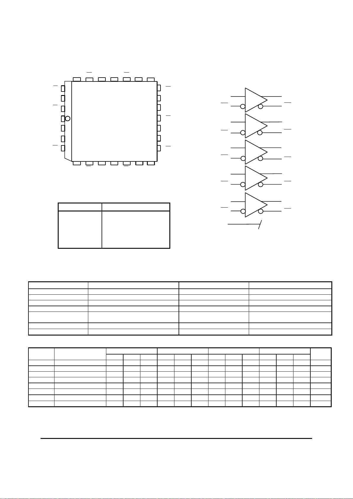
LOGIC SYMBOL
D0
D0
D1
D1
D2
D2
D3
D3
D4
D4
Q0
Q0
Q1
Q1
Q2
Q2
Q3
Q3
Q4
Q4
V
BB
26
27
28
1
2
3
4
V
CCO
V
CCO
V
EE
V
BB
V
CC
V
CCO
V
CCO
V
CCO
25
24 23 22
21
20
19
18
17
16
15
14
13
12
111098765
D3 D4 D4 Q4 Q4
Q3
Q3
Q2
Q2
Q1
Q1Q0Q0D1D1
D0
D0
D2
D2
D3
PIN DESCRIPTION
PIN FUNCTION
D0, D0¯¯ -D4, D4¯¯ Differential Input Pairs
Q0, Q0¯¯ -Q4, Q4¯¯ Differential Output Pairs
VBB Reference Voltage Output
V
CC
, V
CCO
Positive Supply
V
EE
Negative Supply
Pinout: 28-lead
PLCC (top view)
 Loading...