

AZMIC AZ10E111FNR2, AZ10E111FN, AZ100E111FNR2, AZ100E111FN Datasheet
AZ10E111
AZ100E111
ECL/PECL 1:9 Differential Clock Driver
1630 S. STAPLEY DR., SUITE 125 • MESA, ARIZONA 85204 • USA • (480) 962-5881 • FAX (480) 890-2541
www.azmicrotek.com
ARIZONA MICROTEK, INC.
FEATURES
• Low Skew
• Differential Design
• Clock Enable
• V
BB
Output
• Operating Range of 4.2V to 5.46V
• 75kΩ Internal Input Pulldown Resistors
• Direct Replacement for ON Semiconductor
MC10E111 & MC100E111
DESCRIPTION
The AZ10/100E111 is a low skew 1-to-9 differential driver, designed with clock distribution in mind. The IN
signal is fanned-out to nine identical differential outputs. An Enable input is also provided. A HIGH disables the
device by forcing all Q outputs LOW and all Q¯ outputs HIGH.
The AZ100E111 provides a V
BB
output for single-ended use or a DC bias reference for AC coupling to the
device. For single–ended input applications, the V
BB
reference should be connected to one side of the IN/IN¯¯
differential input pair. The input signal is then fed to the other IN/IN¯¯ input. The V
BB
pin should be used only as a
bias for the E111 as its sink/source capability is limited. When used, the V
BB
pin should be bypassed to ground via a
0.01µF capacitor.
The device is specifically designed, modeled and produced with low skew as the key goal. Optimal design and
layout serve to minimize gate-to-gate skew within-device, and empirical modeling is used to determine process
control limits that ensure consistent t
pd
distributions from lot-to-lot. The net result is a dependable, low skew device.
To ensure that the tight skew specification is met, both sides of the differential output must be terminated into
50Ω, even if only one side is used. In most applications all nine differential pairs will be used and therefore
terminated. In the case where fewer than nine pairs are used, it is necessary to terminate at least the output pairs on
the same package side (i.e. sharing the same V
CCO
) as the pair(s) being used on that side, in order to maintain
minimum skew. Failure to do this will result in small degradations of propagation delay (on the order of 10-20ps) of
the output(s) being used that, while not being catastrophic to most designs, will mean a loss of skew margin.
NOTE: Specifications in the ECL/PECL tables are valid when thermal equilibrium is established.
PACKAGE AVAILABILITY
PACKAGE PART NO. MARKING
PLCC 28 AZ10E111FN AZM10E111
PLCC 28 T&R AZ10E111FNR2 AZM10E111
PLCC 28 AZ100E111FN AZM100E111
PLCC 28 T&R AZ100E111FNR2 AZM100E111
AZ10E111
AZ100E111
October 2001 * REV - 2 www.azmicrotek.com
2
Absolute Maximum Ratings are those values beyond which device life may be impaired.
Symbol Characteristic Rating Unit
VCC PECL Power Supply (VEE = 0V) 0 to +8.0 Vdc
VI PECL Input Voltage (V
EE
= 0V) 0 to +6.0 Vdc
VEE ECL Power Supply (VCC = 0V) -8.0 to 0 Vdc
VI ECL Input Voltage (VCC = 0V) -6.0 to 0 Vdc
I
OUT
Output Current --- Continuous
--- Surge
50
100
mA
TA Operating Temperature Range -40 to +85
°C
T
STG
Storage Temperature Range -65 to +150
°C
10K ECL DC Characteristics (VEE = -4.94V to -5.46V, VCC = V
CCO
= GND)
-40°C 0°C 25°C 85°C
Symbol Characteristic
Min Typ Max Min Typ Max Min Typ Max Min Typ Max
Unit
VOH Output HIGH Voltage1 -1080 -890 -1020 -840 -980 -810 -910 -720 mV
VOL Output LOW Voltage1 -1950 -1650 -1950 -1630 -1950 -1630 -1950 -1595 mV
VIH Input HIGH Voltage -1230 -890 -1170 -840 -1130 -810 -1060 -720 mV
VIL Input LOW Voltage -1950 -1500 -1950 -1480 -1950 -1480 -1950 -1445 mV
VBB Reference Voltage -1430 -1300 -1380 -1270 -1350 -1250 -1310 -1190 mV
IIH
Input HIGH Current 150 150 150 150
µA
IIL
Input LOW Current 0.5 0.5 0.5 0.5
µA
IEE Power Supply Current 48 60 48 60 48 60 48 60 mA
1. Each output is terminated through a 50Ω resistor to V
CC
– 2V.
LOGIC SYMBOL
V
BB
IN
IN
EN
Q0
Q0
Q1
Q1
Q2
Q2
Q3
Q3
Q4
Q4
Q5
Q5
Q6
Q6
Q7
Q7
Q8
Q8
26
27
28
1
2
3
4
Q0 Q0 Q1 Q2
V
CCO
Q1 Q2
Q3
Q3
V
CC
Q5
V
CCO
Q5
Q6
Q6
Q7
V
CCO
Q8Q8
V
EE
IN
NC
25 24 23 22 21 20 19
18
17
16
15
14
13
12
111098765
V
BB
IN
EN
Q4
Q4
Q7
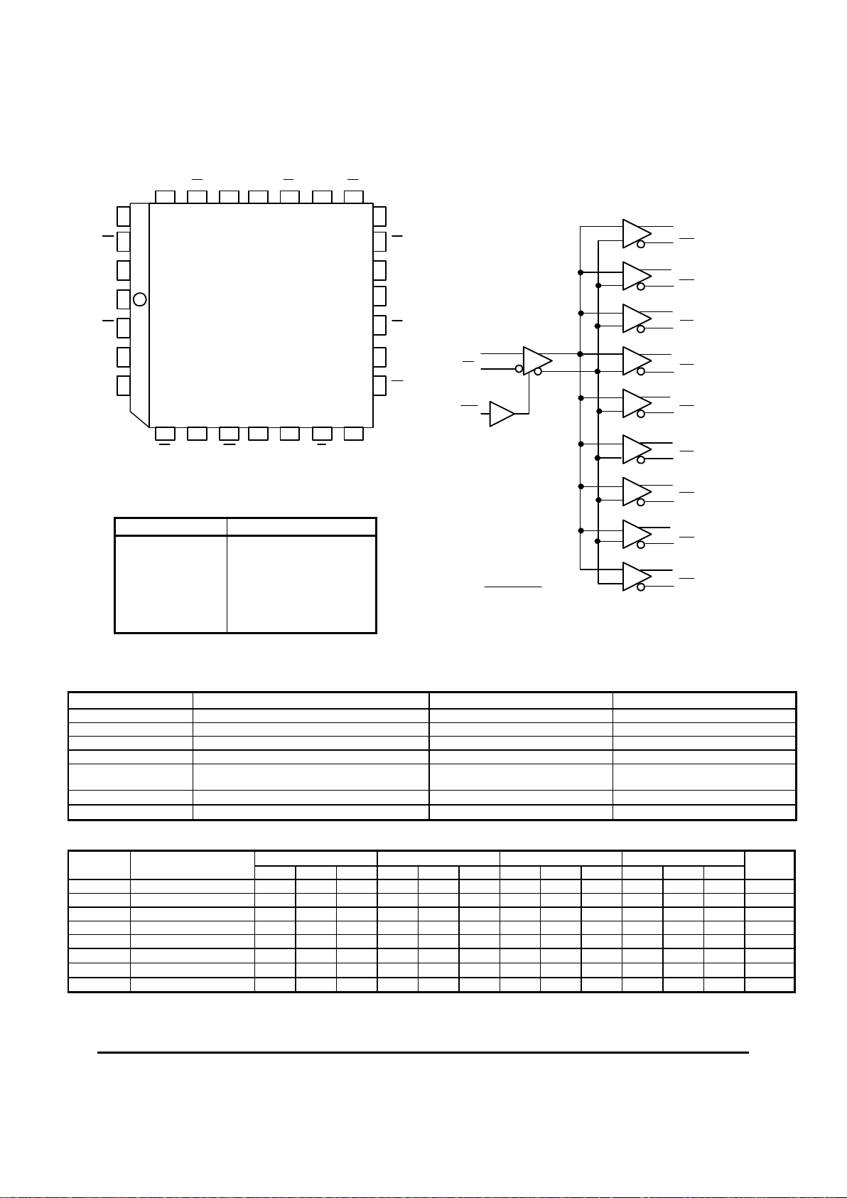
Pinout: 28-Lead PLCC
(Top Vi ew)
PIN DESCRIPTION
PIN FUNCTION
IN, IN¯¯ Differential Input Pair
EN¯¯ Enable
Q0, Q0¯¯ - Q8, Q8¯¯ Differential Outputs
VBB V
BB
Output
VCC , V
CCO
Positive Supply
V
EE
Negative Supply
 Loading...