

Page 1

PICO121
AMD G-Series Embedded SoC
Pico-ITX Board
User’s Manual
Page 2

ii
Disclaimers
This manual has been carefully checked and believed to contain accurate information.
Axiomtek Co., Ltd. assumes no responsibility for any infringements of patents or any third
party’s rights, and any liability arising from such use.
Axiomtek does not warrant or assume any legal liability or responsibility for the accuracy,
completeness or usefulness of any information in this document. Axiomtek does not make any
commitment to update the information in this manual.
Axiomtek reserves the right to change or revise this document and/or product at any time
without notice.
No part of this document may be reproduced, stored in a retrieval system, or transmitted, in
any form or by any means, electronic, mechanical, photocopying, recording, or otherwise,
without the prior written permission of Axiomtek Co., Ltd.
CAUTION
If you replace wrong batteries, it causes the danger of explosion. It is recommended by the
manufacturer that you follow the manufacturer’s instructions to only replace the same or
equivalent type of battery, and dispose of used ones.
Copyright 2014 Axiomtek Co., Ltd.
All Rights Reserved
April 2014, Version A1
Printed in Taiwan
Page 3

iii
ESD Precautions
Computer boards have integrated circuits sensitive to static electricity. To prevent chipsets
from electrostatic discharge damage, please take care of the following jobs with precautions:
Do not remove boards or integrated circuits from their anti-static packaging until you are
ready to install them.
Before holding the board or integrated circuit, touch an unpainted portion of the system
unit chassis for a few seconds. It discharges static electricity from your body.
Wear a wrist-grounding strap, available from most electronic component stores, when
handling boards and components.
Trademarks Acknowledgments
Axiomtek is a trademark of Axiomtek Co., Ltd.
Windows® is a trademark of Microsoft Corporation.
AMI is trademark of American Megatrend Inc.
IBM, PC/AT, PS/2, VGA are trademarks of International Business Machines Corporation.
AMD is trademark of AMD Corporation, Inc.
Other brand names and trademarks are the properties and registered brands of their
respective owners.
Page 4

iv
Table of Contents
Disclaimers ..................................................................................................... ii
ESD Precautions ........................................................................................... iii
Chapter 1 Introduction ............................................. 1
1.1 Features ............................................................................................... 2
1.2 Specifications ...................................................................................... 2
1.3 Utilities Supported .............................................................................. 3
Chapter 2 Board and Pin Assignments .................... 5
2.1 Board Dimensions and Fixing Holes ................................................. 5
2.2 Board Layout ....................................................................................... 7
2.3 Assembly Drawing .............................................................................. 9
2.4 Jumper Settings ................................................................................ 12
2.4.1 LVDS +12V Voltage Selection (JP1) (Optional) ........................................ 13
2.4.2 Auto Power On (JP2) ................................................................................ 13
2.4.3 LVDS +3.3V/+5V Voltage Selection (JP3) ................................................. 13
2.4.4 LVDS Brightness Control Mode Setting (JP4) .......................................... 13
2.4.5 DDR3/3L Voltage Selection (JP5) ............................................................. 14
2.4.6 RCC Enable (JP6) ..................................................................................... 14
2.4.7 Restore BIOS Optimal Defaults (JP7) ....................................................... 14
2.4.8 Buzzer Selection (CN1) ............................................................................. 14
2.5 Connectors ........................................................................................ 15
2.5.1 Power LED Header (CN3) ......................................................................... 16
2.5.2 High and Low Speed Board to Board Connectors (CN4 and CN5) .......... 16
2.5.3 SMBus Connector (CN6) .......................................................................... 18
2.5.4 Fan Power Connector (CN7) ..................................................................... 18
2.5.5 LVDS Connector (CN8) ............................................................................. 18
2.5.6 Serial ATA Power Connector (CN9) .......................................................... 20
2.5.7 Inverter Connector (CN10) ........................................................................ 20
2.5.8 SWIM Connector (CN11)........................................................................... 20
2.5.9 DC Power In Connector (CN12) ................................................................ 20
2.5.10 VGA Connector (CN13) ............................................................................. 21
2.5.11 Ethernet Connector (LAN1) ....................................................................... 21
2.5.12 Serial ATA Connector (SATA1) .................................................................. 22
2.5.13 CMOS Battery Connector (BAT1) ............................................................. 22
2.5.14 Full-size PCI-Express Mini Card and mSATA Connector (SCN1) ............. 23
2.5.15 SIM Card Slot (SCN2) ............................................................................... 24
2.5.16 Half-size PCI-Express Mini Card Connector (SCN3) ................................ 24
Page 5

v
Chapter 3 AX93277 I/O Board ................................ 25
3.1 AX93277 Specifications .................................................................... 25
3.2 AX93277 Dimensions and Fixing Holes .......................................... 25
3.3 AX93277 Board Layout ..................................................................... 27
3.4 AX93277 Jumper Settings ................................ ................................ 28
3.4.1 COM1 Data/Power Selection (JP1 and JP2) ............................................ 28
3.5 AX93277 Connectors, Switches and LED ....................................... 29
3.5.1 High and Low Speed Board to Board Connectors (CN2 and CN10) ........ 29
3.5.2 System Power Switch (CN5) ..................................................................... 31
3.5.3 COM Connector (CN6) .............................................................................. 31
3.5.4 Audio Jack (CN8) ...................................................................................... 31
3.5.5 System Reset Switch (CN9) ...................................................................... 32
3.5.6 USB 2.0 Connectors (USB1 and USB2) ................................................... 32
3.5.7 Power and HDD LED Indicator (D1) ......................................................... 32
Chapter 4 AX93267 I/O Board ................................ 33
4.1 AX93267 Specifications .................................................................... 33
4.2 AX93267 Dimensions and Fixing Holes .......................................... 34
4.3 AX93267 Board Layout ..................................................................... 35
4.4 AX93267 Connectors ........................................................................ 36
4.4.1 DC Power Jack (CN1) ............................................................................... 36
4.4.2 DC Power In Connector (CN2) .................................................................. 36
4.4.3 VGA Connector (CN3) ............................................................................... 37
4.4.4 D-Sub VGA Connector (CN4) ................................................................... 37
4.4.5 Ethernet Connector (CN5) ........................................................................ 38
4.4.6 RJ-45 Ethernet Port (CN6) ........................................................................ 38
Chapter 5 Hardware Description ........................... 39
5.1 Microprocessors ............................................................................... 39
5.2 BIOS ................................................................................................... 39
5.3 System Memory ................................................................................. 39
5.4 I/O Port Address Map ........................................................................ 40
5.5 Interrupt Controller (IRQ) Map ......................................................... 42
5.6 Memory Map ...................................................................................... 45
Chapter 6 AMI BIOS Setup Utility .......................... 47
6.1 Starting ............................................................................................... 47
6.2 Navigation Keys ................................................................................ 47
6.3 Main Menu .......................................................................................... 49
6.4 Advanced Menu ................................................................................. 50
Page 6

vi
6.5 Chipset Menu ..................................................................................... 60
6.6 Boot Menu .......................................................................................... 64
6.7 Security Menu .................................................................................... 65
6.8 Save & Exit Menu .............................................................................. 66
Chapter 7 Drivers Installation ................................ 69
7.1 Installing Chipset Driver ................................................................... 69
7.2 Installing Ethernet Driver .................................................................. 75
7.3 Installing Audio Driver ...................................................................... 78
Chapter 8 DASH User Guide ................................. 81
8.1 Client Side .......................................................................................... 81
8.1.1 BIOS Settings ............................................................................................ 81
8.1.2 Software Installation .................................................................................. 85
8.2 Console Side ..................................................................................... 85
8.2.1 Management Console Tool ....................................................................... 85
8.2.2 Built-in Web Server ................................................................................... 90
Appendix A AX93278 I/O Board (Optional) ............... 91
A.1 AX93278 Specifications .................................................................... 91
A.2 AX93278 Dimensions and Fixing Holes .......................................... 91
A.3 AX93278 Board Layout ..................................................................... 93
A.4 AX93278 Assembly Drawing ............................................................ 94
A.5 AX93278 Jumper Settings ................................ ................................ 95
A.5.1 COM1 Data/Power Selection (JP1 and JP2) ............................................ 95
A.6 AX93278 Connectors, Switches and LED ....................................... 96
A.6.1 High and Low Speed Board to Board Connectors (CN2 and CN1) .......... 96
A.6.2 Ethernet and USB 2.0 Connector (CN3) ................................................... 98
A.6.3 System Power Switch (CN4) ..................................................................... 98
A.6.4 USB 3.0 Connector (CN5) ......................................................................... 99
A.6.5 COM Connector (CN6) .............................................................................. 99
A.6.6 HDMI Connector (CN7) ........................................................................... 100
A.6.7 System Reset Switch (CN8) .................................................................... 100
A.6.8 Audio Connector (AUDIO1) ..................................................................... 100
A.6.9 Power and HDD LED Indicator (D1) ....................................................... 100
Appendix B Watchdog Timer ................................. 101
B.1 About Watchdog Timer ................................................................... 101
B.2 How to Use Watchdog Timer .......................................................... 101
B.3 Sample Program .............................................................................. 102
Page 7
PICO121 AMD G-Series Embedded SoC Pico-ITX Board
Introduction 1
Chapter 1
Introduction
The PICO121 is a Pico-ITX board with AMD G-Series Embedded SoC GX-210HA and
GX-210JA that delivers outstanding system performance through high-bandwidth interfaces,
multiple I/O functions for interactive applications and various embedded computing solutions.
The board has one 204-pin unbuffered SO-DIMM socket for DDR3/3L1333/1066MHz
SO-DIMM memory, maximum memory capacity up to 8GB. It also features one Gigabit/Fast
Ethernet, one SATA port with transfer rates up to 6Gb/s, four USB 2.0 high speed compliant,
and built-in high definition audio codec that can achieve the best stability and reliability for
industrial applications. Moreover, it has one full-size PCI-Express Mini Card and one half-size
PCI-Express Mini Card which provide good expansions for network connecting. Additionally, it
provides you with unique embedded features, such as two serial ports (one RS-232/422/485
and one RS-232) and Pico-ITX form factor that applies an extensive array of PC peripherals.
The board can be enhanced by its built-in watchdog timer function, a special industrial feature
not commonly seen on other motherboards.
Page 8

PICO121 AMD G-Series Embedded SoC Pico-ITX Board
2 Introduction
1.1 Features
AMD G-Series embedded SoC GX-210HA and GX-210JA
1 DDR3/3L SO-DIMM supports up to 8GB memory capacity
4 USB 2.0 ports
2 COM ports
1 full-size PCI-Express Mini Card
1 half-size PCI-Express Mini Card
DASH (Desktop and mobile Architecture for System Hardware) support
+12V only DC-in supported
1.2 Specifications
CPU
AMD G-Series embedded SoC dual core GX-210HA 1.0GHz.
AMD G-Series embedded SoC dual core GX-210JA 1.0GHz
Thermal Solution
Passive but with reserved fan connector.
BIOS
American Megatrends Inc. UEFI (Unified Extensible Firmware Interface) BIOS.
16Mbit SPI Flash, DMI, Plug and Play.
RPL/PXE Ethernet Boot ROM.
System Memory
One 204-pin unbuffered DDR3/3L SO-DIMM socket.
Maximum up to 8GB DDR3/3L 1333/1066MHz memory.
Onboard Multi I/O
Controller: Fintek F81801U.
Serial Ports: One port for RS-232/422/485 and one port for RS-232 in pin headers.
Serial ATA
One SATA-600 connector.
Expansion
One full-size PCI-Express Mini Card.
One half-size PCI-Express Mini Card.
One board-to-board connector, including two USB 3.0, one PCI Expressx1 and one
DisplayPort.
USB Interface
Four USB ports with fuse protection and comply with USB Spec. Rev. 2.0 in pin
headers.
Display
One 16-pin VGA wafer connector.
One 2x20-pin connector for 18-bit/24-bit single/dual channel LVDS and one 8-pin
wafer connector for inverter control. LVDS resolution is up to 1920x1200.
Page 9

PICO121 AMD G-Series Embedded SoC Pico-ITX Board
Introduction 3
Watchdog Timer
1~255 seconds or minutes; up to 255 levels.
Ethernet
One 16-pin wafer connector.
One port with Realtek RTL8111DP for Gigabit/Fast Ethernet.
Audio
HD audio compliant with Realtek ALC662.
MIC-in and line-out in pin headers.
Power Input
One 1x4-pin wafer connector.
+12V only DC-in.
AT auto power on function supported.
Power Management
ACPI (Advanced Configuration and Power Interface).
Form Factor
Pico-ITX form factor.
Note
All specifications and images are subject to change without notice.
1.3 Utilities Supported
Chipset and graphics driver
Ethernet driver (RTL8111DP)
Audio driver
Realtek Management Console Tool
Page 10

PICO121 AMD G-Series Embedded SoC Pico-ITX Board
4 Introduction
This page is intentionally left blank.
Page 11
PICO121 AMD G-Series Embedded SoC Pico-ITX Board
Board and Pin Assignments 5
Chapter 2
Board and Pin Assignments
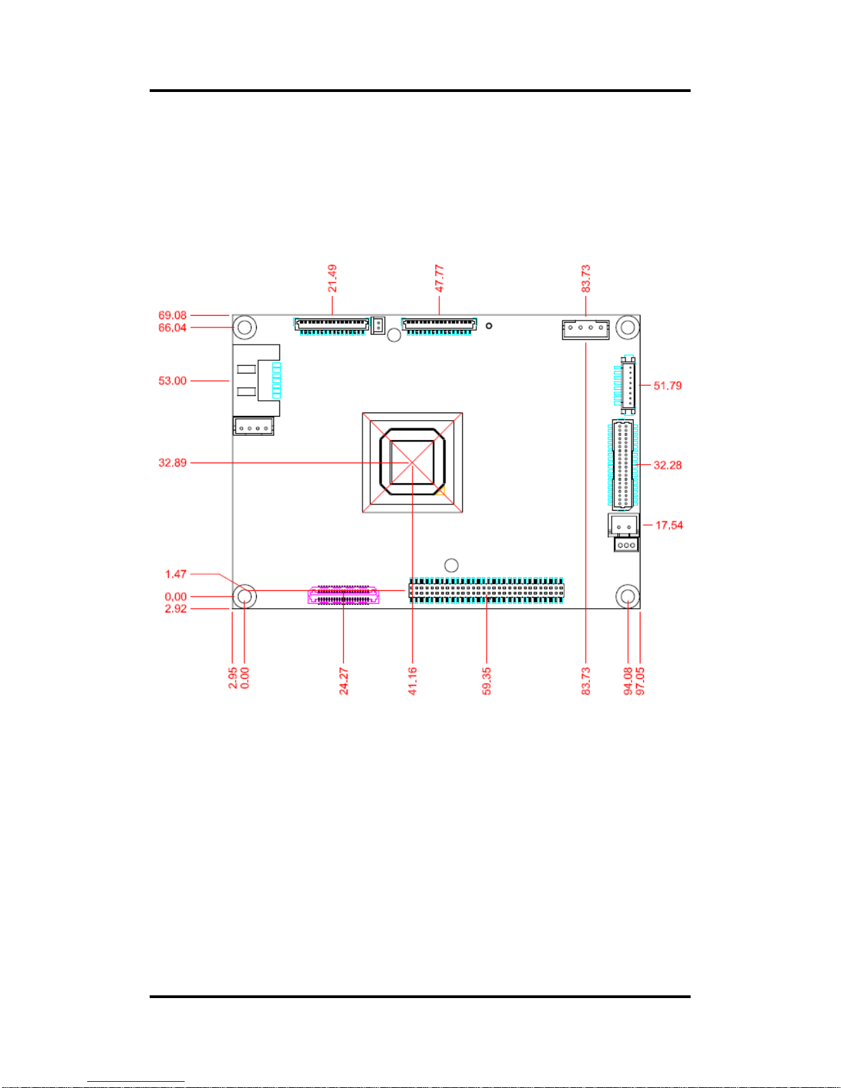
2.1 Board Dimensions and Fixing Holes
Top View
Page 12
PICO121 AMD G-Series Embedded SoC Pico-ITX Board
6 Board and Pin Assignments
Bottom View
Side View
Page 13
PICO121 AMD G-Series Embedded SoC Pico-ITX Board
Board and Pin Assignments 7
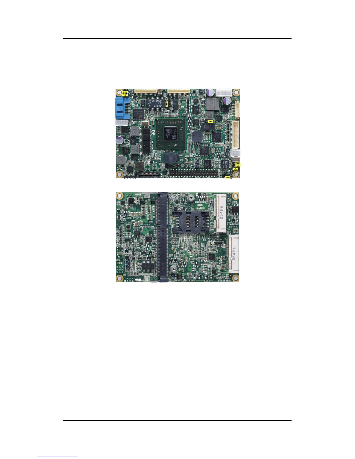
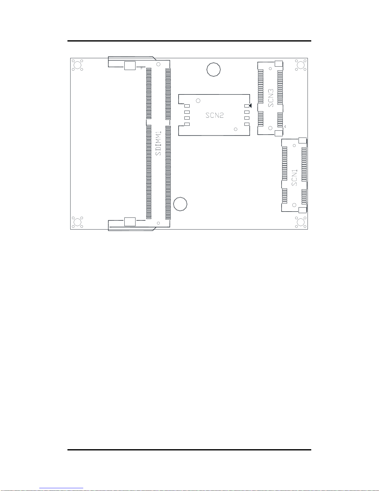
2.2 Board Layout
Top View
Page 14
PICO121 AMD G-Series Embedded SoC Pico-ITX Board
8 Board and Pin Assignments
Bottom View
Page 15
PICO121 AMD G-Series Embedded SoC Pico-ITX Board
Board and Pin Assignments 9
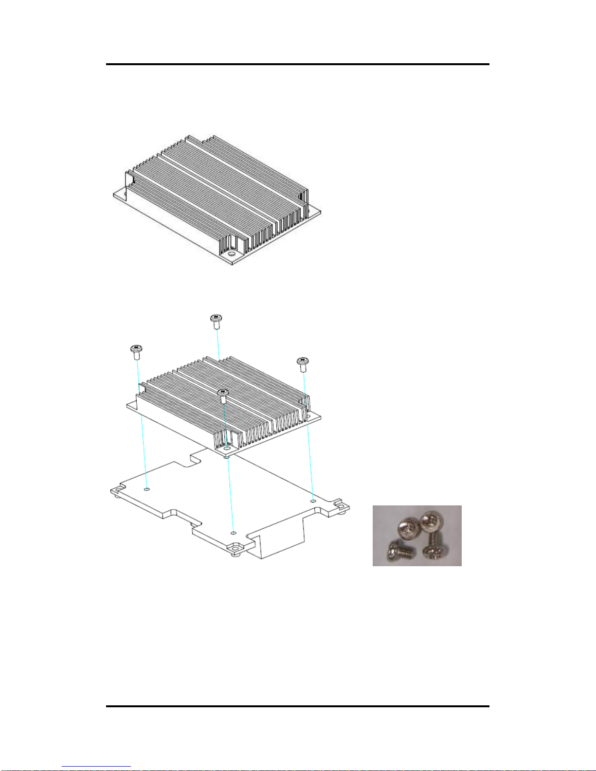
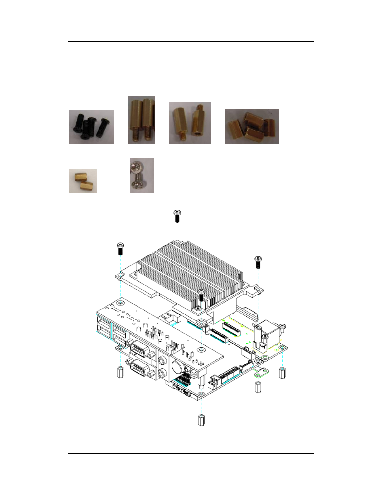
2.3 Assembly Drawing
Heatsink for PICO121 (see image below):
First of all, screw heatsink into heatspreader.
x4
Page 16
PICO121 AMD G-Series Embedded SoC Pico-ITX Board
10 Board and Pin Assignments
For thermal dissipation, a heatspreader enables the PICO121’s components to dissipate heat
efficiently. Images below illustrate how to install the heatspreader.
Installing Heatspreader
The PICO121 has four assembly holes for installing heatspreader plate. Align and firmly
secure heatspreader plate to PICO121. Be careful not to over-tighten the screws.
x4 x4 x4 (8mm)
Page 17
PICO121 AMD G-Series Embedded SoC Pico-ITX Board
Board and Pin Assignments 11
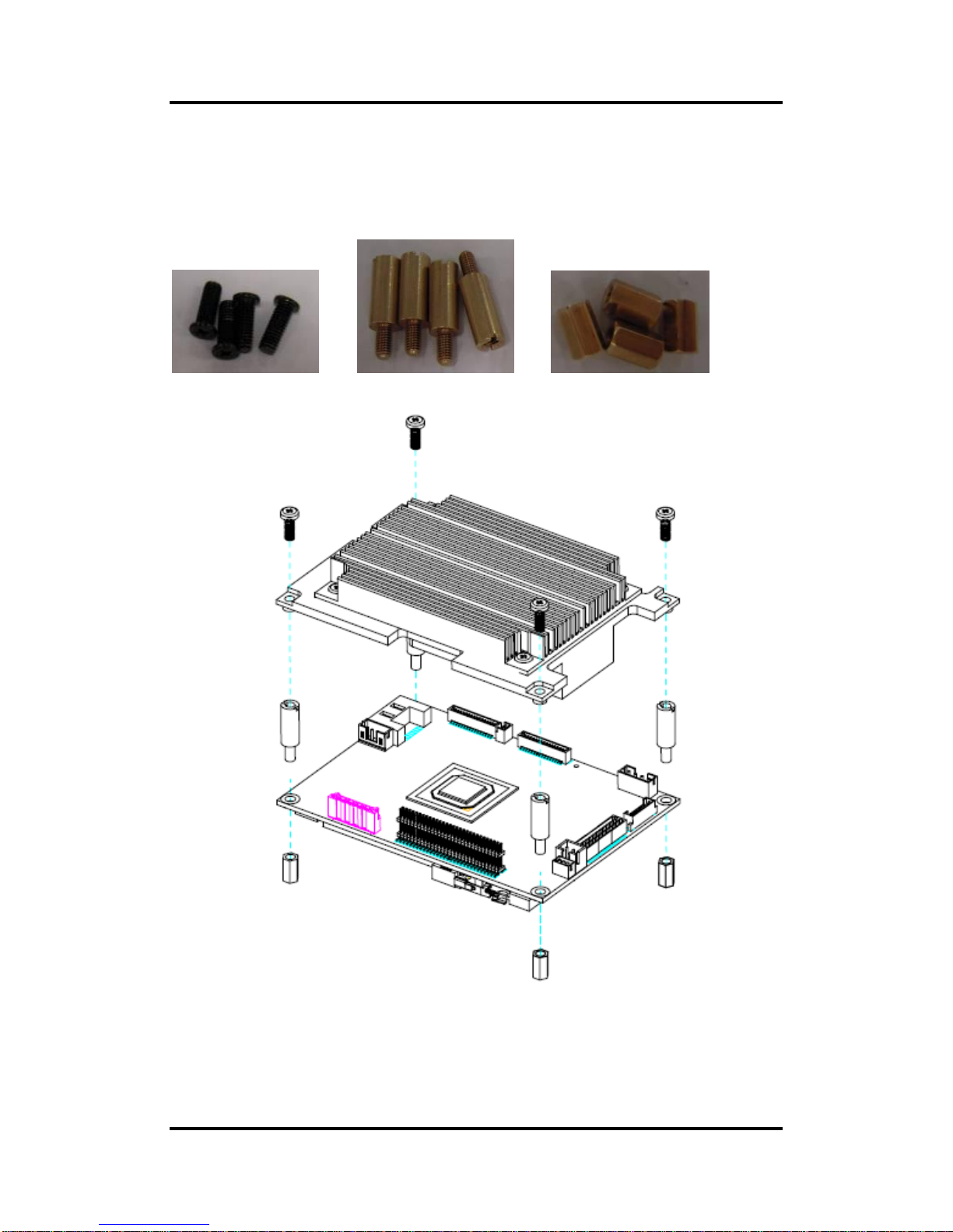
Installing Heatspreader and I/O Boards
Gently connect AX93277 and AX93267 I/O boards to PICO121. Align assembly holes and
firmly secure the heatspreader plate and I/O boards to the PICO121, see image below. Be
careful not to over-tighten the screws. See chapter 3 and chapter 4 for details of AX93277 and
AX93267 I/O boards, respectively.
x4 x2 x2 x4 (8mm)
x2 (7mm) x4
AX93277
PICO121
AX93267
Page 18
PICO121 AMD G-Series Embedded SoC Pico-ITX Board
12 Board and Pin Assignments
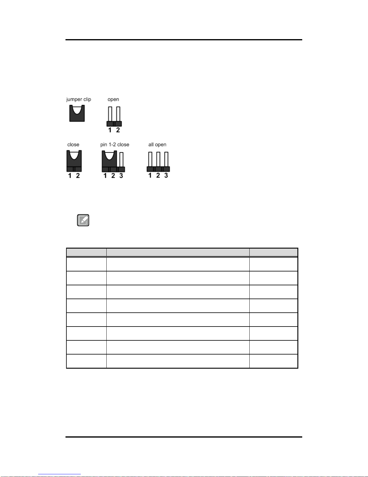
2.4 Jumper Settings
Jumper is a small component consisting of jumper clip and jumper pins. Install jumper clip on 2
jumper pins to close. And remove jumper clip from 2 jumper pins to open. Below illustration
shows how to set up jumper.
Properly configure jumper settings on the PICO121 to meet your application purpose. Below
you can find a summary table of all jumpers and onboard default settings.
Note
Once the default jumper setting needs to be changed, please do it under power-off
condition.
Jumper
Description
Setting
JP1 (Optional)
LVDS +12V Voltage Selection
Default: NA
Open
JP2
Auto Power On
Default: Disable
1-2 Close
JP3
LVDS +3.3V/+5V Voltage Selection
Default: +3.3V
1-2 Close
JP4
LVDS Brightness Control Mode Setting
Default: PWM Mode
1-2 Close
JP5
DDR3/3L Voltage Selection
Default: +1.5V
1-2 Close
JP6
RCC Enable
Default: Enable
1-2 Close
JP7
Restore BIOS Optimal Defaults
Default: Normal Operation
1-2 Close
CN1
Buzzer Selection
Default: Internal Buzzer
2-3 Close
Page 19
PICO121 AMD G-Series Embedded SoC Pico-ITX Board
Board and Pin Assignments 13
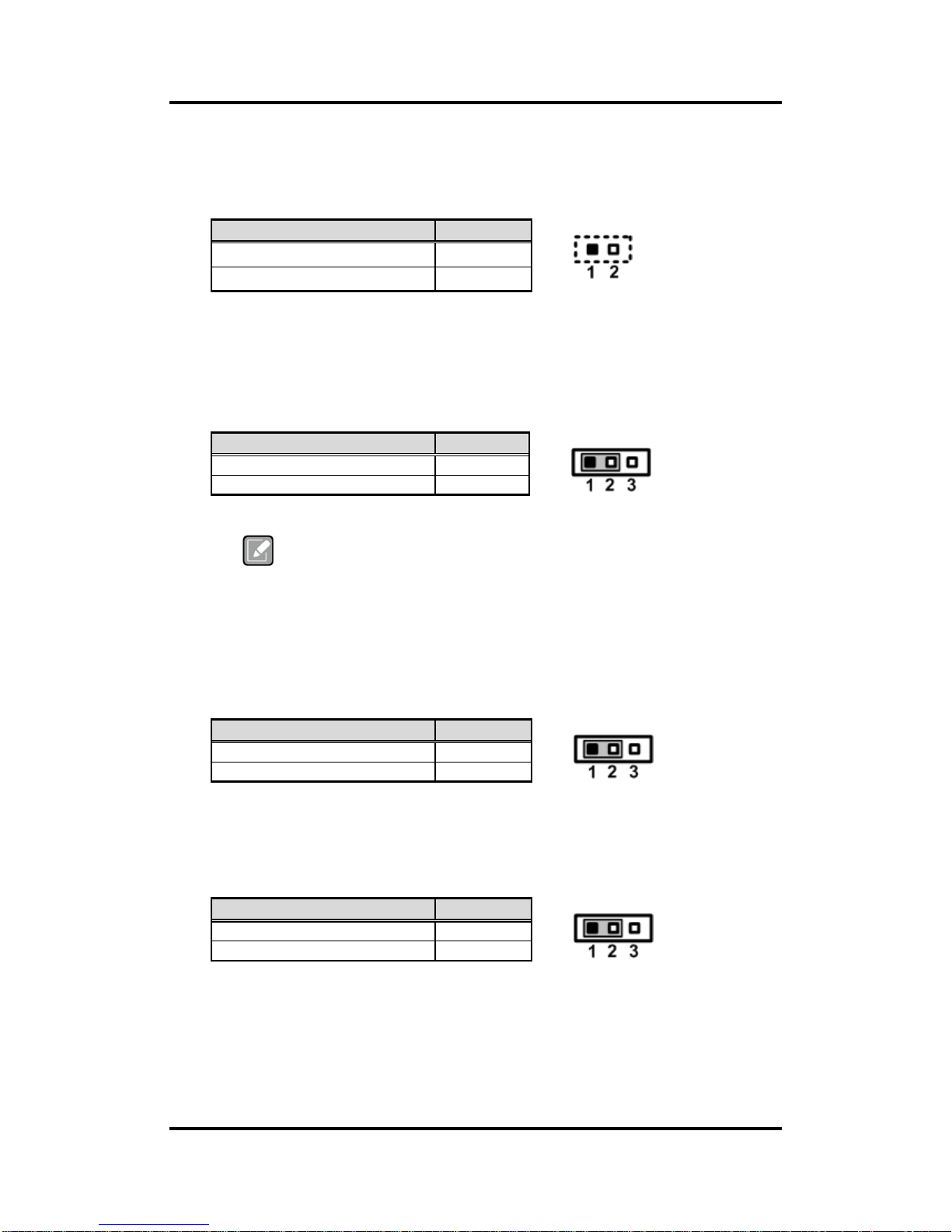
2.4.1 LVDS +12V Voltage Selection (JP1) (Optional)
The board supports voltage selection for flat panel displays. Use JP1 to set LVDS
connector (CN8) pin 1~6 VCCM to +12V. To prevent hardware damage, before
connecting please make sure that the input voltage of flat panel is correct.
2.4.2 Auto Power On (JP2)
If this jumper is enabled for AC power input, the system will be automatically power on
without pressing soft power button. If this jumper is disabled for AC power input, it is
necessary to manually press soft power button to power on the system.
Note
This function is similar to the feature of power on after power failure,
which is controlled by hardware circuitry instead of BIOS.
2.4.3 LVDS +3.3V/+5V Voltage Selection (JP3)
The board supports voltage selection for flat panel displays. Use JP3 to set LVDS
connector (CN8) pin 1~6 VCCM to +3.3V or +5V. To prevent hardware damage, before
connecting please make sure that the input voltage of flat panel is correct.
2.4.4 LVDS Brightness Control Mode Setting (JP4)
This jumper enables you to select PWM or voltage control mode for inverter connector
(CN10). These two control modes are for adjusting the brightness of LVDS panel.
Function
Setting
+12V
Close
NA (Default)
Open
Function
Setting
Disable auto power on (Default)
1-2 close
Enable auto power on
2-3 close
Function
Setting
+3.3V (Default)
1-2 close
+5V
2-3 close
Function
Setting
PWM mode (Default)
1-2 close
Voltage mode
2-3 close
Page 20
PICO121 AMD G-Series Embedded SoC Pico-ITX Board
14 Board and Pin Assignments
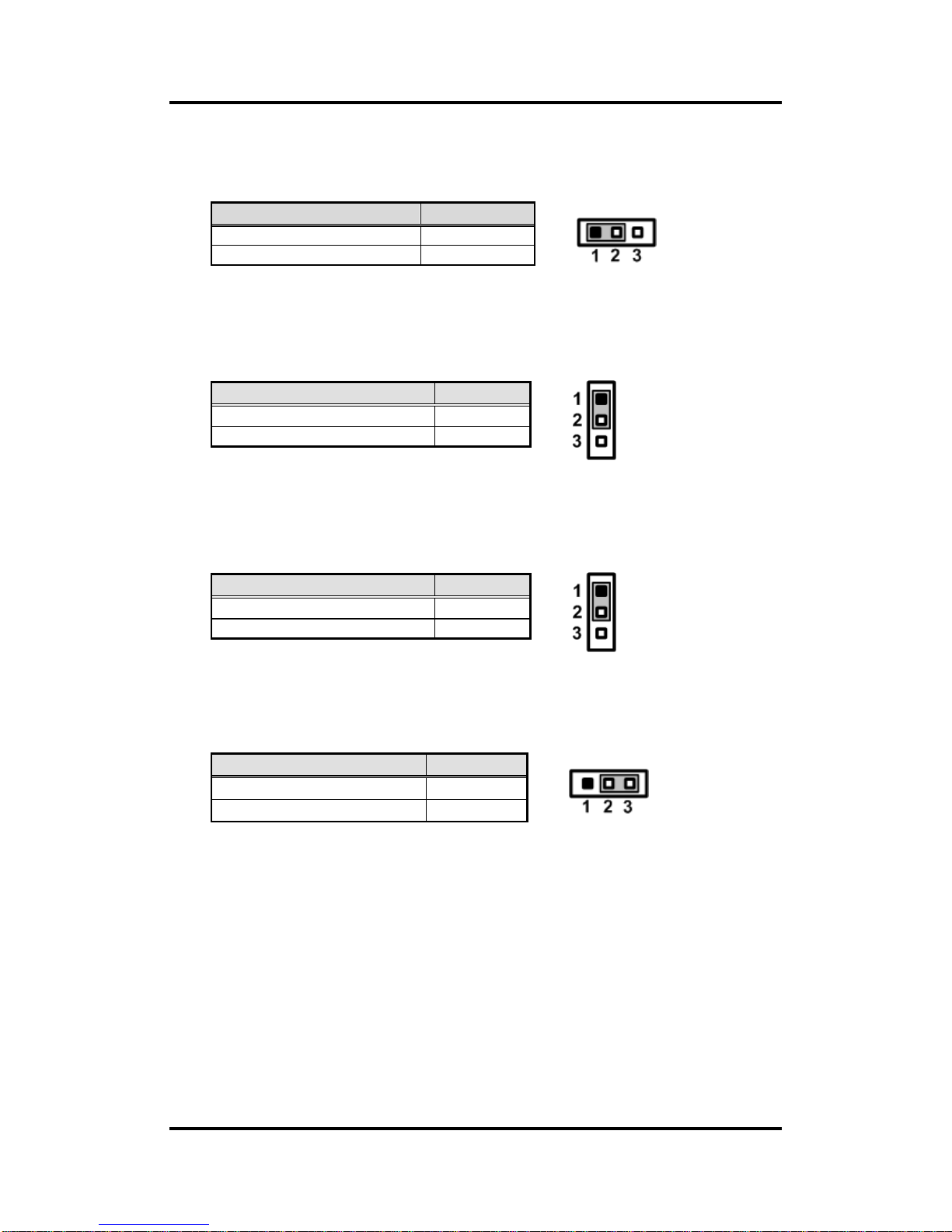
2.4.5 DDR3/3L Voltage Selection (JP5)
This jumper is for DDR3/3L voltage selection. The +1.35V is for DDR3 low voltage
module (DDR3L).
2.4.6 RCC Enable (JP6)
RCC is a Remote Control Controller for DASH function. Use this jumper for updating
RCC firmware via SWIM interface, see section 2.5.8 for CN11.
2.4.7 Restore BIOS Optimal Defaults (JP7)
Put jumper clip to pin 2-3 for a few seconds then move it back to pin 1-2. Doing this
procedure can restore BIOS optimal defaults.
2.4.8 Buzzer Selection (CN1)
Select external or internal buzzer.
Function
Setting
+1.5V (Default)
1-2 close
+1.35V
2-3 close
Function
Setting
Enable (Default)
1-2 close
Disable
2-3 close
Function
Setting
Normal (Default)
1-2 close
Restore BIOS optimal defaults
2-3 close
Function
Setting
External buzzer
1-2 close
Internal buzzer (Default)
2-3 close
Page 21

PICO121 AMD G-Series Embedded SoC Pico-ITX Board
Board and Pin Assignments 15
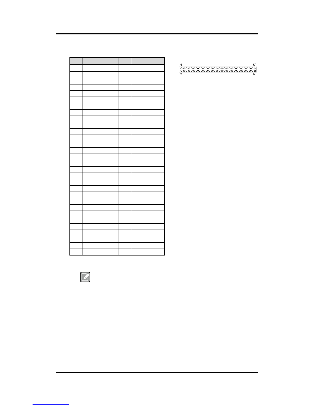
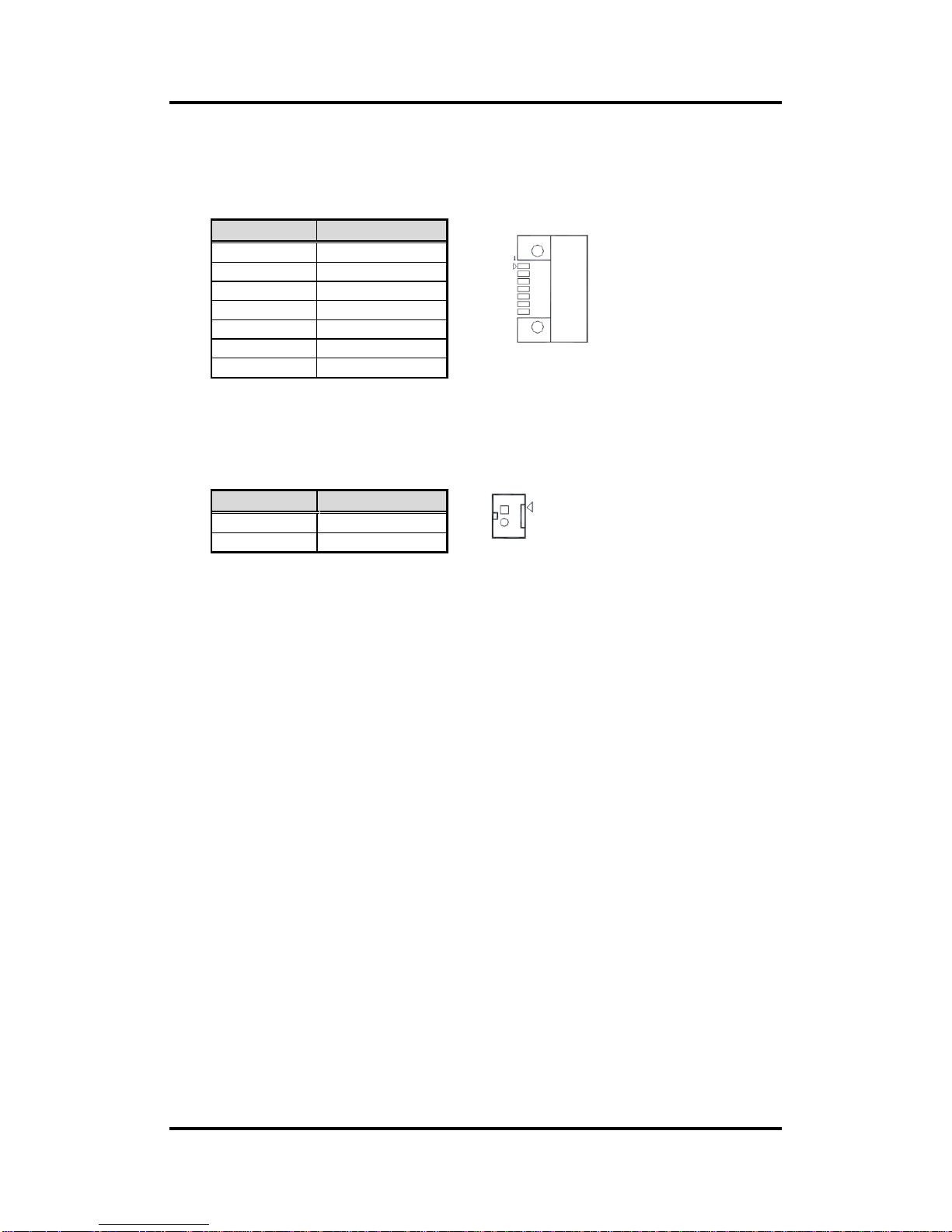
2.5 Connectors
Signals go to other parts of the system through connectors. Loose or improper connection
might cause problems, please make sure all connectors are properly and firmly connected.
Here is a summary table showing connectors on the hardware.
Connector
Description
CN3
Power LED Header
CN4
High Speed Board to Board Connector
CN5
Low Speed Board to Board Connector
CN6
SMBus Connector
CN7
Fan Power Connector
CN8
LVDS Connector
CN9
Serial ATA Power Connector
CN10
Inverter Connector
CN11
SWIM Connector
CN12
DC Power In Connector
CN13
VGA Connector
LAN1
Ethernet Connector
SATA1
Serial ATA Connector
BAT1
CMOS Battery Connector
SCN1
Full-size PCI-Express Mini Card and mSATA Connector
SCN2
SIM Card Slot
SCN3
Half-size PCI-Express Mini Card Connector
SDIMM1
DDR3/3L SO-DIMM Connector
Page 22

PICO121 AMD G-Series Embedded SoC Pico-ITX Board
16 Board and Pin Assignments
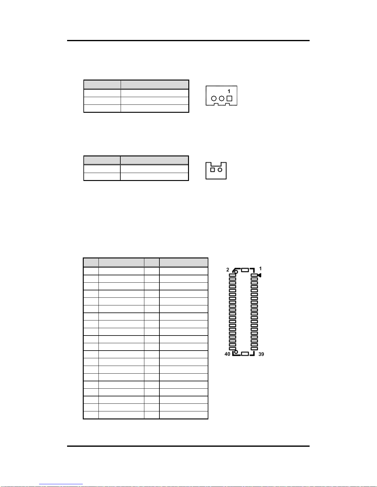
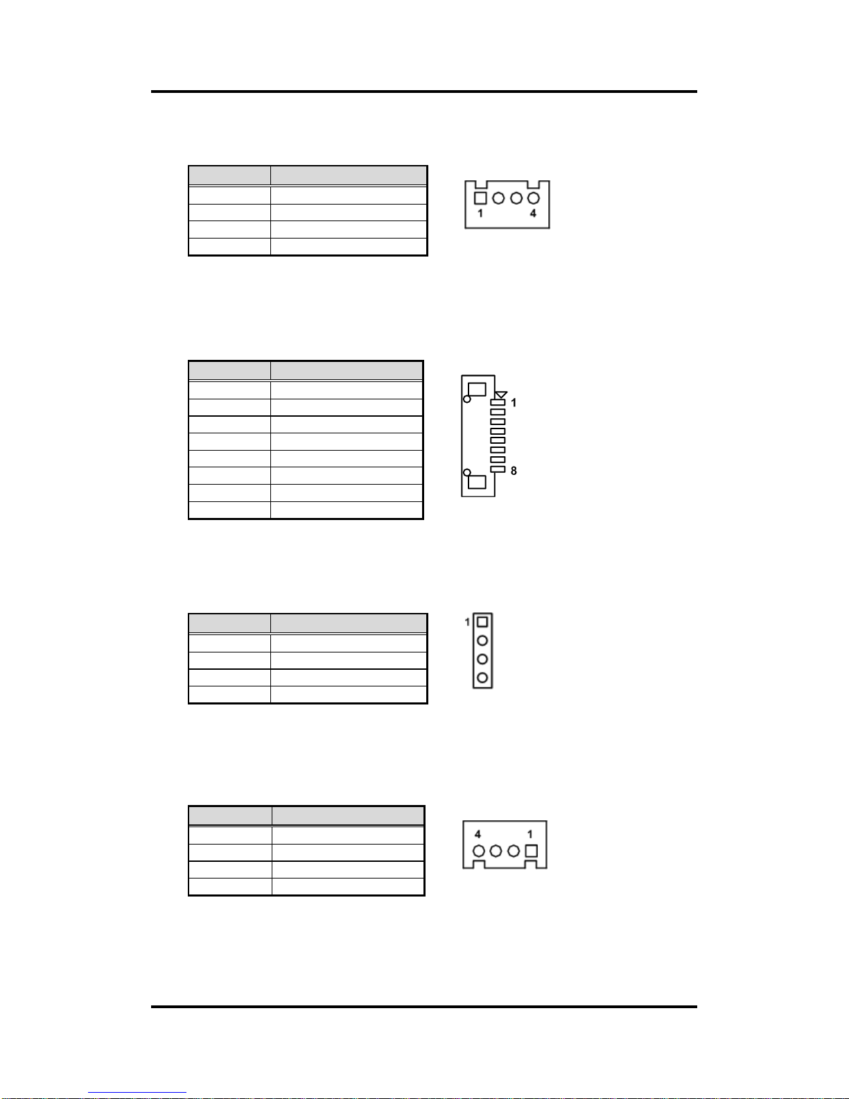
2.5.1 Power LED Header (CN3)
This header is for power LED interface.
2.5.2 High and Low Speed Board to Board Connectors (CN4 and
CN5)
CN4 is a 2x20-pin high speed board to board connector. The pin assignments of CN4
are given as follows.
40 2
39 1
Pin
Signal
1
+5V 2 GND
Pin
Signal
Pin
Signal
1
USB3_TX0_DP
2
DP0_HPD
3
USB3_TX0_DN
4
DP0_AUX_P
5
GND
6
DP0_AUX_N
7
USB3_RX0_DP
8
GND
9
USB3_RX0_DN
10
DP0_TX3_P
11
GND
12
DP0_TX3_N
13
USB3_TX1_DP
14
GND
15
USB3_TX1_DN
16
DP0_TX2_P
17
GND
18
DP0_TX2_N
19
USB3_RX1_DP
20
+5V
21
USB3_RX1_DN
22
DP0_TX1_P
23
GND
24
DP0_TX1_N
25
N/A
26
GND
27
PCIE_TXP2
28
DP0_TX0_P
29
PCIE_TXN2
30
DP0_TX0_N
31
GND
32
GND
33
PCIE_RXP2
34
PCIE_LAN1_CLK_P
35
PCIE_RXN2
36
PCIE_LAN1_CLK_N
37
GND
38
GND
39
PCIE_RST#
40
PCIE_WAKE_UP#
1
Page 23
PICO121 AMD G-Series Embedded SoC Pico-ITX Board
Board and Pin Assignments 17
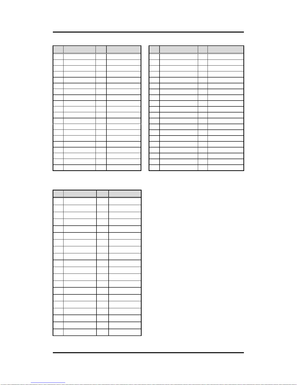
CN5 is a 2x30-pin low speed board to board connector. The pin assignments of CN5 are
given as follows.
Note
It is suggested to insert I/O board (AX93277 or AX93278) into CN4 and
CN5 on PICO121 (see Chapter 3/Appendix A for details of I/O board).
Pin
Signal
Pin
Signal
1
MIC_IN
2
LINE_O_L
3
LINE_IN_L
4
LINE_O_R
5
LINE_IN_R
6
AUDIO_GND
7
AUDIO_GND
8
+5V 9 COMGND
10
+5V
11
DCD1
12
DSR1
13
RXD1
14
RTS1
15
TXD1
16
CTS1
17
DTR1
18
RI1
19
COMGND
20
+5V
21
DCD2
22
DSR2
23
RXD2
24
RTS2
25
TXD2
26
CTS2
27
DTR2
28
RI2
29
GND
30
GND
31
USB_PWR0
32
USB_PWR0
33
C_USB_PN6
34
C_USB_PN7
35
C_USB_PP6
36
C_USB_PP7
37
USB0_GND
38
USB0_GND
39
USB_PWR1
40
USB_PWR1
41
C_USB_PN8
42
C_USB_PN9
43
C_USB_PP8
44
C_USB_PP9
45
USB1_GND
46
USB1_GND
47
+3.3V
48
GND
49
+3.3V
50
GND
51
+3.3V_DUAL
52
FP_PSIN_N
53
+3.3V_DUAL
54
GND
55
HW_RESET_N
56
+5V
57
HDD_ACT#
58
+12V
59
GND
60
+12V
Page 24
PICO121 AMD G-Series Embedded SoC Pico-ITX Board
18 Board and Pin Assignments
2.5.3 SMBus Connector (CN6)
This connector is for SMBus interface. The SMBus (System Management Bus) is a
simple 2-wire bus for the purpose of lightweight communication.
2.5.4 Fan Power Connector (CN7)
This is a 2.5mm pitch wafer connector for fan power interface.
1 2
2.5.5 LVDS Connector (CN8)
This board has a 40-pin connector for LVDS LCD interface. It is strongly recommended
to use the matching JST SHDR-40VS-B 40-pin connector for LVDS interface. Pin 1~6
VCCM can be set to +3.3V, +5V or +12V by setting JP3 or JP1 (see section 2.4.3 or
2.4.1).
18-bit single channel
Pin
Signal
1
SMBus clock
2
SMBus data
3
GND
Pin
Signal
1
+5V 2 GND
Pin
Signal
Pin
Signal
1
VCCM
2
VCCM
3
VCCM
4
VCCM
5
VCCM
6
VCCM
7
N.C 8 N.C 9 GND
10
GND
11
N.C
12
N.C
13
N.C
14
N.C
15
GND
16
GND
17
N.C
18
N.C
19
N.C
20
N.C
21
GND
22
GND
23
Channel A D0-
24
N.C
25
Channel A D0+
26
N.C
27
GND
28
GND
29
Channel A D1-
30
N.C
31
Channel A D1+
32
N.C
33
GND
34
GND
35
Channel A D2-
36
Channel A CLK-
37
Channel A D2+
38
Channel A CLK+
39
GND
40
GND
Page 25
PICO121 AMD G-Series Embedded SoC Pico-ITX Board
Board and Pin Assignments 19
24-bit single channel 18-bit dual channel
24-bit dual channel
Pin
Signal
Pin
Signal
1
VCCM
2
VCCM
3
VCCM
4
VCCM
5
VCCM
6
VCCM
7
N.C 8 N.C
9
GND
10
GND
11
N.C
12
N.C
13
N.C
14
N.C
15
GND
16
GND
17
N.C
18
N.C
19
N.C
20
N.C
21
GND
22
GND
23
Channel A D0-
24
N.C
25
Channel A D0+
26
N.C
27
GND
28
GND
29
Channel A D1-
30
Channel A D3-
31
Channel A D1+
32
Channel A D3+
33
GND
34
GND
35
Channel A D2-
36
Channel A CLK-
37
Channel A D2+
38
Channel A CLK+
39
GND
40
GND
Pin
Signal
Pin
Signal
1
VCCM
2
VCCM
3
VCCM
4
VCCM
5
VCCM
6
VCCM
7
N.C 8 N.C
9
GND
10
GND
11
N.C
12
Channel B D0-
13
N.C
14
Channel B D0+
15
GND
16
GND
17
Channel B CLK-
18
Channel B D1-
19
Channel B CLK+
20
Channel B D1+
21
GND
22
GND
23
Channel A D0-
24
Channel B D2-
25
Channel A D0+
26
Channel B D2+
27
GND
28
GND
29
Channel A D1-
30
N.C
31
Channel A D1+
32
N.C
33
GND
34
GND
35
Channel A D2-
36
Channel A CLK-
37
Channel A D2+
38
Channel A CLK+
39
GND
40
GND
Pin
Signal
Pin
Signal
1
VCCM
2
VCCM
3
VCCM
4
VCCM
5
VCCM
6
VCCM
7
N.C
8
N.C
9
GND
10
GND
11
Channel B D3-
12
Channel B D0-
13
Channel B D3+
14
Channel B D0+
15
GND
16
GND
17
Channel B CLK-
18
Channel B D1-
19
Channel B CLK+
20
Channel B D1+
21
GND
22
GND
23
Channel A D0-
24
Channel B D2-
25
Channel A D0+
26
Channel B D2+
27
GND
28
GND
29
Channel A D1-
30
Channel A D3-
31
Channel A D1+
32
Channel A D3+
33
GND
34
GND
35
Channel A D2-
36
Channel A CLK-
37
Channel A D2+
38
Channel A CLK+
39
GND
40
GND
Page 26
PICO121 AMD G-Series Embedded SoC Pico-ITX Board
20 Board and Pin Assignments
2.5.6 Serial ATA Power Connector (CN9)
This is a 2.0mm pitch wafer connector for Serial ATA (SATA) power interface.
2.5.7 Inverter Connector (CN10)
This is a DF13-8S-1.25C 8-pin connector for inverter. We strongly recommend you to
use the matching DF13-8S-1.25C connector to avoid malfunction.
2.5.8 SWIM Connector (CN11)
This is a 2.0mm pitch pin header for updating RCC firmware.
2.5.9 DC Power In Connector (CN12)
This is a 1x4-pin wafer connector for DC +12V input.
Pin
Signal
1
+12V
2
GND
3
GND
4
+5V
Pin
Signal
1
+12V
2
+12V
3
+5V 4 BL_ENABLE
5
GND
6
GND
7
GND
8
BR_CTRL
Pin
Signal
1
+3.3V
2
SWIM
3
SWIM_RST
4
GND
Pin
Signal
1
+12V
2
+12V
3
GND
4
GND
Page 27
PICO121 AMD G-Series Embedded SoC Pico-ITX Board
Board and Pin Assignments 21
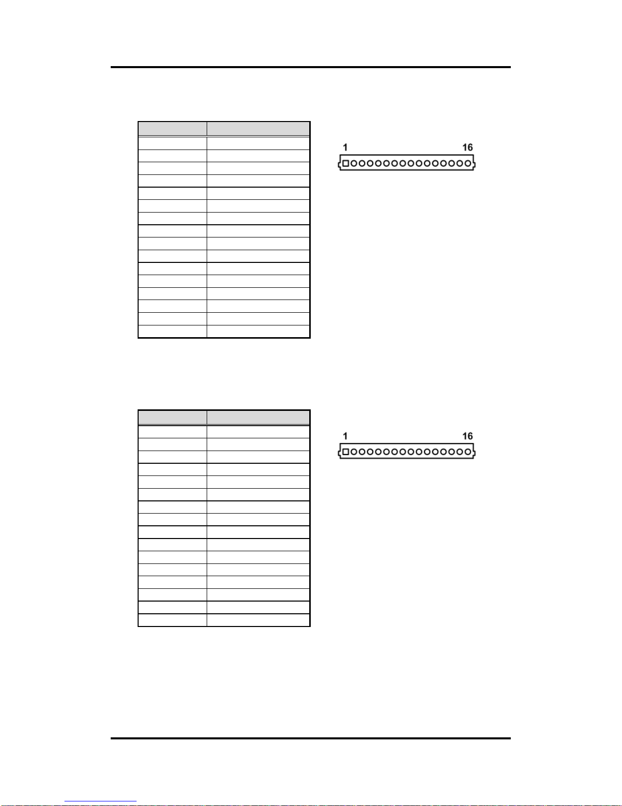
2.5.10 VGA Connector (CN13)
This is a 16-pin wafer connector for VGA interface.
2.5.11 Ethernet Connector (LAN1)
This is a 16-pin wafer connector for Ethernet interface.
Pin
Signal
1
RSVD
2
RED
3
GND
4
GREEN
5
GND
6
BLUE
7
GND
8
VCC
9
DDC_DATA
10
GND
11
GND
12
HSYNC
13
GND
14
VSYNC
15
DDC_CLK
16
GND
Pin
Signal
1
1000 LAN LED
2
100 LAN LED
3
GND
4
MDI3-
5
MDI3+
6
MDI1-
7
MDI2-
8
MDI2+
9
MDI1+
10
MDI0-
11
MDI0+
12
GND
13
LAN_VDD33
14
LAN_LINK_ACT
15
GND
16
GND
Page 28
PICO121 AMD G-Series Embedded SoC Pico-ITX Board
22 Board and Pin Assignments
2.5.12 Serial ATA Connector (SATA1)
This Serial Advanced Technology Attachment (Serial ATA or SATA) connector is for
high-speed SATA interface port. It is a computer bus interface for connecting to devices
such as hard disk drives.
2.5.13 CMOS Battery Connector (BAT1)
This connector is for CMOS battery interface.
Pin
Signal
1
GND
2
TXP 3 TXN 4 GND
5
RXN
6
RXP 7 GND
Pin
Signal
1
+3.3V
2
GND
1 7
1
Page 29
PICO121 AMD G-Series Embedded SoC Pico-ITX Board
Board and Pin Assignments 23
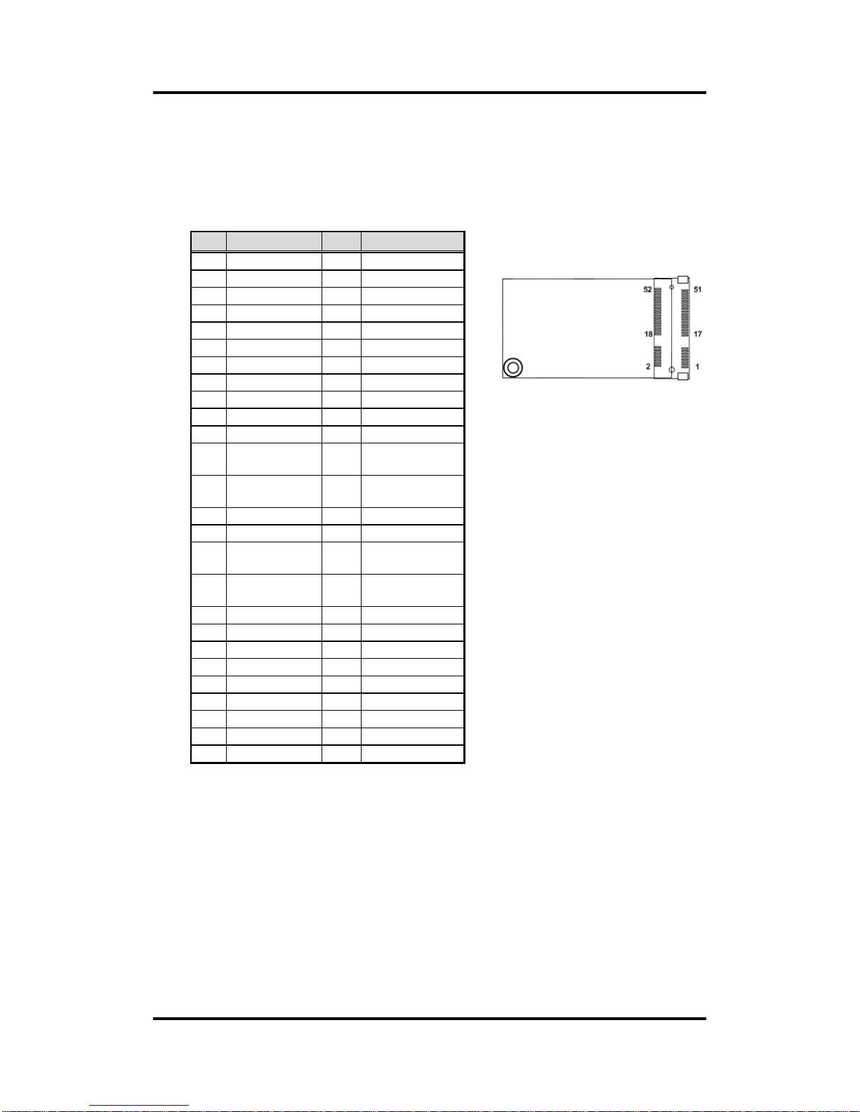
2.5.14 Full-size PCI-Express Mini Card and mSATA Connector
(SCN1)
The SCN1 features full-size PCI-Express Mini Card with mSATA support. It supports the
PCI-Express Mini Cards which are applied to either PCI-Express x1 or USB. It also
complies with PCI-Express Mini Card Spec. V1.2. You are allowed to select PCI-Express
Mini Card or mSATA support via BIOS setting (see section 6.4).
Pin
Signal
Pin
Signal
1
WAKE#
2
+3.3VSB
3
RSVD1
4
GND
5
RSVD2
6
+1.5V
7
CLKREQ#
8
SIM_PWR
9
GND
10
SIM_I/O
11
REFCLK-
12
SIM_CLK
13
REFCLK+
14
SIM_RST
15
GND
16
SIM_VCC
17
RSVD3
18
GND
19
RSVD4
20
RSVD9
21
GND
22
PERST#
23
PE_RXN0/
SATA_RXP1
24
+3.3VSB
25
PE_RXP0/
SATA_RXN1
26
GND
27
GND
28
+1.5V
29
GND
30
SMB_CLK
31
PE_TXN0/
SATA_TXN1
32
SMB_DATA
33
PE_TXP0/
SATA_TXP1
34
GND
35
GND
36
USB_D4-
37
GND
38
USB_D4+
39
+3.3VSB
40
GND
41
+3.3VSB
42
RSVD
43
GND
44
RSVD
45
RSVD5
46
RSVD
47
RSVD6
48
+1.5V
49
RSVD7
50
GND
51
RSVD8
52
+3.3VSB
Page 30
PICO121 AMD G-Series Embedded SoC Pico-ITX Board
24 Board and Pin Assignments
2.5.15 SIM Card Slot (SCN2)
The SCN2 is for inserting SIM Card. It is mainly used in 3G wireless network application.
In order to work properly, the SIM Card must be used together with 3G module which is
inserted to SCN1 or SCN3.
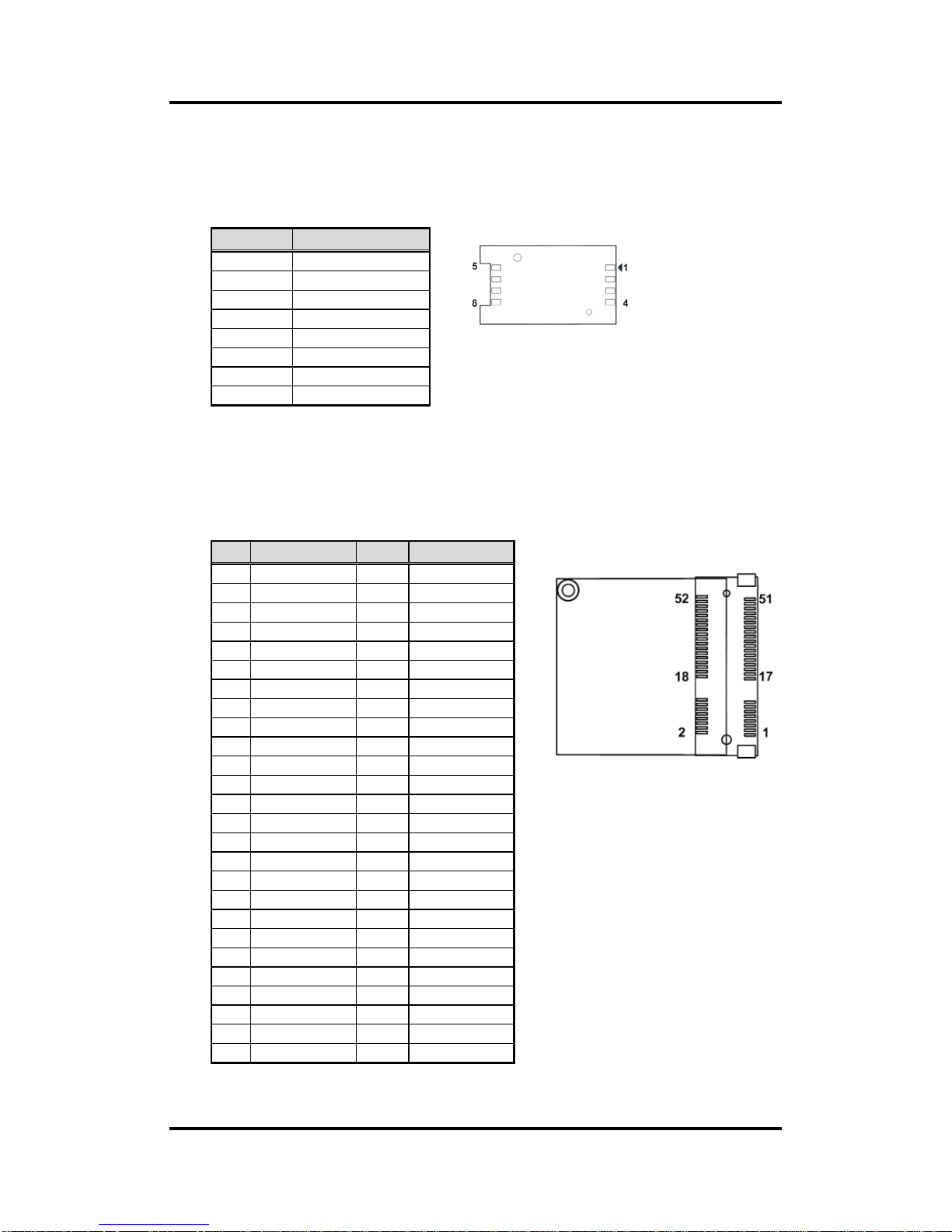
2.5.16 Half-size PCI-Express Mini Card Connector (SCN3)
The SCN3 is a half-size PCI-Express Mini Card connector. It supports the PCI-Express
Mini Cards which are applied to either PCI-Express x1 or USB. It complies with
PCI-Express Mini Card Spec. V1.2.
Pin
Signal
1
PWR
2
RST 3 CLK 4 NC 5 GND
6
VPP 7 I/O 8 NC
Pin
Signal
Pin
Signal
1
WAKE#
2
+3.3VSB
3
RSVD1
4
GND
5
RSVD2
6
+1.5V
7
CLKREQ#
8
SIM_PWR
9
GND
10
SIM_I/O
11
REFCLK-
12
SIM_CLK
13
REFCLK+
14
SIM_RST
15
GND
16
SIM_VCC
17
RSVD3
18
GND
19
RSVD4
20
RSVD9
21
GND
22
PERST#
23
PE_RXN1
24
+3.3VSB
25
PE_RXP1
26
GND
27
GND
28
+1.5V
29
GND
30
SMB_CLK
31
PE_TXN1
32
SMB_DATA
33
PE_TXP1
34
GND
35
GND
36
USB_D5-
37
GND
38
USB_D5+
39
+3.3VSB
40
GND
41
+3.3VSB
42
RSVD
43
GND
44
RSVD
45
RSVD5
46
RSVD
47
RSVD6
48
+1.5V
49
RSVD7
50
GND
51
RSVD8
52
+3.3VSB
Page 31

PICO121 AMD G-Series Embedded SoC Pico-ITX Board
AX93277 I/O Board 25
Chapter 3
AX93277 I/O Board
The AX93277 is an I/O expansion board which is suggested to insert carefully into CN4 and
CN5 on PICO121. Its specifications and detailed information are given in this chapter.
3.1 AX93277 Specifications
Size
118mm x 29mm
Features
Support audio jack (MIC-in/line-out).
Four USB 2.0.
Serial Ports: One port for RS-232/422/485 and one port for RS-232.
Power-on, reset and red/green LED.
Note
All specifications and images are subject to change without notice.
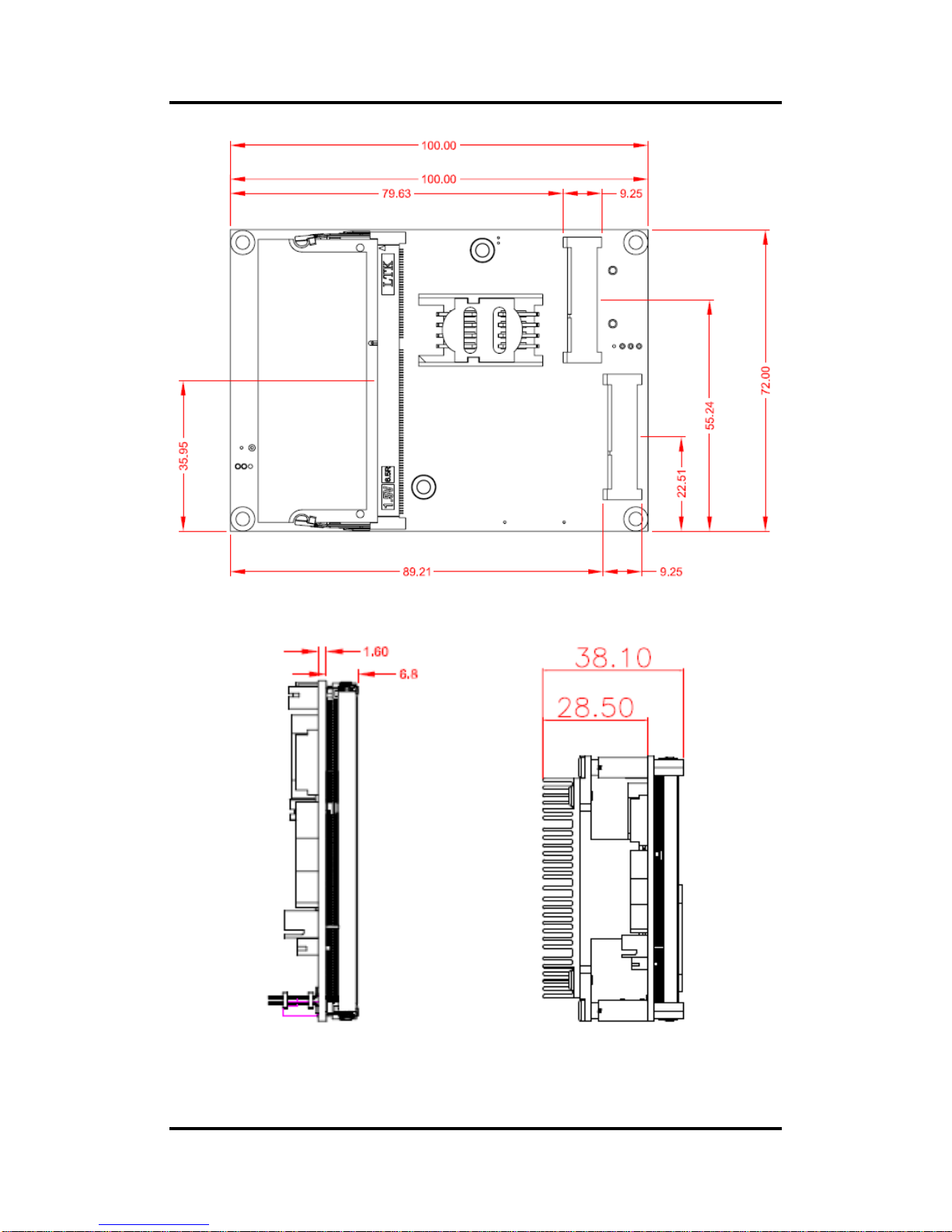
3.2 AX93277 Dimensions and Fixing Holes
Top View
Page 32

PICO121 AMD G-Series Embedded SoC Pico-ITX Board
26 AX93277 I/O Board
Bottom View
Side View
Page 33

PICO121 AMD G-Series Embedded SoC Pico-ITX Board
AX93277 I/O Board 27
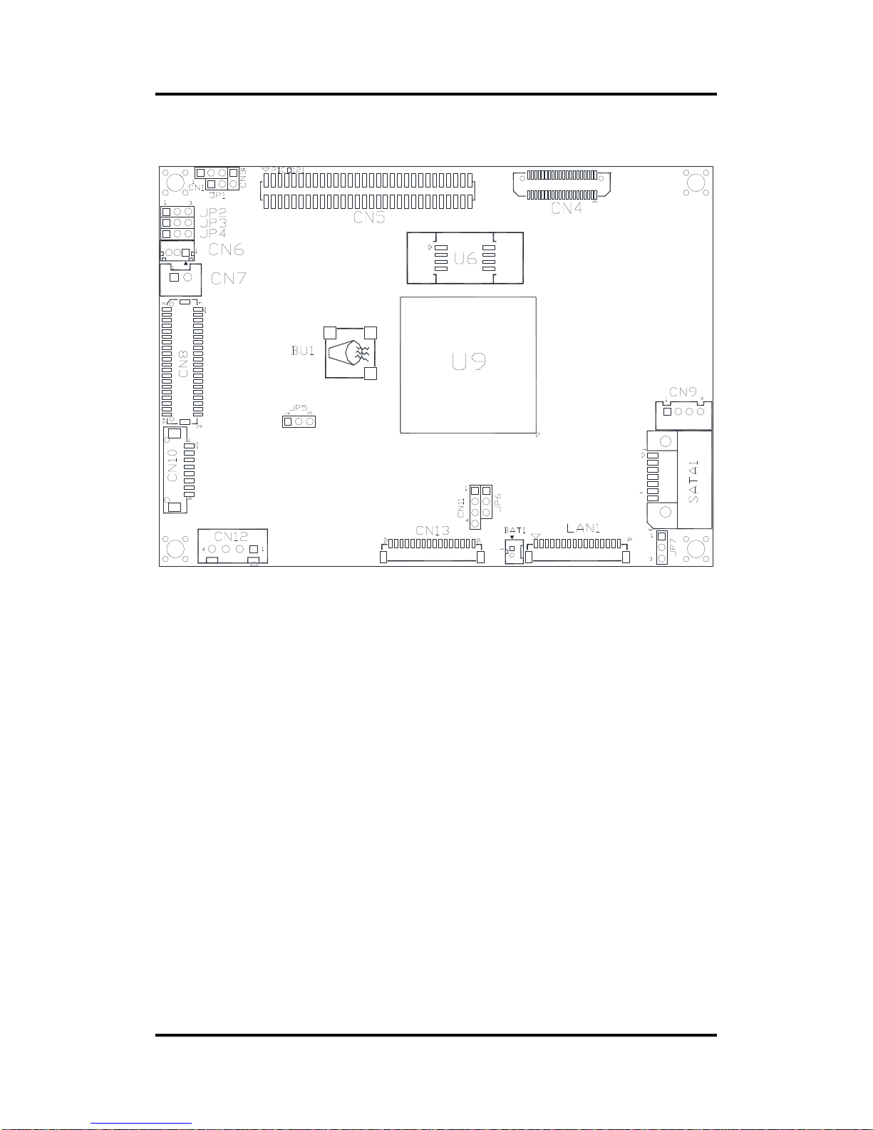
3.3 AX93277 Board Layout
Top View
Side View
Page 34

PICO121 AMD G-Series Embedded SoC Pico-ITX Board
28 AX93277 I/O Board
3.4 AX93277 Jumper Settings
Properly configure jumper settings on the AX93277 I/O board to meet your application purpose.
Below you can find a summary table of all jumpers and onboard default settings.
Note
Once the default jumper setting needs to be changed, please do it under power-off
condition.
Jumper
Description
Setting
JP1
COM1 Data/+12V Power Selection
Default: RS-232 Data
CN6 Pin 18: RI
1-2 Close
JP2
COM1 Data/+5V Power Selection
Default: RS-232 Data
CN6 Pin 10: DCD
1-2 Close
3.4.1 COM1 Data/Power Selection (JP1 and JP2)
The COM1 port has +12V level power capability on RI and +5V level on DCD by setting
JP1 and JP2, respectively. When this port is set to +12V or +5V level, please make sure
its communication mode is RS-232 (see BIOS setting in section 6.4).
Function
JP1 Setting
Data: Set CN6 pin 18 to RI (Default)
1-2 close
Power: Set CN6 pin 18 to +12V level
2-3 close
Function
JP2 Setting
Data: Set CN6 pin 10 to DCD (Default)
1-2 close
Power: Set CN6 pin 10 to +5V level
2-3 close
Page 35

PICO121 AMD G-Series Embedded SoC Pico-ITX Board
AX93277 I/O Board 29
3.5 AX93277 Connectors, Switches and LED
Signals go to other parts of the system through connectors. Loose or improper connection
might cause problems, please make sure all connectors are properly and firmly connected.
Here is a summary table which shows connectors, switches and LED on the hardware.
Connector
Description
CN2
High Speed Board to Board Connector
CN5
System Power Switch
CN6
COM Connector
CN8
Audio Jack
CN9
System Reset Switch
CN10
Low Speed Board to Board Connector
USB1~USB2
USB 2.0 Connectors
D1
Power and HDD LED Indicator
3.5.1 High and Low Speed Board to Board Connectors (CN2 and
CN10)
CN2 is a 2x20-pin high speed board to board connector. The pin assignments of CN2
are given as follows.
40 2
39 1
Pin
Signal
Pin
Signal
1
USB3_TX0_DP
2
DP0_HPD
3
USB3_TX0_DN
4
DP0_AUX_P
5
GND
6
DP0_AUX_N
7
USB3_RX0_DP
8
GND
9
USB3_RX0_DN
10
DP0_TX3_P
11
GND
12
DP0_TX3_N
13
USB3_TX1_DP
14
GND
15
USB3_TX1_DN
16
DP0_TX2_P
17
GND
18
DP0_TX2_N
19
USB3_RX1_DP
20
+5V
21
USB3_RX1_DN
22
DP0_TX1_P
23
GND
24
DP0_TX1_N
25
N/A
26
GND
27
PCIE_TXP2
28
DP0_TX0_P
29
PCIE_TXN2
30
DP0_TX0_N
31
GND
32
GND
33
PCIE_RXP2
34
PCIE_LAN1_CLK_P
35
PCIE_RXN2
36
PCIE_LAN1_CLK_N
37
GND
38
GND
39
PCIE_RST#
40
PCIE_WAKE_UP#
Page 36

PICO121 AMD G-Series Embedded SoC Pico-ITX Board
30 AX93277 I/O Board
CN10 is a 2x30-pin low speed board to board connector. The pin assignments of CN10
are given as follows.
Note
Please gently insert CN2 and CN10 into CN4 and CN5 on PICO121.
Pin
Signal
Pin
Signal
1
MIC_IN
2
LINE_O_L
3
LINE_IN_L
4
LINE_O_R
5
LINE_IN_R
6
AUDIO_GND
7
AUDIO_GND
8
+5V 9 COMGND
10
+5V
11
DCD1
12
DSR1
13
RXD1
14
RTS1
15
TXD1
16
CTS1
17
DTR1
18
RI1
19
COMGND
20
+5V
21
DCD2
22
DSR2
23
RXD2
24
RTS2
25
TXD2
26
CTS2
27
DTR2
28
RI2
29
GND
30
GND
31
USB_PWR0
32
USB_PWR0
33
C_USB_PN6
34
C_USB_PN7
35
C_USB_PP6
36
C_USB_PP7
37
USB0_GND
38
USB0_GND
39
USB_PWR1
40
USB_PWR1
41
C_USB_PN8
42
C_USB_PN9
43
C_USB_PP8
44
C_USB_PP9
45
USB1_GND
46
USB1_GND
47
+3.3V
48
GND
49
+3.3V
50
GND
51
+3.3V_DUAL
52
FP_PSIN_N
53
+3.3V_DUAL
54
GND
55
HW_RESET_N
56
+5V
57
HDD_ACT#
58
+12V
59
GND
60
+12V
Page 37

PICO121 AMD G-Series Embedded SoC Pico-ITX Board
AX93277 I/O Board 31
COM1
COM2
3.5.2 System Power Switch (CN5)
This switch is for turning on/off the system power.
3.5.3 COM Connector (CN6)
CN6 is a double-deck DB-9 connector for COM1 (lower) and COM2 (upper). COM1
comes with power capability on DCD and RI pins by setting jumpers (see section 3.4.1).
The pin assignments of RS-232/RS-422/RS-485 are listed in table below. If you need
COM1 port to support RS-422 or RS-485, please refer to BIOS setting in section 6.4.
COM1:
COM2:
3.5.4 Audio Jack (CN8)
This is audio jack with HD audio support. Install audio driver, and then attach audio
devices to CN8.
Function
Description
On
Turn on/off system
Off
Keep system status
Pin
RS-232
RS-422
RS-485
10
DCD
TX-
Data-
11
RXD
TX+
Data+
12
TXD
RX+
N.C
13
DTR
RX-
N.C.
14
GND
No use
No use
15
DSR
No use
No use
16
RTS
No use
No use
17
CTS
No use
No use
18
RI
No use
No use
Pin
Signal
1
DCD
2
RXD
3
TXD 4 DTR 5 GND
6
DSR
7
RTS 8 CTS 9 RI
Pin Color
Signal
Green
Line-out
Pink
MIC-in
Page 38

PICO121 AMD G-Series Embedded SoC Pico-ITX Board
32 AX93277 I/O Board
3.5.5 System Reset Switch (CN9)
This switch reboots your computer without turning off the power supply. It is a better way
to reboot your system for a longer life of the system power supply.
3.5.6 USB 2.0 Connectors (USB1 and USB2)
The board comes with two double-deck Universal Serial Bus (compliant with USB 2.0
(480Mbps)) connectors on the rear I/O for installing USB peripherals such as keyboard,
mouse, scanner, etc.
1 2 3 4
5 6 7 8
3.5.7 Power and HDD LED Indicator (D1)
The red LED is linked to Hard Disk Drive (HDD) activity signal. LED flashes every time
HDD is accessed.
The power LED (green) lights up and will remain steady while the system is powered on.
Function
Description
On
Reset system
Off
Keep system status
Pin
Signal
Pin
Signal
1
+5V 5 +5V 2 USB1/3_DATA-
6
USB2/4_DATA-
3
USB1/3_DATA+
7
USB2/4_DATA+
4
GND
8
GND
LED Color
Description
Red
Hard disk drive activity
Green
Power on/off
Page 39

PICO121 AMD G-Series Embedded SoC Pico-ITX Board
AX93267 I/O Board 33
Chapter 4
AX93267 I/O Board
The AX93267 is an I/O expansion board which is suggested to connect to PICO121. Its
specifications and detailed information are given in this chapter.
4.1 AX93267 Specifications
Size
29.25mm x 118mm
Features
One D-Sub VGA port
One RJ-45 Ethernet port.
DC power jack.
Note: All specifications and images are subject to change without notice.
Page 40

PICO121 AMD G-Series Embedded SoC Pico-ITX Board
34 AX93267 I/O Board
4.2 AX93267 Dimensions and Fixing Holes
Top View
Side View
Page 41

PICO121 AMD G-Series Embedded SoC Pico-ITX Board
AX93267 I/O Board 35
4.3 AX93267 Board Layout
Top View
Side View
Page 42

PICO121 AMD G-Series Embedded SoC Pico-ITX Board
36 AX93267 I/O Board
4.4 AX93267 Connectors
Signals go to other parts of the system through connectors. Loose or improper connection
might cause problems, please make sure all connectors are properly and firmly connected.
Here is a summary table which shows all connectors on the hardware.
Connector
Description
CN1
DC Power Jack
CN2
DC Power In Connector
CN3
VGA Connector
CN4
D-Sub VGA Connector
CN5
Ethernet Connector
CN6
RJ-45 Ethernet Port
4.4.1 DC Power Jack (CN1)
The CN1 is a DC power jack for DC +12V input.
4.4.2 DC Power In Connector (CN2)
This is a 1x4-pin wafer connector for DC +12V input. It is suggested to connect this CN2
to PICO121’s CN12.
Pin
Signal
1
GND
2
GND
3
+12V
4
+12V
Pin
Signal
1
+12V
2
+12V
3
GND
4
GND
Page 43

PICO121 AMD G-Series Embedded SoC Pico-ITX Board
AX93267 I/O Board 37
4.4.3 VGA Connector (CN3)
This is a 16-pin wafer connector for VGA interface. Gently connect this CN3 to
PICO121’s CN13.
4.4.4 D-Sub VGA Connector (CN4)
The CN4 is a standard 15-pin D-Sub connector. It is commonly used for VGA display.
This VGA interface configuration can be configured via software utility.
Pin
Signal
1
RSVD
2
RED
3
GND
4
GREEN
5
GND
6
BLUE
7
GND
8
VCC
9
DDC_DATA
10
GND
11
GND
12
HSYNC
13
GND
14
VSYNC
15
DDC_CLK
16
GND
Pin
Signal
Pin
Signal
1
RED
2
GREEN
3
BLUE
4
N.C 5 GND
6
CRT_DETE
7
GND
8
GND
9
CRT_VCC
10
GND
11
N.C
12
DDC_DATA
13
Hsync
14
Vsync
15
DDC_CLK
Page 44

PICO121 AMD G-Series Embedded SoC Pico-ITX Board
38 AX93267 I/O Board
4.4.5 Ethernet Connector (CN5)
This is a 16-pin wafer connector for Ethernet interface. Gently connect this CN5 to
PICO121’s LAN1.
4.4.6 RJ-45 Ethernet Port (CN6)
This board has one RJ-45 Ethernet connector. Connection can be established by
plugging one end of the Ethernet cable into this RJ-45 connector and the other end
(phone jack) to a 1000/100/10-Base-T hub.
Pin
Signal
1
1000 LAN LED
2
100 LAN LED
3
GND
4
MDI3-
5
MDI3+
6
MDI1-
7
MDI2-
8
MDI2+
9
MDI1+
10
MDI0-
11
MDI0+
12
GND
13
LAN_VDD33
14
LAN_LINK_ACT
15
GND
16
GND
Pin
Signal
Pin
Signal
L1
MDI0P
L5
MDI2P
L2
MDI0N
L6
MDI2N
L3
MDI1P
L7
MDI3P
L4
MDI1N
L8
MDI3N
A
Active LED (Yellow)
B
100 LAN LED (Green) / 1000 LAN LED
(Orange)
Page 45

PICO121 AMD G-Series Embedded SoC Pico-ITX Board
Hardware Description 39
Chapter 5
Hardware Description
5.1 Microprocessors
The PICO121 supports AMD G-Series Embedded SoC GX-210HA/GX-210JA processors,
which enable your system to operate under Windows® 7 and Windows® 8 environments. The
system performance depends on the microprocessor. Make sure all correct settings are
arranged for your installed microprocessor to prevent the CPU from damages.
5.2 BIOS
The PICO121 uses AMI Plug and Play BIOS with a single 16Mbit SPI Flash.
5.3 System Memory
The PICO121 supports one 204-pin DDR3/3L SO-DIMM socket for a maximum memory of
8GB DDR3/3L SDRAMs. The memory module comes in sizes of 1GB, 2GB, 4GB and 8GB.
Page 46

PICO121 AMD G-Series Embedded SoC Pico-ITX Board
40 Hardware Description
5.4 I/O Port Address Map
The AMD G-Series Embedded SoC GX-210HA/GX-210JA processors communicate via I/O
ports. Total 1KB port addresses are available for assigning to other devices via I/O expansion
cards.
Page 47

PICO121 AMD G-Series Embedded SoC Pico-ITX Board
Hardware Description 41
Page 48

PICO121 AMD G-Series Embedded SoC Pico-ITX Board
42 Hardware Description
5.5 Interrupt Controller (IRQ) Map
The interrupt controller (IRQ) mapping list is shown as follows:
Page 49

PICO121 AMD G-Series Embedded SoC Pico-ITX Board
Hardware Description 43
Page 50

PICO121 AMD G-Series Embedded SoC Pico-ITX Board
44 Hardware Description
Page 51

PICO121 AMD G-Series Embedded SoC Pico-ITX Board
Hardware Description 45
5.6 Memory Map
The memory mapping list is shown as follows:
Page 52

PICO121 AMD G-Series Embedded SoC Pico-ITX Board
46 Hardware Description
This page is intentionally left blank.
Page 53

PICO121 AMD G-Series Embedded SoC Pico-ITX Board
AMI BIOS Setup Utility 47
Chapter 6
AMI BIOS Setup Utility
The AMI UEFI BIOS provides users with a built-in setup program to modify basic system
configuration. All configured parameters are stored in a flash chip to save the setup information
whenever the power is turned off. This chapter provides users with detailed description about
how to set up basic system configuration through the AMI BIOS setup utility.
6.1 Starting
To enter the setup screens, follow the steps below:
1. Turn on the computer and press the <Del> key immediately.
2. After you press the <Del> key, the main BIOS setup menu displays. You can access the
other setup screens from the main BIOS setup menu, such as the Advanced and Chipset
menus.
Note
If your computer cannot boot after making and saving system changes with BIOS
setup, you can restore BIOS optimal defaults by setting JP7 (see section 2.4.7).
It is strongly recommended that you should avoid changing the chipset’s defaults. Both AMI
and your system manufacturer have carefully set up these defaults that provide the best
performance and reliability.
6.2 Navigation Keys
The BIOS setup/utility uses a key-based navigation system called hot keys. Most of the BIOS
setup utility hot keys can be used at any time during the setup navigation process. These keys
include <F1>, <F2>, <Enter>, <ESC>, <Arrow> keys, and so on.
Note
Some of the navigation keys differ from one screen to another .
Page 54

PICO121 AMD G-Series Embedded SoC Pico-ITX Board
48 AMI BIOS Setup Utility
Hot Keys
Description
Left/Right
The Left and Right <Arrow> keys allow you to select a setup screen.
Up/Down
The Up and Down <Arrow> keys allow you to select a setup screen or
sub-screen.
+ Plus/Minus
The Plus and Minus <Arrow> keys allow you to change the field value of a
particular setup item.
Tab
The <Tab> key allows you to select setup fields.
F1
The <F1> key allows you to display the General Help screen.
F2
The <F2> key allows you to Load Previous Values.
F3
The <F3> key allows you to Load Optimized Defaults.
F4
The <F4> key allows you to save any changes you have made and exit
Setup. Press the <F4> key to save your changes.
Esc
The <Esc> key allows you to discard any changes you have made and exit
the Setup. Press the <Esc> key to exit the setup without saving your
changes.
Enter
The <Enter> key allows you to display or change the setup option listed for a
particular setup item. The <Enter> key can also allow you to display the
setup sub- screens.
Page 55

PICO121 AMD G-Series Embedded SoC Pico-ITX Board
AMI BIOS Setup Utility 49
6.3 Main Menu
When you first enter the setup utility, you will enter the Main setup screen. You can always
return to the Main setup screen by selecting the Main tab. System Time/Date can be set up as
described below. The Main BIOS setup screen is shown below.
BIOS/Memory Information
Display the auto-detected BIOS/memory information.
System Language
Choose the system default language.
System Date/Time
Use this option to change the system time and date. Highlight System Time or System
Date using the <Arrow> keys. Enter new values through the keyboard. Press the <Tab>
key or the <Arrow> keys to move between fields. The date must be entered in MM/DD/YY
format. The time is entered in HH:MM:SS format.
Access Level
Display the access level of current user.
Page 56

PICO121 AMD G-Series Embedded SoC Pico-ITX Board
50 AMI BIOS Setup Utility
6.4 Advanced Menu
The Advanced menu also allows users to set configuration of the CPU and other system
devices. You can select any of the items in the left frame of the screen to go to the sub menus:
► ACPI Settings
► CPU Configuration
► IDE Configuration
► USB Configuration
► F81801 Super IO Configuration
► F81801 H/W Monitor
► DASH Setting
For items marked with “”, please press <Enter> for more options.
Page 57

PICO121 AMD G-Series Embedded SoC Pico-ITX Board
AMI BIOS Setup Utility 51
ACPI Settings
ACPI Sleep State
When the suspend button is pressed, the Advanced Configuration and Power Interface
(ACPI) sleep state is S3 only (Suspend to RAM).
Page 58

PICO121 AMD G-Series Embedded SoC Pico-ITX Board
52 AMI BIOS Setup Utility
CPU Configuration
This screen shows the CPU Configuration.
SVM Mode
Enable or disable CPU virtualization (SVM).
Page 59

PICO121 AMD G-Series Embedded SoC Pico-ITX Board
AMI BIOS Setup Utility 53
IDE Configuration
In the IDE Configuration menu, you can see the currently installed hardware in the SATA
ports. During system boot up, the BIOS automatically detects the presence of SATA
devices.
USB Configuration
USB Devices
Display all detected USB devices.
Page 60

PICO121 AMD G-Series Embedded SoC Pico-ITX Board
54 AMI BIOS Setup Utility
F81801 Super IO Configuration
You can use this screen to select options for the Super IO Configuration, and change the
value of the selected option. A description of the selected item appears on the right side of
the screen. For items marked with “”, please press <Enter> for more options.
Serial Port 1 (COM1)/Serial Port 2 (COM2)
Set parameters of serial port 1 (COM1)/serial port 2 (COM2).
Page 61

PICO121 AMD G-Series Embedded SoC Pico-ITX Board
AMI BIOS Setup Utility 55
Serial Port 1 (COM1)
Serial Port
Enable or disable serial port 1. The optimal setting for base I/O address is 3F8h and for
interrupt request address is IRQ4.
COM Mode
Use this option to set RS-232/RS-422/RS-485 communication mode for serial port 1.
Page 62

PICO121 AMD G-Series Embedded SoC Pico-ITX Board
56 AMI BIOS Setup Utility
Serial Port 2 (COM2)
Serial Port
Enable or disable serial port 2. The optimal setting for base I/O address is 2F8h and for
interrupt request address is IRQ3.
Page 63

PICO121 AMD G-Series Embedded SoC Pico-ITX Board
AMI BIOS Setup Utility 57
F81801 H/W Monitor
This screen monitors hardware health status.
This screen displays the temperature of system and CPU, and also system voltages
(VCore and 5V).
Page 64

PICO121 AMD G-Series Embedded SoC Pico-ITX Board
58 AMI BIOS Setup Utility
DASH Setting
You can use this screen to select options for the Desktop Architecture for System
Hardware (DASH) providing the capability to remotely change BIOS settings. Further
information about how to use the DASH can be found in Chapter 8.
ASF Support
Enable or disable Alert Specification Format (ASF) support.
MCTP Support
Enable or disable Management Component Transport Protocol (MCTP) support.
Console Redirection
Enable or disable console redirection for Windows Emergency Management Services
(EMS).
Console Redirection Settings
Display console redirection settings screen.
Page 65

PICO121 AMD G-Series Embedded SoC Pico-ITX Board
AMI BIOS Setup Utility 59
Console Redirection Settings
You can use this screen to set parameters for console redirection settings. Further
information about how to use the DASH can be found in Chapter 8.
Page 66

PICO121 AMD G-Series Embedded SoC Pico-ITX Board
60 AMI BIOS Setup Utility
6.5 Chipset Menu
The Chipset menu allows users to change the advanced chipset settings. You can select any
of the items in the left frame of the screen to go to the sub menus:
► GFX Configuration
► South Bridge
► North Bridge
For items marked with “”, please press <Enter> for more options.
Page 67

PICO121 AMD G-Series Embedded SoC Pico-ITX Board
AMI BIOS Setup Utility 61
GFX Configuration
This screen is for GFX configuration.
Display Port 0 Output Mode
Choose display port 0 output mode. The default is Disabled. Once AX93278 is installed,
please choose HDMI (refer to Appendix A for AX93278 related information).
Display Port 1 Output Mode
Choose display port 1 output mode. The default is LVDS.
LVDS Panel Type
Set LVDS panel by selecting the appropriate setup item.
LVDS Brightness
Select the brightness of LVDS panel ranging from 30% to 100%. The default setting is
70%.
Page 68

PICO121 AMD G-Series Embedded SoC Pico-ITX Board
62 AMI BIOS Setup Utility
South Bridge
This screen allows users to configure parameters of South Bridge chipset.
OnChip SATA Type
Configuration options are Native IDE and AHCI.
Select Mini Card / mSATA Device
This setting is for SCN1 (see section 2.5.14). The default is mSATA. If PCI-Express Mini
Card in PCI-Express x1 link is needed to insert to SCN1, please change setting to Mini
Card.
HD Audio Azalia Device
Control detection of the HD Audio device. Configuration options are Disabled and
Enabled.
Page 69

PICO121 AMD G-Series Embedded SoC Pico-ITX Board
AMI BIOS Setup Utility 63
North Bridge Configuration
This screen shows the North Bridge configuration related information.
Page 70

PICO121 AMD G-Series Embedded SoC Pico-ITX Board
64 AMI BIOS Setup Utility
6.6 Boot Menu
The Boot menu allows users to change boot options of the system.
Setup Prompt Timeout
Number of seconds to wait for setup activation key. 65535(0xFFFF) means indefinite
waiting.
Bootup NumLock State
Use this item to select the power-on state for the keyboard NumLock.
Quiet Boot
Select to display either POST output messages or a splash screen during boot-up.
Launch PXE OpROM policy
Control the execution of UEFI and legacy PXE OpROM.
Boot Option Priorities
These are settings for boot priority. Specify the boot device priority sequence from the
available devices.
Page 71

PICO121 AMD G-Series Embedded SoC Pico-ITX Board
AMI BIOS Setup Utility 65
6.7 Security Menu
The Security menu allows users to change the security settings for the system.
Administrator Password
This item indicates whether an administrator password has been set (installed or
uninstalled).
User Password
This item indicates whether an user password has been set (installed or uninstalled).
Page 72

PICO121 AMD G-Series Embedded SoC Pico-ITX Board
66 AMI BIOS Setup Utility
6.8 Save & Exit Menu
The Save & Exit menu allows users to load your system configuration with optimal or fail-safe
default values.
Save Changes and Exit
When you have completed the system configuration changes, select this option to leave
Setup and return to Main Menu. Select Save Changes and Exit from the Save & Exit menu
and press <Enter>. Select Yes to save changes and exit.
Discard Changes and Exit
Select this option to quit Setup without making any permanent changes to the system
configuration and return to Main Menu. Select Discard Changes and Exit from the Save &
Exit menu and press <Enter>. Select Yes to discard changes and exit.
Save Changes and Reset
When you have completed the system configuration changes, select this option to leave
Setup and reboot the computer so the new system configuration parameters can take
effect. Select Save Changes and Reset from the Save & Exit menu and press <Enter>.
Select Yes to save changes and reset.
Discard Changes and Reset
Select this option to quit Setup without making any permanent changes to the system
configuration and reboot the computer. Select Discard Changes and Reset from the Save
& Exit menu and press <Enter>. Select Yes to discard changes and reset.
Save Changes
When you have completed the system configuration changes, select this option to save
changes. Select Save Changes from the Save & Exit menu and press <Enter>. Select Yes
to save changes.
Page 73

PICO121 AMD G-Series Embedded SoC Pico-ITX Board
AMI BIOS Setup Utility 67
Discard Changes
Select this option to quit Setup without making any permanent changes to the system
configuration. Select Discard Changes from the Save & Exit menu and press <Enter>.
Select Yes to discard changes.
Restore Defaults
It automatically sets all Setup options to a complete set of default settings when you select
this option. Select Restore Defaults from the Save & Exit menu and press <Enter>.
Save as User Defaults
Select this option to save system configuration changes done so far as User Defaults.
Select Save as User Defaults from the Save & Exit menu and press <Enter>.
Restore User Defaults
It automatically sets all Setup options to a complete set of User Defaults when you select
this option. Select Restore User Defaults from the Save & Exit menu and press <Enter>.
Boot Override
Select a drive to immediately boot that device regardless of the current boot order.
Launch EFI Shell from filesystem device
Attempt to launch EFI Shell application (Shellx64.efi) from one of the available filesystem
devices.
Page 74

PICO121 AMD G-Series Embedded SoC Pico-ITX Board
68 AMI BIOS Setup Utility
This page is intentionally left blank.
Page 75

PICO121 AMD G-Series Embedded SoC Pico-ITX Board
Drivers Installation 69
Chapter 7
Drivers Installation
The device drivers are located on the product information CD that comes with the PICO121
Series package. The auto-run function of drivers will guide you to install the utilities and device
drivers under Windows® system. You can follow the onscreen instructions to install these
devices:
Chipset
Ethernet
Audio
7.1 Installing Chipset Driver
1. Run setup program from the driver directory in product information CD. Click “Next” to
next step.
Page 76

PICO121 AMD G-Series Embedded SoC Pico-ITX Board
70 Drivers Installation
2. Click “Install” to allow users to install AMD software components.
Page 77

PICO121 AMD G-Series Embedded SoC Pico-ITX Board
Drivers Installation 71
3. Select “Express” and you are suggested to use the default installation folder. Then click
“Next” to continue.
Page 78

PICO121 AMD G-Series Embedded SoC Pico-ITX Board
72 Drivers Installation
4. When End User License Agreement screen appears, please click “Accept” to next step.
5. If the installation folder name does not exist, the following screen pops up. Click “Yes” to
create a new folder.
Page 79

PICO121 AMD G-Series Embedded SoC Pico-ITX Board
Drivers Installation 73
6. Please wait while setup processes the analyzing operations.
Page 80

PICO121 AMD G-Series Embedded SoC Pico-ITX Board
74 Drivers Installation
7. Wait till the following screen appears, click “Finish” to continue.
8. Click “Yes” to complete the setup process and reboot.
Page 81

PICO121 AMD G-Series Embedded SoC Pico-ITX Board
Drivers Installation 75
7.2 Installing Ethernet Driver
1. Run setup program from the driver directory in product information CD. Click “Next” to
continue.
Page 82

PICO121 AMD G-Series Embedded SoC Pico-ITX Board
76 Drivers Installation
2. When the following screen appears, select the features you want to install. Click “Next” to
continue.
Note
In order to support DASH implementation, you must select the DashClient feature
within Select Features screen.
Page 83

PICO121 AMD G-Series Embedded SoC Pico-ITX Board
Drivers Installation 77
3. Now setup wizard is ready. Click “Install” to begin the installation.
4. Please wait while setup processes the installation operations. When driver installation is
complete, the following screen appears. Click “Finish” to exit.
Page 84

PICO121 AMD G-Series Embedded SoC Pico-ITX Board
78 Drivers Installation
7.3 Installing Audio Driver
1. Run the setup.exe for audio from driver directory in product information CD. Click “Next”
to continue.
Page 85

PICO121 AMD G-Series Embedded SoC Pico-ITX Board
Drivers Installation 79
2. Please wait while driver configures your new software installation.
3. You are suggested to select “Yes, I want to restart my computer now”. Click “Finish” to
complete the setup process and restart computer.
Page 86

PICO121 AMD G-Series Embedded SoC Pico-ITX Board
80 Drivers Installation
This page is intentionally left blank.
Page 87

PICO121 AMD G-Series Embedded SoC Pico-ITX Board
DASH User Guide 81
Chapter 8
DASH User Guide
8.1 Client Side
8.1.1 BIOS Settings
Please check the PXE remote boot is enabled as Figure 1 before you use this agent.
During the late of BIOS POST, you can press <Shift + F10> to launch this agent as
Figure 2(a). You need to supply a valid login username and password pair for
authentication. The default account name is Administrator with the corresponding
password Axiomtek as Figure 2(b). After successful authentication, you can change the
network settings along with the account information. Figure 3 shows the screen shoot of
the agent. Please press <F4> to save the changes whenever you want to modify
settings and reboot.
Figure 1: Boot Menu
Page 88

PICO121 AMD G-Series Embedded SoC Pico-ITX Board
82 DASH User Guide
Figure 2(a): Enter into DASH Configuration Setup Agent
Figure 2(b): Login to Setup Agent
Page 89

PICO121 AMD G-Series Embedded SoC Pico-ITX Board
DASH User Guide 83
Figure 3: Active DASH Configuration Setup Agent
Please enable MTCP support and ASF support in the Advanced\DASH Setting as
Figure 4(a), (b). Without these settings, firmware cannot perform remote control
operations and PLDM transfers through SMBus.
Figure 4(a): Advanced Tab within BIOS
Page 90

PICO121 AMD G-Series Embedded SoC Pico-ITX Board
84 DASH User Guide
Figure 4(b): DASH Setting
After pressing Console Redirection Settings, please follow the settings shown in Figure
5 for best performance and compatibility.
Figure 5: Console Redirection Settings for AMI BIOS
Page 91

PICO121 AMD G-Series Embedded SoC Pico-ITX Board
DASH User Guide 85
8.1.2 Software Installation
After setting BIOS as section 8.1.1 shown and installing OS, such as Windows® 7 or
Windows® 8, when you install Ethernet driver, please check DashClient (see section
7.2). Then it turns the device into a DASH enabled computer on the client side. You can
use a console device with Realtek Management Console installed to control and monitor
a remote DASH enabled computer (see section 8.2.1).
8.2 Console Side
8.2.1 Management Console Tool
Please install Realtek Management Console under Windows® Vista or Windows® with
version above Vista, such as Windows® 7 and Windows® Server 2008.
Discovery
You can use Discovery page to find computers capable of ASF or DASH. In the
discovery phase, you can find ASF or DASH manageable computers by giving a range
of IP addresses along with port lists and protocols specified. When computers are found,
they would be shown in the window. By double clicking the found IP, a Manageability
page would appear. Figure 6 shows the results when finding a range of computers from
192.168.0.1 to 192.168.0.255. In addition to the current found devices, computers ever
discovered are also listed in the left pane of the window.
Figure 6: Discover Manageable Devices
Page 92

PICO121 AMD G-Series Embedded SoC Pico-ITX Board
86 DASH User Guide
Manageability
In Manageability page, you can manually set the IP address and the port number
associated with a specific DASH enabled computer. Another alternative is to use the
found IP address and port number, which would be automatically filled into
corresponding fields whenever you have completed the discovery phase. Please use
Administrator as user name and Axiomtek as password to login. After successful login,
a new pop-out window with all supported profiles would appear, such as shown in Figure
7.
Figure 7: Registered Profiles
Page 93

PICO121 AMD G-Series Embedded SoC Pico-ITX Board
DASH User Guide 87
Remote Control
In the Remote Control node within Manageability page, you can power on, power off,
power reset, or power recycle the DASH capable computer. You can use the check
box to specify the boot device during next booting. Currently this feature is based on
PLDM for BIOS Control and Configuration Specification and the system needs at
least a one-time boot before you could get attached bootable devices. Figure 8 shows
the snap shot of this feature.
Figure 8: Remote Control and Boot Device Order Change
Console Redirection
The DASH on PICO121 supports two redirection services, text console redirection and
USB redirection services. These two features can be found in the Console Redirection
tab, such as shown in Figure 9.
For USB redirection, users can redirect a pre-created image, CD-ROM drive, USB
dongle and floppy from a remote console as if the device is plugged within the client
computer. You can use the check box to choose an image file (Using image file) or a
physical drive (Using true device) for redirection. By pressing the “…” button, you must
specify the file name or the drive letter used for redirection before starting redirection
service. Besides, except for CD-ROM drive redirection, USB redirection also implements
write operations, which means you can write data from the client side back to the
console side. Moreover, you can check the Using URL and provide a valid URL to do
the same thing. However, you need to setup a web server and put the USB image in that
server before enabling the USB redirection service. Only read operations are supported.
If write operations are needed, please consider using image file or true device.
Text console redirection has the ability to directly enter BIOS setup or pop out a BBS
screen without user’s pressing any key during the booting time. This can reduce the
effort for users when they want to enter BIOS setup or just temporary change boot
device. Whenever a new option is chosen (Normal Boot, Enter BIOS Setup, and Enter
BBS Popout), you should press the Stop TCR button first and then press the Start TCR
button to get it work correctly.
Page 94

PICO121 AMD G-Series Embedded SoC Pico-ITX Board
88 DASH User Guide
After Start TCR button is pressed, the remote control function would also be invoked,
according to the selected check box in the After Rebooting field. This means that you
can do text console redirection right now without doing any remote operation, or do it the
next time when the computer boots.
Both TELNET and SSH protocols are supported. You can choose to use either of them
according to your need.
Figure 9: Redirection Services
Page 95

PICO121 AMD G-Series Embedded SoC Pico-ITX Board
DASH User Guide 89
Firmware Update
This console tool can be used to do a remote DASH firmware update regardless of the
power state. This means that even in the S5 state (without any operating system), we
can do a firmware update process. Click “…” to browse a new firmware file, and then
click Start Update to begin the firmware update process, such as shown in Figure 10.
Figure 10: Firmware Update
Page 96

PICO121 AMD G-Series Embedded SoC Pico-ITX Board
90 DASH User Guide
8.2.2 Built-in Web Server
It also has a built-in web server with HTTP and HTTPS (TLS). The default port for HTTP
is 623 while that for HTTPS is 664. You can login the web server to perform some simple
management functions, such as basic hardware information query, remote control, event
log browsing and network settings. Figure 11 shows the snap shot of the built-in web
server.
Ex: http://10.1.40.240:623
Figure 11: Built-in Web Server
Page 97

PICO121 AMD G-Series Embedded SoC Pico-ITX Board
AX93278 I/O Board (Optional) 91
Appendix A
AX93278 I/O Board (Optional)
The AX93278 is an I/O expansion board which is suggested to insert carefully into CN4 and
CN5 on PICO121. Its specifications and detailed information are given in this Appendix.
A.1 AX93278 Specifications
Size
118mm x 40mm
Features
One HDMI.
One RJ-45 Ethernet port.
Two USB 2.0.
Two USB 3.0.
One 2x5-pin box header for MIC-in and line-out.
Serial Ports: One port for RS-232/422/485 and one port for RS-232.
Power-on, reset and red/green LED.
Note
All specifications and images are subject to change without notice.
A.2 AX93278 Dimensions and Fixing Holes
Top View
Page 98

PICO121 AMD G-Series Embedded SoC Pico-ITX Board
92 AX93278 I/O Board (Optional)
Bottom View
Side View
Page 99

PICO121 AMD G-Series Embedded SoC Pico-ITX Board
AX93278 I/O Board (Optional) 93
A.3 AX93278 Board Layout
Top View
Side View
Page 100

PICO121 AMD G-Series Embedded SoC Pico-ITX Board
94 AX93278 I/O Board (Optional)
A.4 AX93278 Assembly Drawing
Installing Heatspreader and I/O Boards
Gently connect AX93278 and AX93267 I/O boards to PICO121. Align assembly holes and
firmly secure the heatspreader plate and I/O boards to the PICO121, see image below. Be
careful not to over-tighten the screws. See chapter 4 for details of AX93267 I/O board.
x4 x2 x2 x4 (8mm)
x2 (7mm) x4
AX93278
PICO121
AX93267
 Loading...