

Page 1

MANO842 Series
Intel
®
Bay Trail SoC CPU
Mini ITX Motherboard
User’s Manual
Page 2

ii
Disclaimers
This manual has been carefully checked and believed to contain accurate information.
Axiomtek Co., Ltd. assumes no responsibility for any infringements of patents or any third
party’s rights, and any liability arising from such use.
Axiomtek does not warrant or assume any legal liability or responsibility for the accuracy,
completeness or usefulness of any information in this document. Axiomtek does not make any
commitment to update the information in this manual.
Axiomtek reserves the right to change or revise this document and/or product at any time
without notice.
No part of this document may be reproduced, stored in a retrieval system, or transmitted, in
any form or by any means, electronic, mechanical, photocopying, recording, or otherwise,
without the prior written permission of Axiomtek Co., Ltd.
CAUTION
If you replace wrong batteries, it causes the danger of explosion. It is recommended by the
manufacturer that you follow the manufacturer’s instructions to only replace the same or
equivalent type of battery, and dispose of used ones.
Copyright 2015 Axiomtek Co., Ltd.
All Rights Reserved
August 2015, Version A1
Printed in Taiwan
Page 3

iii
ESD Precautions
Computer boards have integrated circuits sensitive to static electricity. To prevent chipsets
from electrostatic discharge damage, please take care of the following jobs with precautions:
Do not remove boards or integrated circuits from their anti-static packaging until you are
ready to install them.
Before holding the board or integrated circuit, touch an unpainted portion of the system
unit chassis for a few seconds. It discharges static electricity from your body.
Wear a wrist-grounding strap, available from most electronic component stores, when
handling boards and components.
Trademarks Acknowledgments
Axiomtek is a trademark of Axiomtek Co., Ltd.
Windows® is a trademark of Microsoft Corporation.
AMI is a trademark of American Megatrend Inc.
IBM, PC/AT, PS/2, VGA are trademarks of International Business Machines Corporation.
Intel® and Celeron® are trademarks of Intel Corporation.
Other brand names and trademarks are the properties and registered brands of their
respective owners.
Page 4

iv
Table of Contents
Disclaimers ...................................................................................................... ii
ESD Precautions ............................................................................................. iii
Chapter 1 Introduction ............................................. 1
1.1 Features ................................................................................................ 1
1.2 Specifications ........................................................................................ 2
1.3 Utilities Supported ................................................................................. 3
1.4 Block Diagram ....................................................................................... 4
Chapter 2 Board and Pin Assignments .................... 5
2.1 Board Layout ......................................................................................... 5
2.2 Rear I/O ................................................................................................. 6
2.3 Jumper Settings .................................................................................... 7
2.3.1 Clear CMOS Select (JP1) ........................................................................... 8
2.3.2 LVDS VDD Select (JP2) .............................................................................. 8
2.3.3 LVDS Backlight PWM/CCFL Select (JP3) ................................................... 9
2.3.4 AT/ATX Power Mode Select (JP4) .............................................................. 9
2.3.5 COM1 RS-232/422/485 Mode Select (JP5, JP6, JP7) ............................... 9
2.3.6 COM2 RS-232/422/485 Mode Select (JP8, JP9, JP10) ............................. 9
2.3.7 COM3 Data/Power Select (JP11) .............................................................. 10
2.4 Connectors .......................................................................................... 11
2.4.1 Internal USB Header (CN3) ...................................................................... 12
2.4.2 SATA Connectors (CN4) ............................................................................ 12
2.4.3 SIM Card Slot (CN5) ................................................................................. 12
2.4.4 VGA Connector (CN8) ............................................................................... 13
2.4.5 LVDS Signal Header (CN9) ....................................................................... 13
2.4.6 LVDS Backlight Control Header (CN10) ................................................... 14
2.4.7 DC12V Power Input Connector 1 (CN12) ................................................. 14
2.4.8 Power Button Header (CN13) ................................................................... 14
2.4.9 Front Panel Header (CN14) ...................................................................... 15
2.4.10 DC12V/5V Power Output Connector (CN15) ............................................ 15
2.4.11 PS/2 Keyboard and Mouse Connector (CN16) ......................................... 15
2.4.12 GPIO Header (CN17) ................................................................................ 16
2.4.13 COM Connector (CN18) ............................................................................ 16
2.4.14 COM Headers (CN19~CN22) ................................................................... 17
2.4.15 LAN and USB Connectors (CN24 and CN25) .......................................... 17
2.4.16 PCI-Express x1 Slot (CN26) ..................................................................... 18
2.4.17 Full-size PCI-Express Mini Card Connector (CN27) ................................. 19
2.4.18 mSATA Slot (CN28) ................................................................................... 19
Page 5

v
2.4.19 HDMI Connector (CN29) ........................................................................... 19
2.4.20 Audio Jack (CN30) .................................................................................... 20
2.4.21 Front Audio Header (CN31) ...................................................................... 20
2.4.22 Fan Connectors (CN33 and CN34) ........................................................... 20
Chapter 3 Hardware Description ........................... 21
3.1 Microprocessors .................................................................................. 21
3.2 BIOS.................................................................................................... 21
3.3 System Memory .................................................................................. 21
Chapter 4 AMI BIOS Setup Utility .......................... 23
4.1 Starting ................................................................................................ 23
4.2 Navigation Keys .................................................................................. 23
4.3 Main Menu .......................................................................................... 25
4.4 Advanced Menu .................................................................................. 26
4.5 Chipset Menu ...................................................................................... 40
4.6 Security Menu ..................................................................................... 42
4.7 Boot Menu ................................ ................................ ........................... 43
4.8 Save & Exit Menu ................................................................................ 44
Page 6

vi
This page is intentionally left blank.
Page 7

MANO842 Mini ITX Motherboard
Introduction 1
Chapter 1
Introduction
The MANO842 is a Mini ITX board based on Intel® Celeron® J1900 processor. It delivers
outstanding system performance through high-bandwidth interfaces, multiple I/O functions for
interactive applications and various embedded computing solutions. There is one 204-pin
DDR3L SO-DIMM for DDR3L 1333MHz memory with maximum capacity up to 8GB. This Mini
ITX board features two Gigabit Ethernet ports, one SATA 2.0 port with maximum transfer rate
up to 3Gb/s, one USB 3.0 and five USB 2.0 high speed compliant ports that can achieve the
best stability and reliability for industrial applications.
1.1 Features
Intel
®
Celeron® J1900 processor
1 DDR3L 1333MHz max. up to 8GB memory capacity
1 PCI-Express x1
1 PCI-Express Mini Card
1 SATA-300
1 mSATA
1 USB 3.0 and 5 USB 2.0 ports
Dual view display
Display: HDMI/VGA/LVDS
Page 8

MANO842 Mini ITX Motherboard
2 Introduction
1.2 Specifications
CPU
Intel
®
Celeron
®
quad core J1900.
BIOS
AMI BIOS via SPI interface with socket.
System Memory
One 204-pin SO-DIMM socket.
Maximum up to 8GB DDR3L memory.
Support 1333MHz memory.
Onboard Multi I/O
Controller: IT8786.
One PS/2 keyboard and mouse on the rear I/O.
Six serial ports:
- COM1~COM2 support RS-232/422/485; COM3~COM6 support RS-232 only.
- COM1~COM2 on the rear I/O; COM3~COM6 in box headers.
USB Interface
One USB 3.0 port (on the rear I/O).
Five USB 2.0 ports (3 on the rear I/O and 2 in box headers).
Ethernet
Two Realtek GbE LAN ports.
Support 1000/100/10Mbps Gigabit/Fast Ethernet.
Serial ATA
One SATA 2.0 port (3Gb/s).
One mSATA slot; only support mSATA.
Audio
Realtek ALC662 5.1 channel HDA codec.
Support line-out/MIC-in.
Display
One 15-pin D-Sub as VGA connector. Resolution max. up to 1920x1200.
One HDMI with resolution max. up to 1920x1200.
One 24-bit dual channel LVDS and one 8-pin inverter connector. LVDS resolution is
max. up to 1920x1200.
Expansion Interface
One PCI-Express x1 slot.
One PCI-Express Mini Card; only support WIFI and 3G.
One SIM card slot.
Power Input
One ATX power input connector.
Two DC12V power input connector.
Operating Temperature
0~60°C.
Storage Temperature
-20~60°C.
Page 9

MANO842 Mini ITX Motherboard
Introduction 3
Form Factor
Mini ITX (6.7” x 6.7”, 17.0cm x 17.0cm).
Note
All specifications and images are subject to change without notice.
1.3 Utilities Supported
Chipset driver
Ethernet driver
Graphics driver
Audio driver
Page 10

MANO842 Mini ITX Motherboard
4 Introduction
1.4 Block Diagram
Page 11

MANO842 Mini ITX Motherboard
Board and Pin Assignments 5
Chapter 2
Board and Pin Assignments
2.1 Board Layout
Page 12
MANO842 Mini ITX Motherboard
6 Board and Pin Assignments
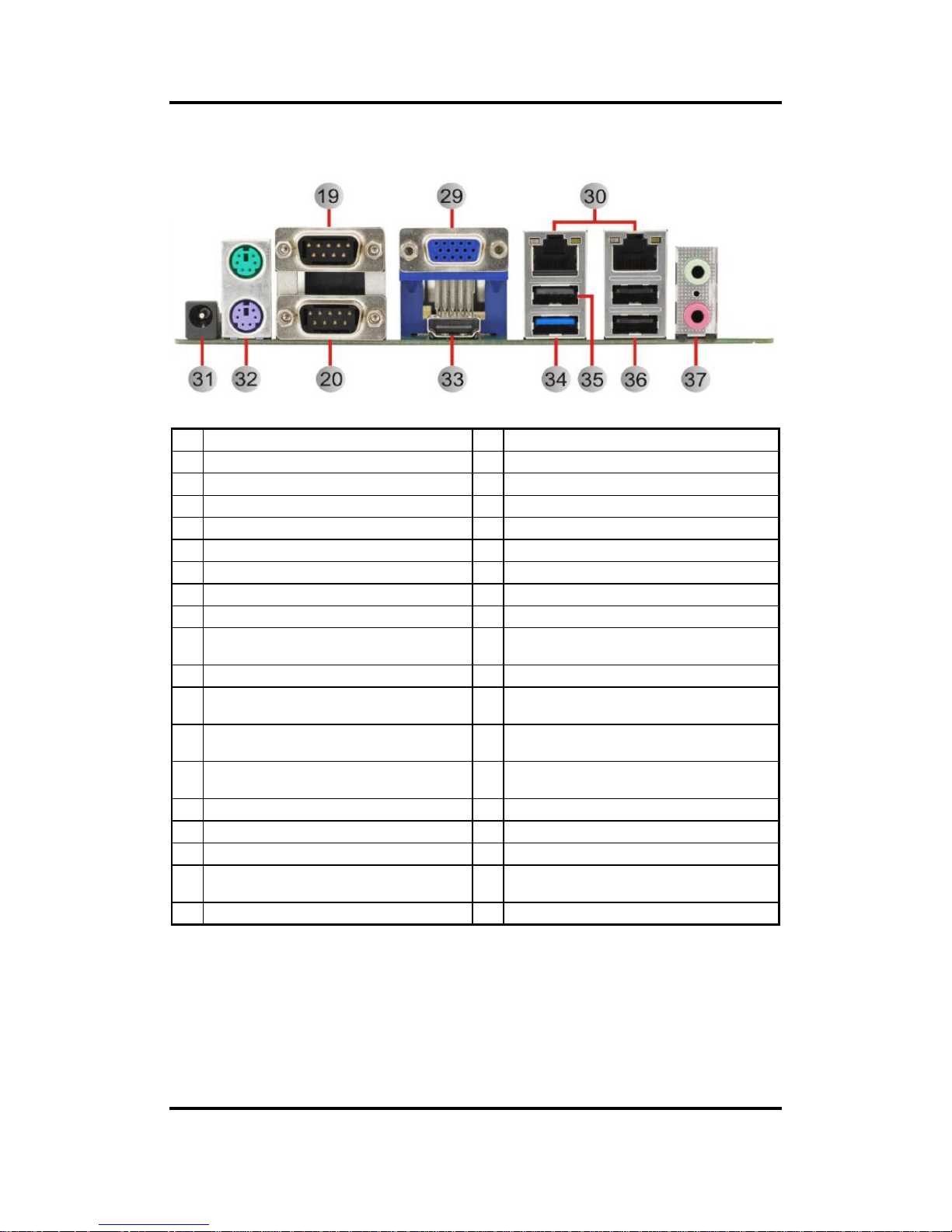
2.2 Rear I/O
1
Front Audio Header (CN31)
20
COM2 Connector (CN18)
2
Internal USB Header (CN3)
21
mSATA Slot (CN28)
3
AT/ATX Power Mode Select Jumper (JP4)
22
PCI-Express x1 Slot (CN26)
4
COM3 Data/Power Select Jumper (JP11)
23
PCI-Express Mini Card Connector (CN27)
5
COM3~COM6 Headers (CN19~CN22)
24
SATA 2.0 Connector (CN4)
6
Power Button Header (CN13)
25
Debug Header (CN2)
7
Fan2 Connector (CN34)
26
DDR3L SO-DIMM Socket (CN23)
8
GPIO Header (CN17)
27
ATX Power Input Connector (CN32)
9
Front Panel Header (CN14)
28
SIM Card Slot (CN5)
10
DC12V/5V Power Output Connector
(CN15)
29
VGA Connector (CN8)
11
Fan1 Connector (CN33)
30
LAN Connectors (CN24~CN25)
12
COM1 RS-232/422/485 Mode Select
Jumpers (JP5~JP7)
31
DC12V Power Input Connector 2 (CN11)
13
DC12V Power Input Connector 1 (CN12)
32
PS/2 Keyboard and Mouse Connector
(CN16)
14
COM2 RS-232/422/485 Mode Select
Jumpers (JP8~JP10)
33
HDMI Connector (CN29)
15
LVDS Backlight Control Header (CN10)
34
USB 3.0 Connector (CN25)
16
LVDS VDD Select Jumper (JP2)
35
USB 2.0 Connector (CN25)
17
LVDS Signal Header (CN9)
36
USB 2.0 Connectors (CN24)
18
LVDS Backlight PWM/CCFL Select Jumper
(JP3)
37
Audio Connector (CN30)
19
COM1 Connector (CN18)
Page 13
MANO842 Mini ITX Motherboard
Board and Pin Assignments 7
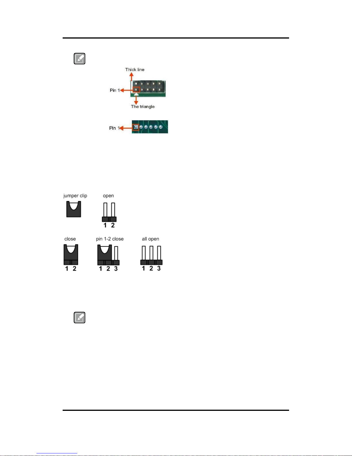
Note
To identify the first pin of a header or jumper, please refer to the following
information:
Usually, there is a thick line or a triangle near the header or jumper pin 1.
Square pad, which you can find on the back of the motherboard, is usually
used for pin 1.
2.3 Jumper Settings
Jumper is a small component consisting of jumper clip and jumper pins. Install jumper clip on 2
jumper pins to close. And remove jumper clip from 2 jumper pins to open. The following
illustration shows how to set up jumper.
Before applying power to MANO842 Series, please make sure all of the jumpers are in factory
default position. Below you can find a summary table of all jumpers and onboard default
settings.
Note
Once the default jumper setting needs to be changed, please do it under power-off
condition.
Page 14

MANO842 Mini ITX Motherboard
8 Board and Pin Assignments
Jumper
Description
Setting
JP1
Clear CMOS
1-2 Close
JP2
LVDS VDD Select
Default: +3.3V
1-2 Close
JP3
LVDS Backlight PWM/CCFL Select
Default: PWM
1-2 Close
JP4
AT/ATX Power Mode Select
Default: ATX Mode
1-2 Close
JP5
COM1 RS-232/422/485 Mode Select
Default: RS-232
1-2 Close
JP6
3-5, 4-6 Close
JP7
3-5, 4-6 Close
JP8
COM2 RS-232/422/485 Mode Select
Default: RS-232
1-2 Close
JP9
3-5, 4-6 Close
JP10
3-5, 4-6 Close
JP11
COM3 Data/Power Select
Default: RS-232 Data
COM3 Pin 1: DCD#
7-9 Close
COM3 Pin 8: RI#
8-10 Close
2.3.1 Clear CMOS Select (JP1)
This jumper allows you to clear the Real Time Clock (RTC) RAM in CMOS. You can
clear the CMOS memory of date, time, and system setup parameters by erasing the
CMOS RTC RAM data. The onboard button cell battery powers the RAM data in CMOS,
which includes system setup information such as system passwords.
To erase the RTC RAM:
1. Turn OFF the computer and unplug the power cord.
2. Remove the onboard battery.
3. Move the jumper clip from pins 1-2 (default) to pins 2-3. Keep the clip on pins 2-3
for about 5~10 seconds, then move the clip back to pins 1-2.
4. Re-install the battery.
5. Plug the power cord and turn ON the computer.
6. Hold down the <Del> key during the boot process and enter BIOS setup to re-enter
data.
2.3.2 LVDS VDD Select (JP2)
This motherboard supports voltage selection for flat panel displays. Use this 3x2-pin
p=2.54mm jumper to set up VDD power of the LVDS connector. To prevent hardware
damage, before connecting please make sure that the input voltage of LVDS panel is
correct.
Function
Setting
Normal operation (Default)
1-2 close
Clear CMOS
2-3 close
Function
Setting
+3.3V (Default)
1-2 close
+5V
3-4 close
+12V
5-6 close
Page 15

MANO842 Mini ITX Motherboard
Board and Pin Assignments 9
2.3.3 LVDS Backlight PWM/CCFL Select (JP3)
This 3x1-pin p=2.54mm jumper enables you to select PWM or voltage control mode for
LVDS backlight control header (CN10). These two control modes are for adjusting the
brightness of LVDS panel.
2.3.4 AT/ATX Power Mode Select (JP4)
This 3x1-pin p=2.54mm jumper allows you to select AT or ATX power mode.
2.3.5 COM1 RS-232/422/485 Mode Select (JP5, JP6, JP7)
Use these jumpers (3x2-pin p=2.54mm) to set COM1 port to operate as RS-232, RS-422
or RS-485 communication mode.
2.3.6 COM2 RS-232/422/485 Mode Select (JP8, JP9, JP10)
Use these jumpers (3x2-pin p=2.54mm) to set COM2 port to operate as RS-232, RS-422
or RS-485 communication mode.
Function
Setting
Controlled by PWM (Default)
1-2 close
Controlled by DC Voltage
2-3 close
Function
Setting
ATX mode (Default)
1-2 close
AT mode
2-3 close
Function
Setting
RS-232 mode
(Default)
JP5 1-2 close
JP6 3-5, 4-6 close
JP7 3-5, 4-6 close
RS-422 mode
JP5 3-4 close
JP6 1-3, 2-4 close
JP7 1-3, 2-4 close
RS-485 mode
JP5 5-6 close
JP6 1-3, 2-4 close
Function
Setting
RS-232 mode
(Default)
JP8 1-2 close
JP9 3-5, 4-6 close
JP10 3-5, 4-6 close
RS-422 mode
JP8 3-4 close
JP9 1-3, 2-4 close
JP10 1-3, 2-4 close
RS-485 mode
JP8 5-6 close
JP9 1-3, 2-4 close
Page 16

MANO842 Mini ITX Motherboard
10 Board and Pin Assignments
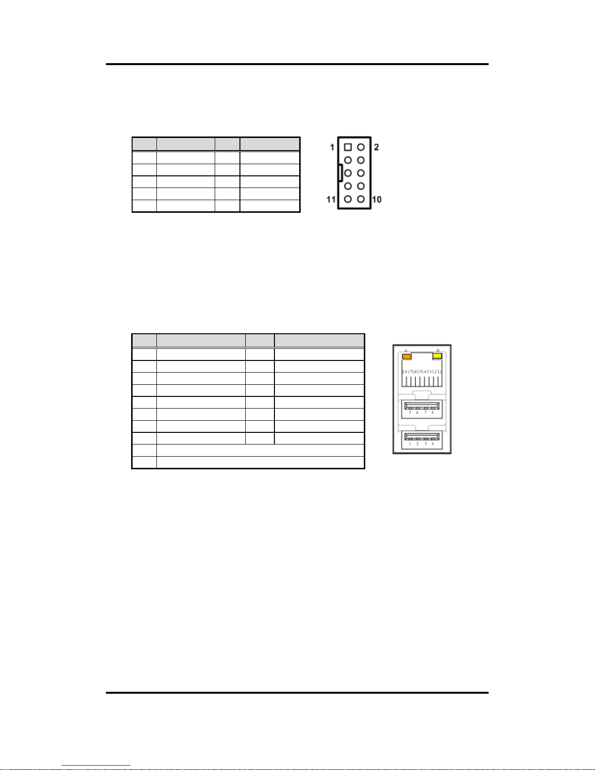
2.3.7 COM3 Data/Power Select (JP11)
The COM3 port has +5V/+12V power capability on DCD and +5V/+12V on RI by setting
this 5x2-pin p=2.54mm jumper.
Function
Setting
Power: Set COM3 pin 1 to +12V level
1-3 close
Power: Set COM3 pin 1 to +5V level
3-5 close
Data: Set COM3 pin 1 to DCD# (Default)
7-9 close
Power: Set COM3 pin 8 to +12V level
2-4 close
Power: Set COM3 pin 8 to +5V level
4-6 close
Data: Set COM3 pin 8 to RI# (Default)
9-10 close
Page 17
MANO842 Mini ITX Motherboard
Board and Pin Assignments 11
2.4 Connectors
Signals go to other parts of the system through connectors. Loose or improper connection
might cause problems, please make sure all connectors are properly and firmly connected.
Here is a summary table showing connectors on the hardware.
Connector
Description
CN3
Internal USB 2.0 Header
CN4
SATA 2.0 Connector
CN5
SIM Card Slot
CN8
VGA Connector
CN9
LVDS Signal Header
CN10
LVDS Backlight Control Header
CN11
DC12V Power Input Connector 2
CN12
DC12V Power Input Connector 1
CN13
Power Button Header
CN14
Front Panel Header
CN15
DC12V/5V Power Output Connector
CN16
PS/2 Keyboard and Mouse Connector
CN17
GPIO Header
CN18
COM1~COM2 Connector
CN19~CN22
COM3~COM6 Headers
CN23
DDR3L SO-DIMM Socket
CN24
LAN and USB 2.0 Connector
CN25
LAN, USB 3.0 and USB 2.0 Connector
CN26
PCI-Express x1 Slot
CN27
PCI-Express Mini Card Connector
CN28
mSATA Slot
CN29
HDMI Connector
CN30
Audio Connector
CN31
Front Audio Header
CN32
ATX Power Input Connector
CN33
Fan1 Connector
CN34
Fan2 Connector
Page 18

MANO842 Mini ITX Motherboard
12 Board and Pin Assignments
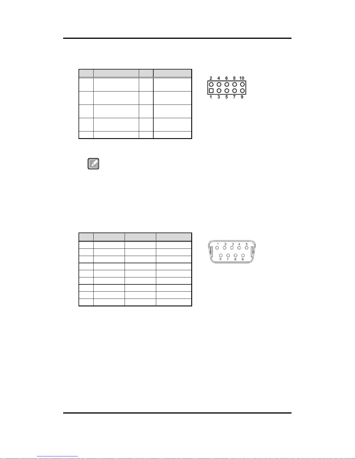
2.4.1 Internal USB Header (CN3)
This is USB 2.0 header (5x2-pin p=2.54mm).
2.4.2 SATA Connectors (CN4)
This connector supports SATA 2.0.
2.4.3 SIM Card Slot (CN5)
The CN5 is for inserting SIM Card. It is mainly used in 3G wireless network application.
In order to work properly, the SIM Card must be used together with 3G module which is
inserted to CN27.
Pin
Signal
Pin
Signal
1
+5V 2 +5V 3 USB1-
4
USB2-
5
USB1+
6
USB2+
7
GND
8
GND
9
N/C
10
N/C
Pin
Signal
1
GND
2
SATA_TXP2
3
SATA_TXN2
4
GND
5
SATA_RXN2
6
SATA_RXP2
7
GND
Pin
Signal
1
PWR
2
RST 3 CLK 4 NC 5 GND
6
VPP 7 I/O 8 NC
SATA
Page 19
MANO842 Mini ITX Motherboard
Board and Pin Assignments 13
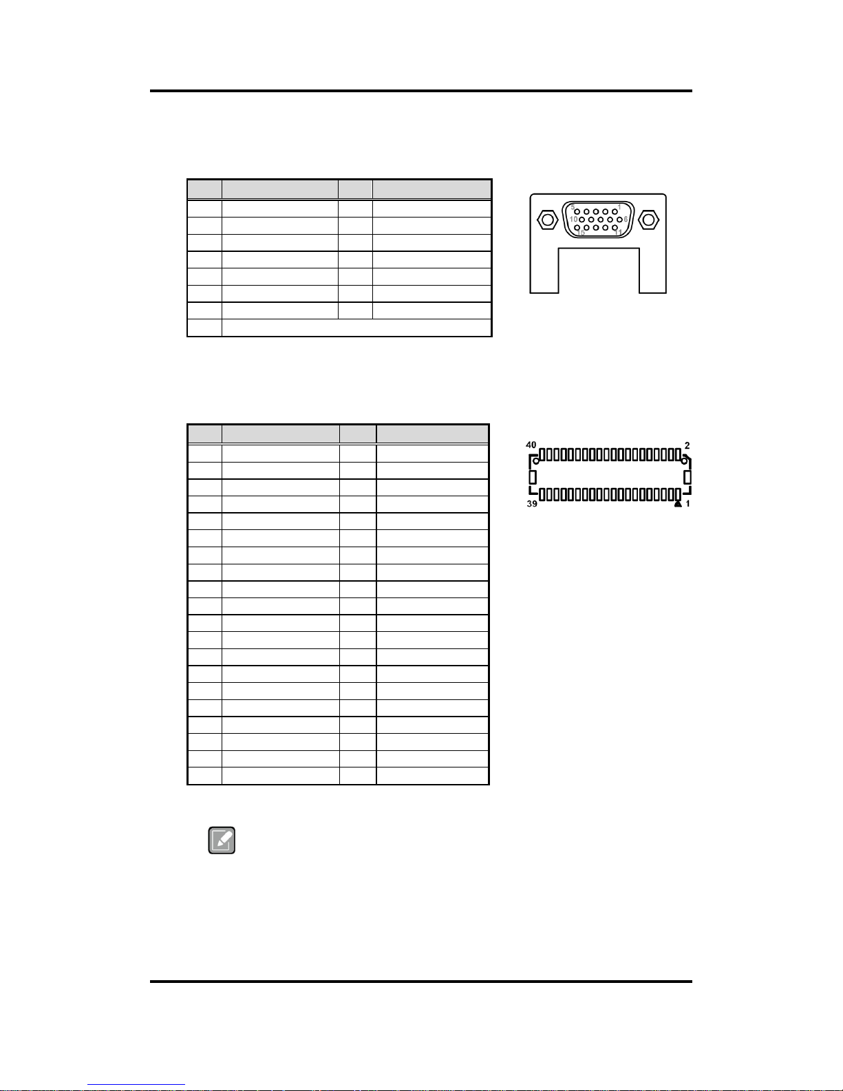
2.4.4 VGA Connector (CN8)
The CN8 is a high rise 15-pin D-Sub connector which is commonly used for VGA monitor.
This VGA interface configuration can be configured via software utility.
2.4.5 LVDS Signal Header (CN9)
This motherboard has a 20x2-pin p=1.00mm header for LVDS panel interface.
Note
[*]
: Panel power VDD is +3.3V by default. This VDD signal is selectable by
jumper JP2, see section 2.3.2.
[**]
: Grounding of this pin is required to ensure normal LVDS output.
[***]
: Connector type: GeanLea GLA1001WV-S-2X20 for reference.
Pin
Signal
Pin
Signal
1
Red 2 Green
3
Blue 4 N.C. 5 GND
6
DETECT
7
GND
8
GND
9
VCC
10
GND
11
N.C.
12
DDC DATA
13
Horizontal Sync
14
Vertical Sync
15
DDC CLK
Pin
Signal
Pin
Signal
1
VDD
[*]
2
VDD
[*]
3
VDD
[*]
4
VDD
[*]
5
VDD
[*]
6
VDD
[*]
7
N/C 8 N/C
9
GND
10
GND
11
LVDS_B_DATA3-
12
LVDS_B_DATA0-
13
LVDS_B_DATA3+
14
LVDS_B_DATA0+
15
GND
16
GND
17
LVDS_B_CLK-
18
LVDS_B_DATA1-
19
LVDS_B_ CLK +
20
LVDS_B_DATA1+
21
GND
22
GND
23
LVDS_A_DATA0-
24
LVDS_B_DATA2-
25
LVDS_A_DATA0+
26
LVDS_B_DATA2+
27
GND
28
GND
29
LVDS_A_DATA1-
30
LVDS_A_DATA3-
31
LVDS_A_DATA1+
32
LVDS_A_DATA3+
33
GND(Detect)
[**]
34
GND
35
LVDS_A_DATA2-
36
LVDS_A_CLK-
37
LVDS_A_DATA2+
38
LVDS_A_ CLK +
39
GND
40
GND
Page 20

MANO842 Mini ITX Motherboard
14 Board and Pin Assignments
2.4.6 LVDS Backlight Control Header (CN10)
This is an 8x1-pin p=1.25mm header for LVDS backlight control interface.
Note
[*]
: This signal is selectable by jumper JP3, see section 2.3.3.
[**]
: Connector type: GeanLea GLA1252WV-S-F-8P for reference.
2.4.7 DC12V Power Input Connector 1 (CN12)
This is a 4-pin connector for DC +12V power input.
2.4.8 Power Button Header (CN13)
This is power button header (2x1-pin p=2.54mm).
Pin
Signal
1
+12V
2
+12V
3
+5V 4 LVDS_BKL_EN
5
GND
6
GND
7
GND
8
LVDS_BKL_CTL
[*]
Pin
Signal
1
GND
2
GND
3
+ 12V IN
4
+ 12V IN
Pin
Signal
1
PWR+
2
PWR-
1
Page 21

MANO842 Mini ITX Motherboard
Board and Pin Assignments 15
2.4.9 Front Panel Header (CN14)
This is front panel header (7x2-pin p=2.54mm).
Note
[*]
: The motherboard’s own buzzer will be active when pin 2 and pin 4 is
connecting, the external speaker on chassis will be active when pin 2 and
pin 4 is open.
2.4.10 DC12V/5V Power Output Connector (CN15)
This is a 4x1-pin p=2.54mm connector for DC +12V and +5V power output.
2.4.11 PS/2 Keyboard and Mouse Connector (CN16)
The board has two 6-pin mini-DIN PS/2 connectors; green for mouse and purple for
keyboard.
Pin
Signal
1
Power LED+
2
SPK-
[*]
3
GND
4
BUZZER
5
Power LED-
6
N/C
7
N/C
8
SPK+
[*]
9
PWR-
10
PWR+
11
RESET-
12
RESET+
13
HD LED-
14
HD LED+
Pin
Signal
1
+12V
2
GND
3
GND
4
+5V
Pin
Signal
Pin
Signal
1
K/B Data
7
M/S Data
2
NC 8 NC 3 GND
9
GND
4
+5V
10
+5V 5 K/B CLK
11
M/S CLK
6
NC
12
NC
Page 22
MANO842 Mini ITX Motherboard
16 Board and Pin Assignments
2.4.12 GPIO Header (CN17)
This header (5x2-pin p=2.54mm) is for digital I/O interface.
Note
[*]
: “H” or “L” means the default voltage is High or Low level, and GPIO
output is 5V.
2.4.13 COM Connector (CN18)
This connector is for COM1 and COM2 serial port interfaces which are selectable for
RS-232/422/485 mode. If you need COM1 to support RS-422 or RS-485, please refer to
section 2.3.5. If you need COM2 to support RS-422 or RS-485, please refer to section
2.3.6. The pin assignments of RS-232/422/485 are listed in table below.
Pin
Signal
Pin
Signal
1
SIO_GPO74
(0xA06, Bit4, H)
[*]
2
SIO_GPI70
(0xA06, Bit0)
3
SIO_GPO75
(0xA06, Bit5, H)
[*]
4
SIO_GPI71
(0xA06, Bit1)
5
SIO_GPO76
(0xA06, Bit6, H)
[*]
6
SIO_GPI72
(0xA06, Bit2)
7
SIO_GPO77
(0xA06, Bit7, H)
[*]
8
SIO_GPI73
(0xA06, Bit3)
9
GND
10
GND
Pin
RS-232
RS-422
RS-485
1
DCD#
TX-
485- 2 RXD
TX+
485+
3
TXD
RX+
N/C 4 DTR#
RX-
N/C 5 GND
GND
GND
6
DSR#
N/C
N/C 7 RTS#
N/C
N/C 8 CTS#
N/C
N/C 9 RI#
N/C
N/C
Page 23
MANO842 Mini ITX Motherboard
Board and Pin Assignments 17
CN24
2.4.14 COM Headers (CN19~CN22)
The motherboard comes with 5x2-pin p=2.54mm headers for COM3~COM6 serial port
interfaces. Only COM3 comes with power capability on DCD# and RI# pins by setting
JP11 (see section 2.3.7).
2.4.15 LAN and USB Connectors (CN24 and CN25)
The board comes with two high performance plug and play Ethernet interfaces (RJ-45)
which are fully compliant with the IEEE 802.3 standard. Connection can be established
by plugging one end of the Ethernet cable into this RJ-45 connector and the other end to
a 1000/100/10-Base-T hub.
The CN24 has lower double-deck connector for USB 2.0 port 1 and 2.
Pin
Signal
Pin
Signal
1
DCD#
2
DSR#
3
RXD
4
RTS#
5
TXD 6 CTS#
7
DTR#
8
RI# 9 GND
10
N/C
Pin
LAN2 Signal
Pin
USB Signal
L1
MDI0+
1
+5V standby power
L2
MDI0-
2
USB D1-
L3
MDI1+
3
USB D1+
L4
MDI1-
4
Ground (GND)
L5
MDI2+
5
+5V standby power
L6
MDI2-
6
USB D2-
L7
MDI3+
7
USB D2+
L8
MDI3-
8
Ground (GND)
A
100 LAN LED (Green)/1000 LAN LED (Orange)
B
Active LED (Yellow)
Page 24
MANO842 Mini ITX Motherboard
18 Board and Pin Assignments
The CN25 has lower double-deck connector for USB 3.0 port 1 and USB 2.0 port 3.
CN25
2.4.16 PCI-Express x1 Slot (CN26)
This board has one PCI-Express x1 slot.
Pin
LAN1 Signal
Pin
LAN1 Signal
L1
MDI0+
L5
MDI2+
L2
MDI0-
L6
MDI2-
L3
MDI1+
L7
MDI3+
L4
MDI1-
L8
MDI3-
A
100 LAN LED (Green)/1000 LAN LED (Orange)
B
Active LED (Yellow)
Pin
USB 3.0 Signal
Pin
USB 2.0 Signal
1
USB_VCC (+5V
standby power)
1
+5V standby power
2
USB_Data0-
2
USB D1-
3
USB_Data0+
3
USB D1+
4
GND
4
Ground (GND)
5
SSRX1-
6
SSRX1+
7
GND
8
SSTX1-
9
SSTX1+
Pin
Signal
Pin
Signal
B1
+12V
A1
PRSNT1#
B2
+12V
A2
+12V
B3
RSVD
A3
+12V
B4
GND
A4
GND
B5
SMCLK
A5
NC
B6
SMDAT
A6
NC
B7
GND
A7
NC
B8
+3.3V
A8
NC
B9
NC
A9
+3.3V
B10
3.3Vaux
A10
+3.3V
B11
WAKE#
A11
PERST#
B12
NC
A12
GND
B13
GND
A13
REFCLK+
B14
HSOP0
A14
REFCLK-
B15
HSON0
A15
GND
B16
GND
A16
HSIP0
B17
NC
A17
HSIN0
B18
GND
A18
GND
Page 25
MANO842 Mini ITX Motherboard
Board and Pin Assignments 19
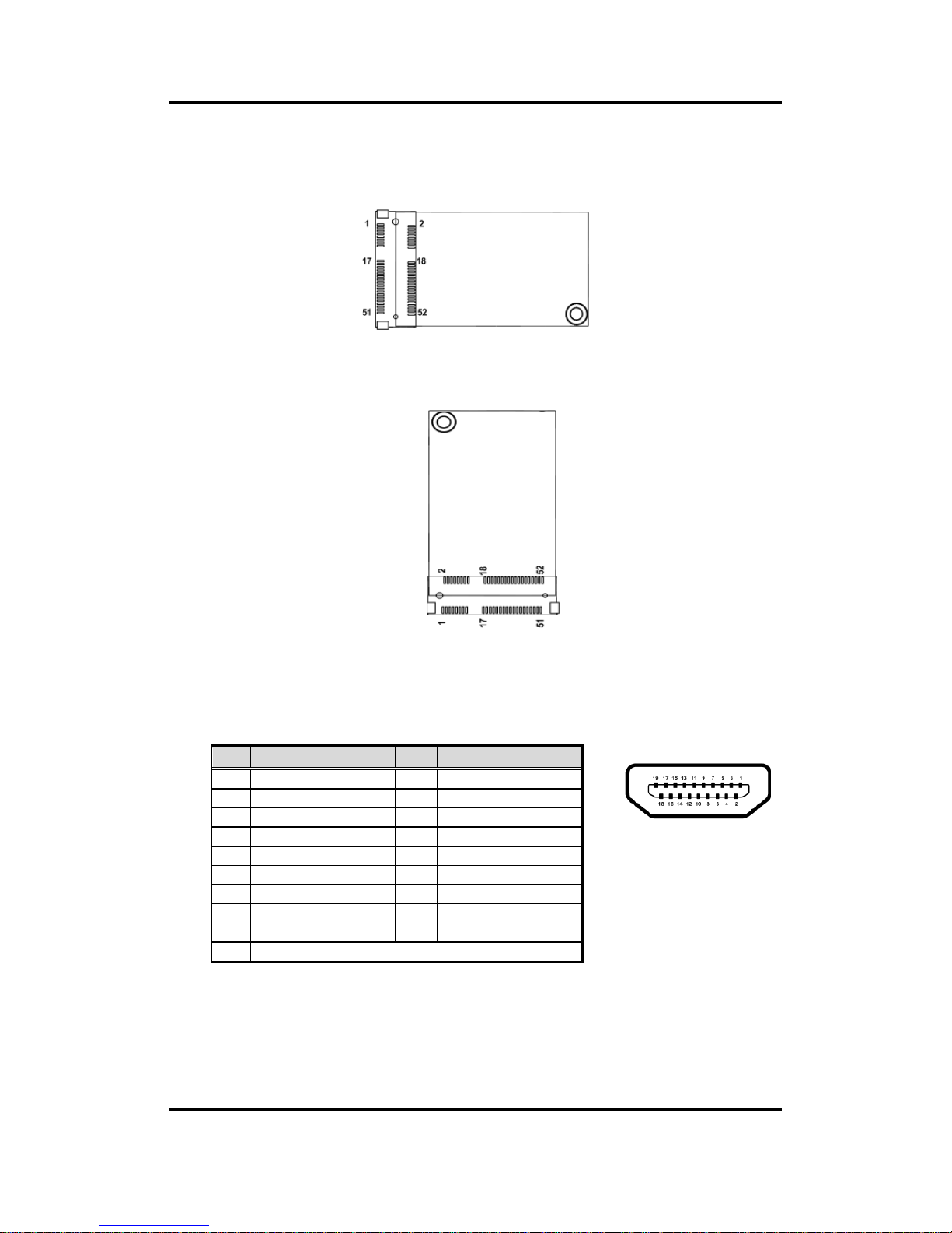
2.4.17 Full-size PCI-Express Mini Card Connector (CN27)
This is a PCI-Express Mini Card connector applying to PCI-Express or USB 2.0. It
complies with PCI-Express Mini Card Spec. V1.2.
2.4.18 mSATA Slot (CN28)
2.4.19 HDMI Connector (CN29)
The HDMI (High-Definition Multimedia Interface) interface is available through this
connector.
19 1
18 2
Pin
Signal
Pin
Signal
1
HDMI OUT_DATA2+
2
GND
3
HDMI OUT_DATA2-
4
HDMI OUT_DATA1+
5
GND
6
HDMI OUT_DATA1-
7
HDMI OUT_DATA0+
8
GND
9
HDMI OUT_DATA0-
10
HDMI OUT_Clock+
11
GND
12
HDMI OUT_Clock-
13
N.C.
14
N.C.
15
HDMI OUT_SCL
16
HDMI OUT_SDA
17
GND
18
+5V
19
HDMI_HTPLG
Page 26

MANO842 Mini ITX Motherboard
20 Board and Pin Assignments
2.4.20 Audio Jack (CN30)
The board provides HD audio jack on the rear I/O. Install audio driver, and then attach
audio devices to CN30.
2.4.21 Front Audio Header (CN31)
This is front audio header (5x2-pin p=2.00mm) for convenient connection and control of
audio devices.
2.4.22 Fan Connectors (CN33 and CN34)
This motherboard has two fan connectors. You can find fan speed option(s) at BIOS
Setup Utility. For further information, see BIOS Setup Utility: Advanced\HW Monitor\PC
Health Status.
The CN33 (4x1-pin p=2.54mm) is for Fan1 interface.
The CN34 (3x1-pin p=2.54mm) is for Fan2 interface.
Pin Color
Signal
Green
Line-out
Pink
MIC-in
Pin
Signal
Pin
Signal
1
FP_MIC_IN
2
GND
3
FP_IN_L
4
GND
5
FP_IN_R
6
GND
7
FP_OUT_L
8
GND
9
FP_OUT_R
10
GND
Pin
Signal
1
GND
2
+12V
3
FAN Speed Detection
4
FAN Speed Control
Pin
Signal
1
GND
2
+12V
3
FAN Speed Detection
Page 27

MANO842 Mini ITX Motherboard
Hardware Description 21
Chapter 3
Hardware Description
3.1 Microprocessors
The MANO842 Series supports Intel® Celeron® J1900 processor, which enable your system to
operate under Windows® 7, Windows® 8, Windows® 8.1 and Linux environments. The system
performance depends on the microprocessor. Make sure all correct settings are arranged for
your installed microprocessor to prevent the CPU from damages.
3.2 BIOS
The MANO842 Series uses AMI Plug and Play BIOS with a single SPI Flash.
3.3 System Memory
The MANO842 supports one 204-pin DDR3L SO-DIMM socket for maximum memory capacity
up to 8GB DDR3L SDRAMs. The memory module comes in sizes of 1GB, 2GB, 4GB and 8GB.
Page 28

MANO842 Mini ITX Motherboard
22 Hardware Description
This page is intentionally left blank.
Page 29

MANO842 Mini ITX Motherboard
AMI BIOS Setup Utility 23
Chapter 4
AMI BIOS Setup Utility
The AMI UEFI BIOS provides users with a built-in setup program to modify basic system
configuration. All configured parameters are stored in a flash chip to save the setup information
whenever the power is turned off. This chapter provides users with detailed description about
how to set up basic system configuration through the AMI BIOS setup utility.
4.1 Starting
To enter the setup screens, follow the steps below:
1. Turn on the computer and press <Del> during the Power On Self Test (POST) to enter
BIOS setup, otherwise, POST will continue with its test routines.
2. Once you enter the BIOS, the main BIOS setup menu displays. You can access the other
setup screens from the main BIOS setup menu, such as the Advanced and Chipset
menus.
Note
If your computer cannot boot after making and saving system changes with BIOS
setup, you can restore BIOS optimal defaults by setting JP1 (see section 2.3.1).
It is strongly recommended that you should avoid changing the chipset’s defaults. Both AMI
and your system manufacturer have carefully set up these defaults that provide the best
performance and reliability.
4.2 Navigation Keys
The BIOS setup/utility uses a key-based navigation system called hot keys. Most of the BIOS
setup utility hot keys can be used at any time during the setup navigation process. These keys
include <F1>, <F2>, <Enter>, <ESC>, <Arrow> keys, and so on.
Note
Some of the navigation keys differ from one screen to another.
Page 30

MANO842 Mini ITX Motherboard
24 AMI BIOS Setup Utility
Hot Keys
Description
Left/Right
The Left and Right <Arrow> keys allow you to select a setup screen.
Up/Down
The Up and Down <Arrow> keys allow you to select a setup screen or sub
screen.
Enter
The <Enter> key allows you to display or change the setup option listed for a
particular setup item. The <Enter> key can also allow you to display the setup
sub screens.
+ Plus/Minus
The Plus and Minus <Arrow> keys allow you to change the field value of a
particular setup item.
F1
The <F1> key allows you to display the General Help screen.
F2
The <F2> key allows you to Load Previous Values.
F3
The <F3> key allows you to Load Optimized Defaults.
F4
The <F4> key allows you to save any changes you have made and exit Setup.
Press the <F4> key to save your changes.
Esc
The <Esc> key allows you to discard any changes you have made and exit the
Setup. Press the <Esc> key to exit the setup without saving your changes.
Page 31

MANO842 Mini ITX Motherboard
AMI BIOS Setup Utility 25
4.3 Main Menu
When you first enter the setup utility, you will enter the Main setup screen. You can always
return to the Main setup screen by selecting the Main tab. System Time/Date can be set up as
described below. The Main BIOS setup screen is shown below.
BIOS Information
Display the BIOS information.
System Date/Time
Use this option to change the system time and date. Highlight System Time or System Date
using the <Arrow> keys. Enter new values through the keyboard. Press the <Tab> key or the
<Arrow> keys to move between fields. The date must be entered in MM/DD/YY format. The
time is entered in HH:MM:SS format.
Access Level
Display the access level of current user.
Page 32
MANO842 Mini ITX Motherboard
26 AMI BIOS Setup Utility
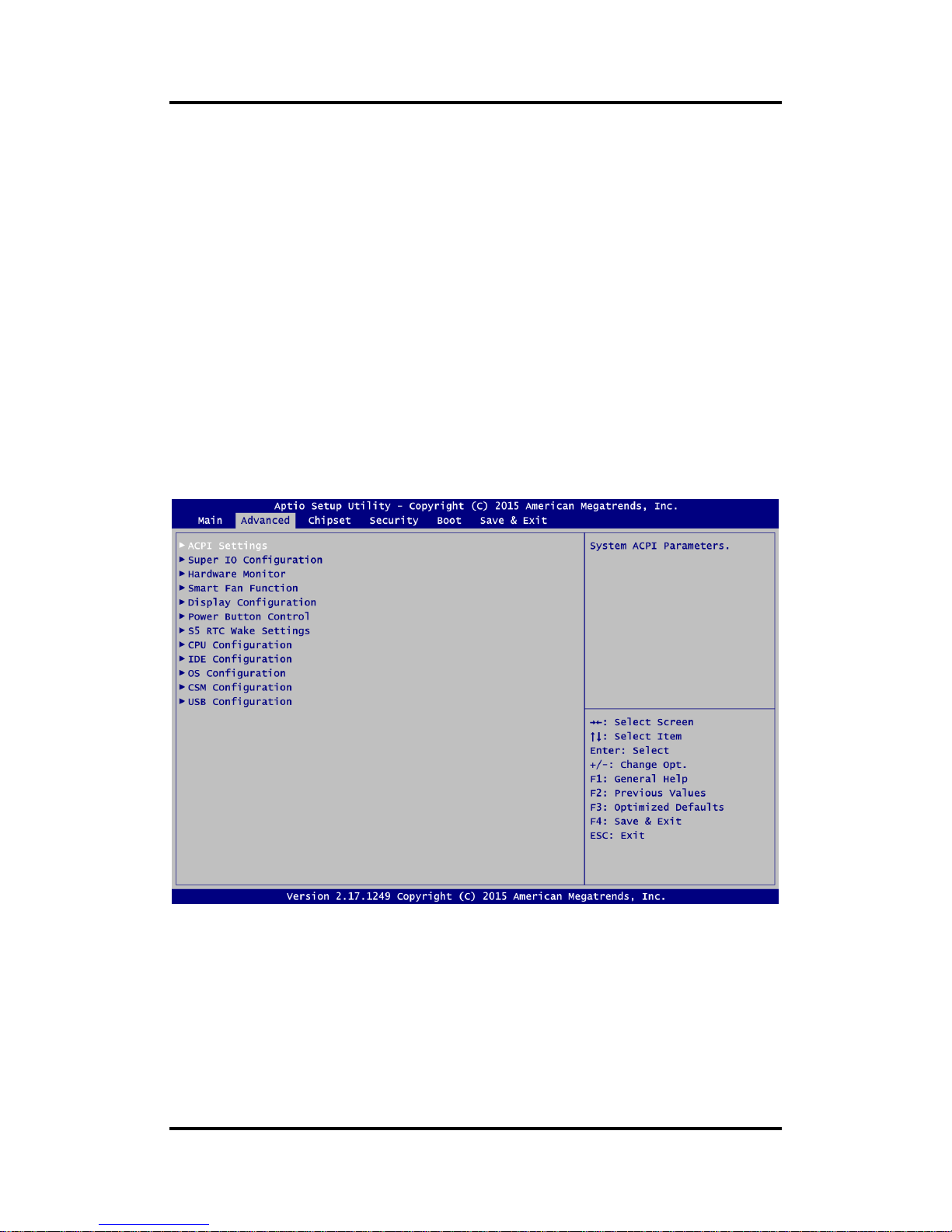
4.4 Advanced Menu
The Advanced menu also allows users to set configuration of the CPU and other system
devices. You can select any of the items in the left frame of the screen to go to the sub menus:
► ACPI Settings
► Super IO Configuration
► Hardware Monitor
► Smart Fan Function
► Display Configuration
► Power Button Control
► S5 RTC Wake Settings
► CPU Configuration
► IDE Configuration
► OS Configuration
► CSM Configuration
► USB Configuration
For items marked with “”, please press <Enter> for more options.
Page 33

MANO842 Mini ITX Motherboard
AMI BIOS Setup Utility 27
ACPI Settings
You can use this screen to select options for the ACPI configuration, and change the value
of the selected option. A description of the selected item appears on the right side of the
screen.
Enable ACPI Auto Configuration
Enable or disable BIOS ACPI auto configuration.
Enable Hibernation
Enable or disable system ability to hibernate (OS/S4 sleep state).
ACPI Sleep State
Select the ACPI (Advanced Configuration and Power Interface) sleep state. Configuration
options are Suspend Disabled and S3 (Suspend to RAM). The default setting is S3
(Suspend to RAM); this option selects ACPI sleep state the system will enter when
suspend button is pressed.
Page 34

MANO842 Mini ITX Motherboard
28 AMI BIOS Setup Utility
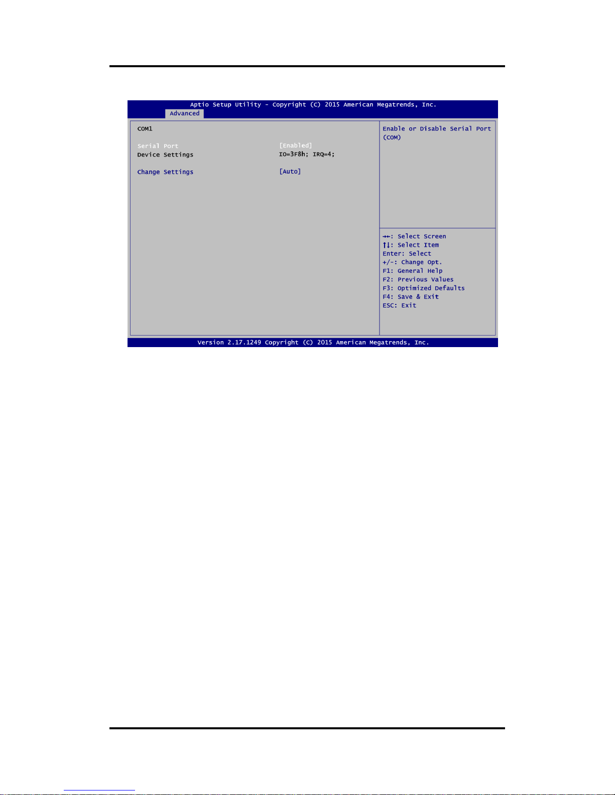
Super IO Configuration
You can use this screen to select options for the Super IO Configuration, and change the
value of the selected option. A description of the selected item appears on the right side of
the screen. For items marked with “”, please press <Enter> for more options.
COM1~6
Use these items to set parameters related to serial port 1~6.
Page 35
MANO842 Mini ITX Motherboard
AMI BIOS Setup Utility 29
COM1
Serial Port
Enable or disable serial port 1. The optimal setting for base I/O address is 3F8h and for
interrupt request address is IRQ4.
Change Settings
Select an optimal setting for serial port.
Page 36
MANO842 Mini ITX Motherboard
30 AMI BIOS Setup Utility
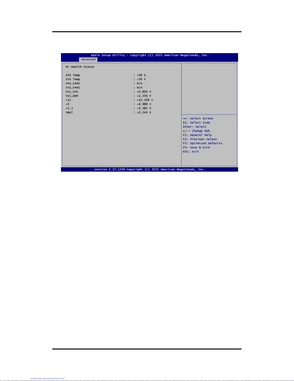
Hardware Monitor
This screen monitors hardware health status.
This screen displays the temperature of system and CPU, cooling fans speed in RPM and
system voltages (VCC_CPU, VCC_DDR, +12V, +5V, +3.3V and VBAT).
Page 37
MANO842 Mini ITX Motherboard
AMI BIOS Setup Utility 31
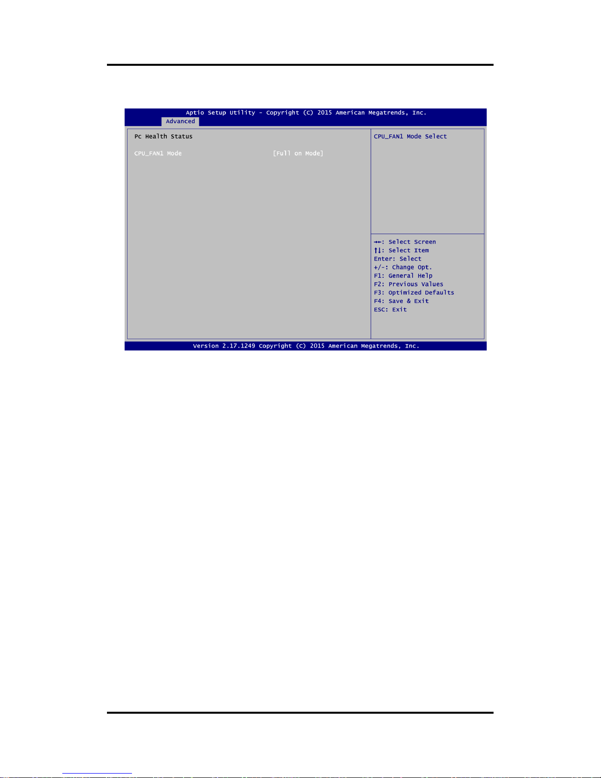
Smart Fan Function
This screen allows you to select the fan mode.
CPU_FAN1 Mode
This item allows you to select the fan mode, which can be set to Full on Mode, Manual
Mode, Auto PWM Mode or Auto RPM Mode.
Page 38
MANO842 Mini ITX Motherboard
32 AMI BIOS Setup Utility
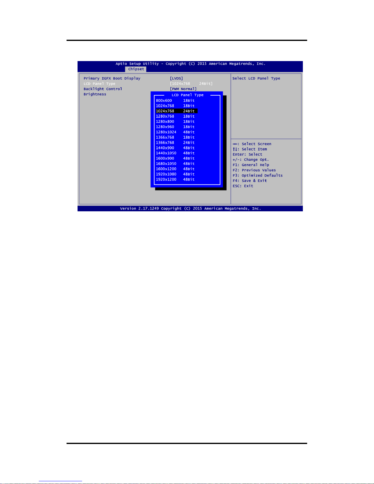
Display Configuration
Primary IGFX Boot Display
Select the video device which will be activated during POST (Power-On Self Test). The
default is LVDS.
Backlight Control
Select panel backlight control mode.
LVDS Panel Type
Select LVDS panel resolution; see the selection options in image above.
Brightness
Select the brightness of LVDS panel ranging from 30% to 100%. The default setting is
70%.
Page 39

MANO842 Mini ITX Motherboard
AMI BIOS Setup Utility 33
Power Button Control
Restore AC Power Loss
This item decides the state of system when AC power is resupplied after a power failure.
Mode options are Power Off, Power On and Last State.
Soft-Off by PWR-BTTN
- Instant-Off: The system will shut down instantly when the power button is pressed.
- Delay 4 sec: The system will shut down only when the power button is pressed and held
at least 4 seconds.
PS/2 KB/MS Wake Up From S5
This item decides whether or not the PS/2 keyboard or mouse can wake up the system
from S5 state.
Page 40

MANO842 Mini ITX Motherboard
34 AMI BIOS Setup Utility
S5 RTC Wake Settings
Wake system from S5
Enable or disable system wake on alarm event. It allows you to wake up the system in a
certain time. Select Fixed Time to set the system to wake on the specified time. Use <>
<> to switch among the items: Day, Hour, Minute and Second, and type the value in the
selected item as you wish. For example, if you want the system to start up automatically at
14:25:26, the 13th day of each month, then you should enter 13, 14, 25, and 26 from top to
bottom.
Page 41

MANO842 Mini ITX Motherboard
AMI BIOS Setup Utility 35
CPU Configuration
This screen shows the CPU Configuration, and you can change the value of the selected
option.
Socket 0 CPU Information
This item is for CPU information.
Limit CPUID Maximum
This item allows user to limit the maximum value of CPUID. In Windows XP environment,
this item should be disabled.
Execute Disable Bit
Enable or disable the No-Execution Page Protection Technology.
Intel Virtualization Technology
Enable or disable Intel Virtualization Technology. When enabled, a VMM (Virtual Machine
Mode) can utilize the additional hardware capabilities. It allows a platform to run multiple
operating systems and applications independently, hence enabling a computer system to
work as several virtual systems.
Page 42
MANO842 Mini ITX Motherboard
36 AMI BIOS Setup Utility
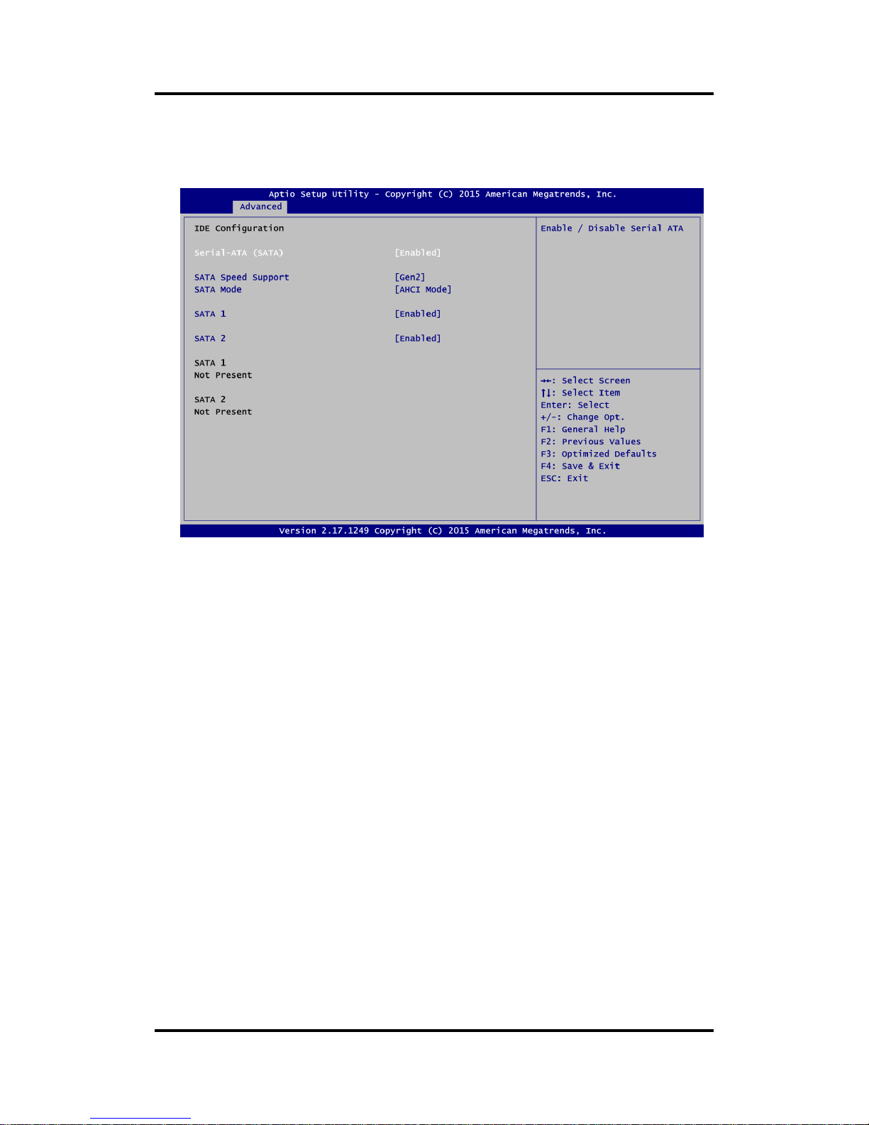
IDE Configuration
In the IDE Configuration menu, you can see the currently installed hardware in the SATA
ports. During system boot up, the BIOS automatically detects the presence of SATA
devices.
Serial-ATA (SATA)
Enable or disable the SATA controller feature.
SATA Speed Support
Select SATA speed support.
SATA Mode
Determine how SATA controller(s) operate. Operation mode options are IDE Mode, AHCI
(Advanced Host Controller Interface) Mode. The default is AHCI Mode.
SATA 1~2
Enable or disable the onboard SATA port 1~2.
Page 43

MANO842 Mini ITX Motherboard
AMI BIOS Setup Utility 37
OS Configuration
OS Selection
This item allows user to select the proper Operating System.
Page 44
MANO842 Mini ITX Motherboard
38 AMI BIOS Setup Utility
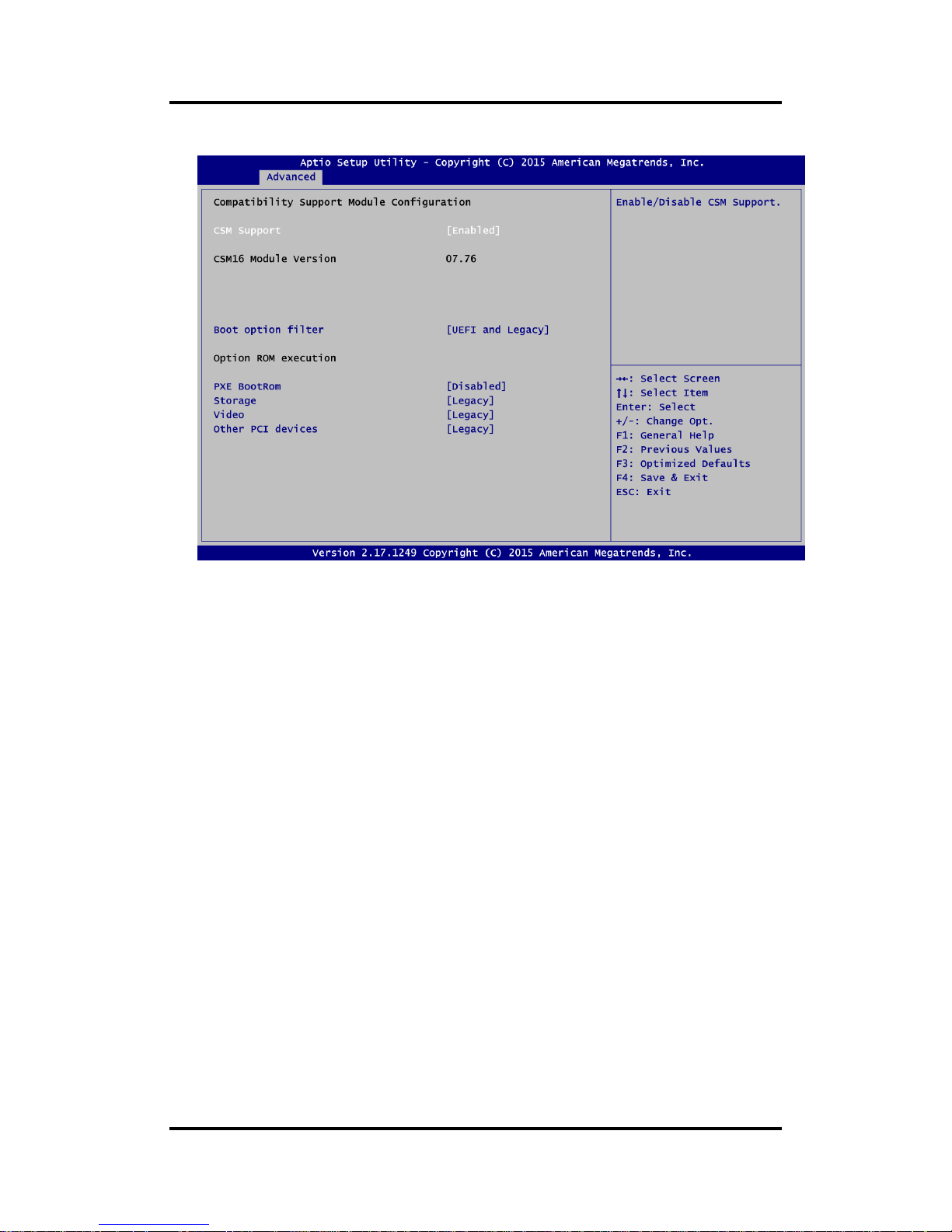
CSM Configuration
CSM Support
Enable or disable CSM (Compatibility Support Module) support.
Boot option filter
Select UEFI or Legacy ROM priority. Default is UEFI and Legacy mode.
PXE BootRom
Enable or disable the Preboot eXecution Environment (PXE) boot ROM function of the
onboard LAN chip during system boots up.
Storage
Select the execution of UEFI or Legacy storage option ROM. Default is Legacy mode.
Video
Select the execution of UEFI or Legacy video option ROM. Default is Legacy mode.
Other PCI devices
Select the execution of UEFI or Legacy option ROM of other PCI-Express network,
storage or video devices. Default is Legacy mode.
Page 45

MANO842 Mini ITX Motherboard
AMI BIOS Setup Utility 39
USB Configuration
USB Devices
Display all detected USB devices.
Legacy USB Support
Use this item to enable or disable legacy support for USB devices. The default setting is
Enabled. Auto option disables legacy support if no USB devices are connected. Disable
option will keep USB devices available only for EFI applications.
XHCI Hand-off
Enable or disable feature for OSes without an XHCI hand-off support.
EHCI Hand-off
Enable or disable feature for OSes without an EHCI hand-off support.
USB Mass Storage Driver Support
Enable or disable USB mass storage driver support.
USB transfer time-out
The time-out value for control, bulk and interrupt transfers.
Device reset time-out
USB mass storage device start unit command time-out.
Device power-up delay
Maximum time the device will take before it properly reports itself to the host controller.
Auto option uses default value: for a root port it is 100ms, for a hub port the delay is taken
from hub descriptor.
Page 46
MANO842 Mini ITX Motherboard
40 AMI BIOS Setup Utility
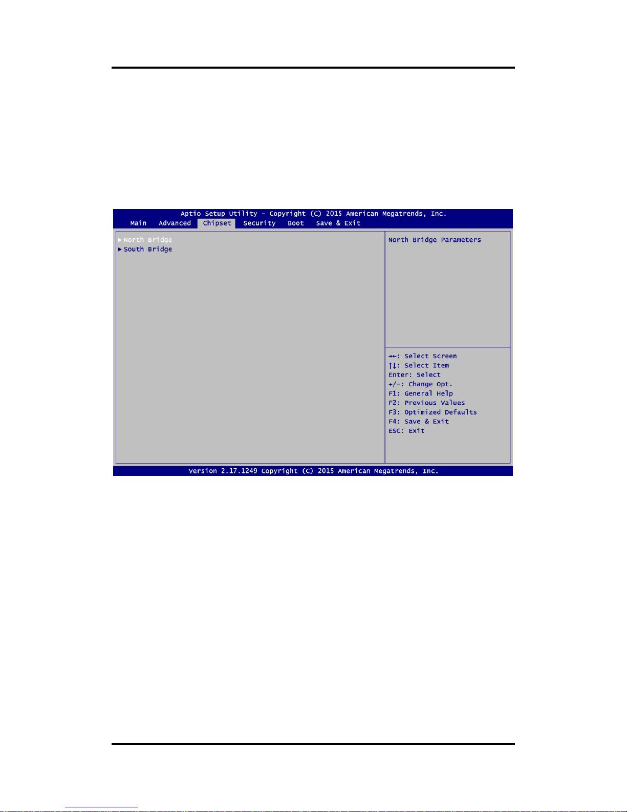
4.5 Chipset Menu
The Chipset menu allows users to change the advanced chipset settings. You can select any
of the items in the left frame of the screen to go to the sub menus:
► North Bridge
► South Bridge
For items marked with “”, please press <Enter> for more options.
Page 47
MANO842 Mini ITX Motherboard
AMI BIOS Setup Utility 41
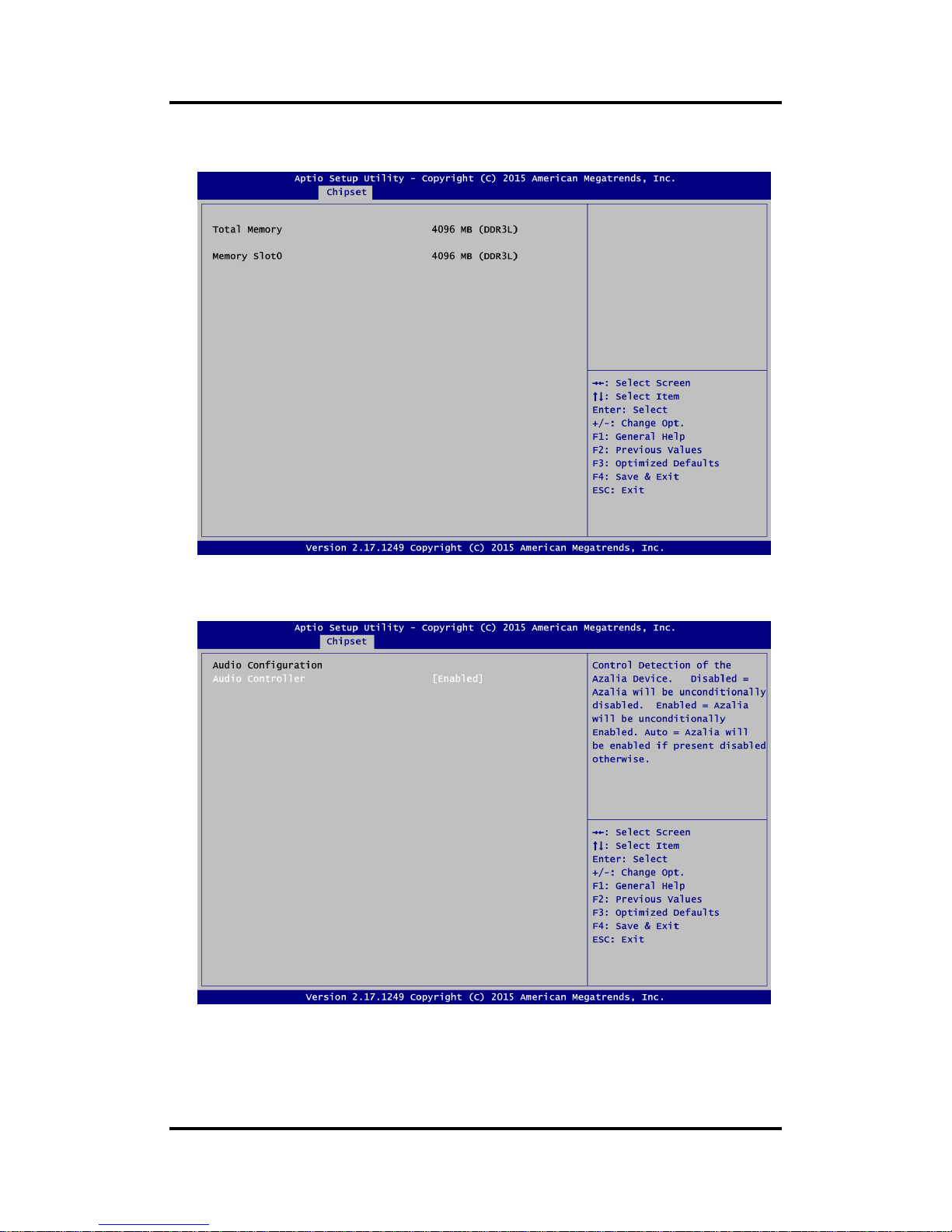
North Bridge
This screen shows system memory information.
South Bridge
This screen allows users to configure parameters of South Bridge chipset.
Audio Controller
Control detection of the audio device.
- Disabled: Audio device will be unconditionally disabled.
- Enabled: Audio device will be unconditionally enabled.
- Auto: If device is present, audio controller will be enabled, otherwise will be disabled.
Page 48
MANO842 Mini ITX Motherboard
42 AMI BIOS Setup Utility
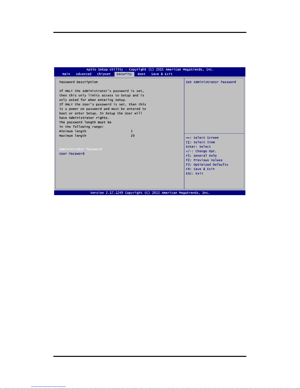
4.6 Security Menu
The Security menu allows users to change the security settings for the system.
Administrator Password
This item indicates whether an administrator password has been set (installed or
uninstalled).
User Password
This item indicates whether a user password has been set (installed or uninstalled).
Page 49
MANO842 Mini ITX Motherboard
AMI BIOS Setup Utility 43
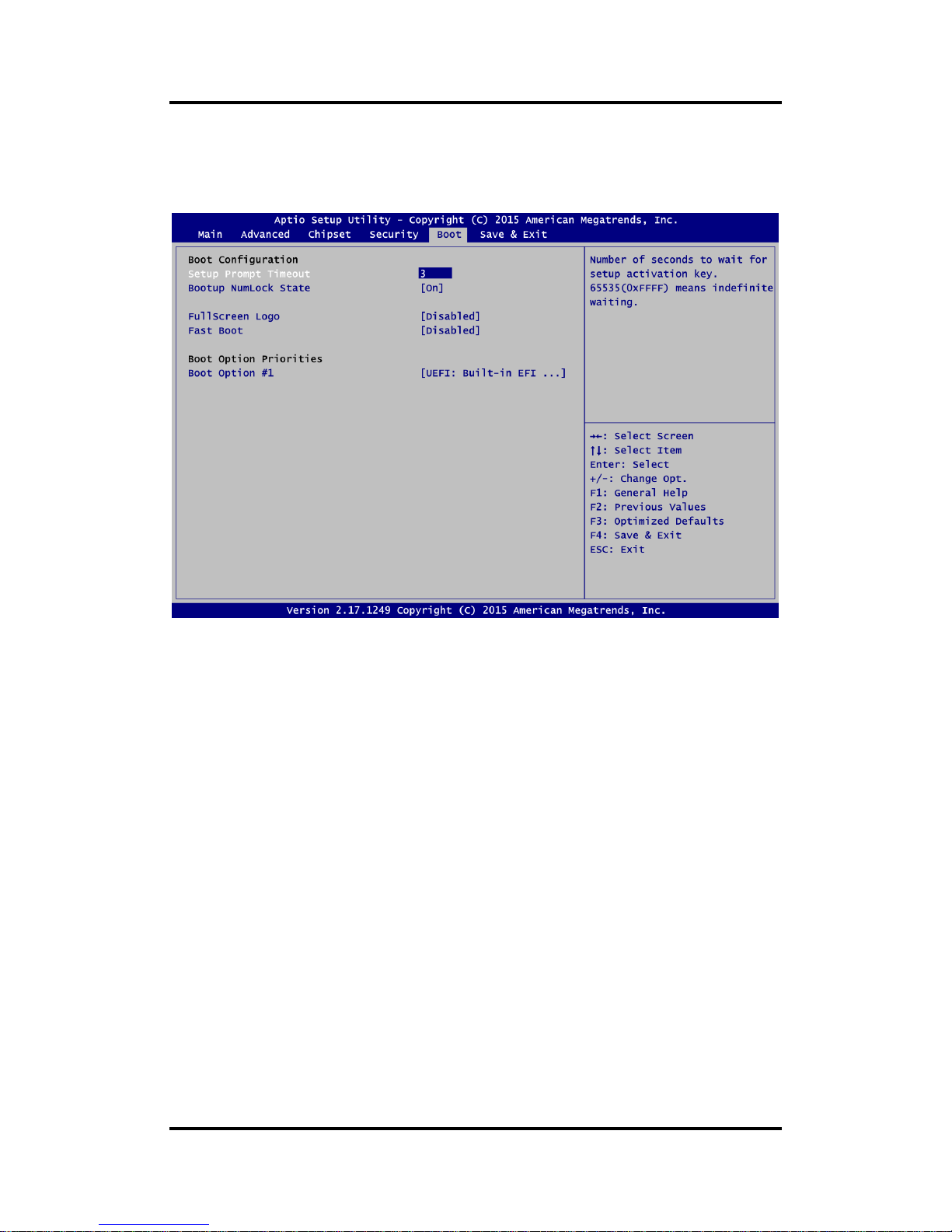
4.7 Boot Menu
The Boot menu allows users to change boot options of the system.
Setup Prompt Timeout
Number of seconds to wait for setup activation key. 65535(0xFFFF) means indefinite
waiting.
Bootup NumLock State
Use this item to select the power-on state for the keyboard NumLock.
FullScreen Logo
Enable or disable OEM logo display at system startup.
Fast Boot
Enable or disable fast boot function. BIOS skips some certain procedures to decrease
system boot up time.
Boot Option Priorities [Boot Option #1, …]
These are settings for boot priority. Specify the boot device priority sequence from the
available devices.
Page 50
MANO842 Mini ITX Motherboard
44 AMI BIOS Setup Utility
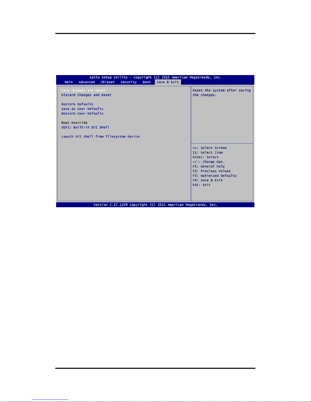
4.8 Save & Exit Menu
The Save & Exit menu allows users to load your system configuration with optimal or fail-safe
default values.
Save Changes and Reset
When you have completed the system configuration changes, select this option to leave
Setup and reboot the computer so the new system configuration parameters can take
effect. Select Save Changes and Reset from the Save & Exit menu and press <Enter>.
Select Yes to save changes and reset.
Discard Changes and Reset
Select this option to quit Setup without making any permanent changes to the system
configuration and reboot the computer. Select Discard Changes and Reset from the Save
& Exit menu and press <Enter>. Select Yes to discard changes and reset.
Restore Defaults
It automatically sets all Setup options to a complete set of default settings when you select
this option. Select Restore Defaults from the Save & Exit menu and press <Enter>.
Save as User Defaults
Select this option to save system configuration changes done so far as User Defaults.
Select Save as User Defaults from the Save & Exit menu and press <Enter>.
Restore User Defaults
It automatically sets all Setup options to a complete set of User Defaults when you select
this option. Select Restore User Defaults from the Save & Exit menu and press <Enter>.
Page 51

MANO842 Mini ITX Motherboard
AMI BIOS Setup Utility 45
Boot Override
Select a drive to immediately boot that device regardless of the current boot order.
Launch EFI Shell from filesystem device
Attempt to launch EFI Shell application (Shellx64.efi) from one of the available filesystem
devices.
 Loading...