

Page 1

MANO520 Series
Intel® Socket 1151 Core
TM
i7/ i5/ i3
Processors Mini ITX Motherboard
User’s Manual
Page 2

ii
Disclaimers
This manual has been carefully checked and believed to contain accurate information.
Axiomtek Co., Ltd. assumes no responsibility for any infringements of patents or any third
party’s rights, and any liability arising from such use.
Axiomtek does not warrant or assume any legal liability or responsibility for the accuracy,
completeness or usefulness of any information in this document. Axiomtek does not make any
commitment to update the information in this manual.
Axiomtek reserves the right to change or revise this document and/or product at any time
without notice.
No part of this document may be reproduced, stored in a retrieval system, or transmitted, in
any form or by any means, electronic, mechanical, photocopying, recording, or otherwise,
without the prior written permission of Axiomtek Co., Ltd.
CAUTION
If you replace wrong batteries, it causes the danger of explosion. It is recommended by the
manufacturer that you follow the manufacturer’s instructions to only replace the same or
equivalent type of battery, and dispose of used ones.
Copyright 2019 Axiomtek Co., Ltd.
All Rights Reserved
January 2019, Version A1
Printed in Taiwan
Page 3

iii
ESD Precautions
Computer boards have integrated circuits sensitive to static electricity. To prevent chipsets
from electrostatic discharge damage, please take care of the following jobs with precautions:
Do not remove boards or integrated circuits from their anti-static packaging until you are
ready to install them.
Before holding the board or integrated circuit, touch an unpainted portion of the system
unit chassis for a few seconds. It discharges static electricity from your body.
Wear a wrist-grounding strap, available from most electronic component stores, when
handling boards and components.
Trademarks Acknowledgments
Axiomtek is a trademark of Axiomtek Co., Ltd.
Intel® and Celeron® are trademarks of Intel Corporation.
Windows® is a trademark of Microsoft Corporation.
AMI is a trademark of American Megatrend Inc.
IBM, PC/AT, PS/2, VGA are trademarks of International Business Machines Corporation.
Other brand names and trademarks are the properties and registered brands of their
respective owners.
Page 4

iv
Table of Contents
Disclaimers ...................................................................................................... ii
ESD Precautions ............................................................................................. iii
Chapter 1 Introduction ............................................. 1
1.1 Features ................................................................................................ 1
1.2 Specifications ........................................................................................ 2
1.3 Utilities Supported ................................................................................. 3
1.4 Block Diagram ....................................................................................... 4
Chapter 2 Board and Pin Assignments .................... 5
2.1 Board Layout ......................................................................................... 5
2.2 Rear I/O ................................................................................................. 6
2.3 Jumper Settings .................................................................................... 7
2.3.1 Clear CMOS (JP1) ...................................................................................... 8
2.3.2 AT/ATX Power Mode Select (JP3) .............................................................. 8
2.3.3 COM1 RS-232/422/485 Mode Select (JP4, JP6, JP7) ............................... 9
2.3.4 COM1 Data/Power Select (JP5) ................................................................. 9
2.3.5 LVDS Backlight PWM/DC Mode Select (JP8) ............................................. 9
2.3.6 LVDS VDD Select (JP9) .............................................................................. 9
2.3.7 Case Open Select (JP10) ......................................................................... 10
2.4 Connectors .......................................................................................... 11
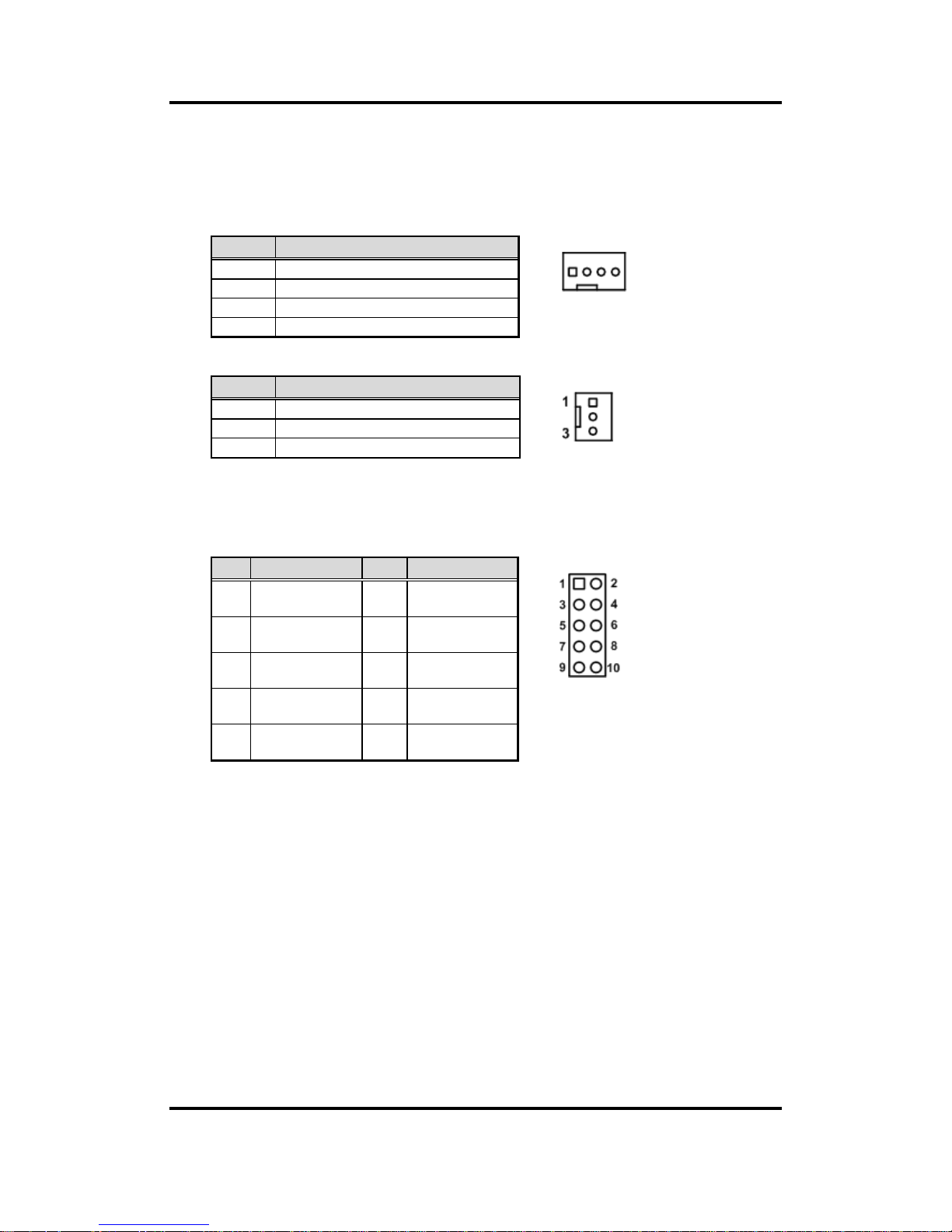
2.4.1 DisplayPort Combo Connector (CN3) ....................................................... 12
2.4.2 SIM Card Socket (CN5) ............................................................................ 12
2.4.3 mSATA Connector (CN6) .......................................................................... 13
2.4.4 SATA 3.0 Connectors (CN7~CN9) ............................................................ 13
2.4.5 Front Panel Header (CN12) ...................................................................... 14
2.4.6 USB 2.0 Port (CN13) ................................................................................. 15
2.4.7 USB 2.0 Wafer Connector (CN14) ............................................................ 15
2.4.8 ATX Power Input Connectors (CN16 and CN17) ...................................... 16
2.4.9 Fan Connectors (CN18 and CN19) ........................................................... 17
2.4.10 GPIO Header (CN20) ................................................................................ 17
2.4.11 COM D-Sub Connector (CN21) ................................................................ 18
2.4.12 COM Wafer Connectors (CN22 and CN23) .............................................. 18
2.4.13 LAN and USB 3.0 Connectors (CN26 and CN27) .................................... 19
2.4.14 Audio Jack (CN28) .................................................................................... 19
2.4.15 Front Audio Connector (CN29) .................................................................. 20
2.4.16 HDMI Connector (CN30) ........................................................................... 20
2.4.17 LVDS Signal Header (CN31) ..................................................................... 21
2.4.18 LVDS Backlight Control Header (CN32) ................................................... 22
Page 5

v
2.4.19 M.2 Key E Connector (CN34) ................................................................... 23
Chapter 3 Hardware Description ........................... 25
3.1 Microprocessors .................................................................................. 25
3.2 BIOS.................................................................................................... 25
3.3 System Memory .................................................................................. 25
Chapter 4 AMI BIOS Setup Utility .......................... 27
4.1 Starting ................................................................................................ 27
4.2 Navigation Keys .................................................................................. 27
4.3 Main Menu .......................................................................................... 29
4.4 Advanced Menu .................................................................................. 30
4.5 Chipset Menu ...................................................................................... 43
4.6 Security Menu ..................................................................................... 48
4.7 Boot Menu ................................ ................................ ........................... 49
4.8 Save & Exit Menu ................................................................................ 51
Appendix A Watchdog Timer ................................... 53
A.1 About Watchdog Timer ........................................................................ 53
A.2 Sample Program ................................................................................. 53
Page 6

vi
This page is intentionally left blank.
Page 7

MANO520 Mini ITX Motherboard
Introduction 1
Chapter 1
Introduction
The MANO520 Mini-ITX motherboard supports the new 14nm 8th Generation Intel® Core™ i7/
i5/ i3, Pentium® and Celeron
®
processors in LGA1151 package. Featuring the new Intel® H310
Express chipset with two DDR4 2666MHz memory support, this motherboard is built to
perform best stability and reliability for industrial applications.
It comes with three SATA 3.0, four USB 3.0, four USB 2.0 and one RS-232/422/485 port
providing robust storage and I/O options. Users also can increase board functionality with
PCI-Express x16 and mSATA slot. The high quality MANO520 allows four display interfaces
via HDMI, two DisplayPort and LVDS in quadruplicate views, making it an ideal solution for
gaming, workstation, digital signage, medical and other IoT&M2M applications.
1.1 Features
LGA1151 Socket for 8
th
Generation Intel® Core™ i7/ i5/ i3, Pentium® and Celeron®
processors (Coffee Lake)
2 DDR4 2666MHz memory with maximum capacity up to 32 GB
1 PCI-Express x16
1 mSATA and 1 SIM card slots (support SATA, USB 2.0 signal)
1 M.2 Key E, size: 22x30 for WiFi (support PCIE x1, USB 2.0 signal)
3 SATA-600
4 USB 3.0 and 4 USB 2.0
Page 8

MANO520 Mini ITX Motherboard
2 Introduction
1.2 Specifications
CPU
LGA1151 Socket for 8
th
Generation Intel® Core™ i7/ i5/ i3, Pentium® and Celeron®
processors.
Chipset
Intel
®
H310/Q370 (optional).
BIOS
AMI BIOS via SPI interface.
System Memory
Two 260-pin SO-DIMM sockets.
Maximum up to 32GB DDR4 memory.
Support 2666MHz.
Onboard Multi I/O
Controller: ITE8786.
Four serial ports:
- COM1 supports RS-232/422/485; COM2~COM4 support RS-232 only.
- COM1~COM2 on the rear I/O; COM3~COM4 in wafer connectors.
USB Interface
Four USB 3.0 ports (on the rear I/O).
Two USB 2.0 ports (on the rear I/O).
Two USB 2.0 ports in wafer connector (internal).
Ethernet
LAN1: 1000/100/10Mbps Gigabit/Fast Ethernet supports Wake-on-LAN, PXE with
Intel® i219LM.
LAN2: 1000/100/10Mbps Gigabit/Fast Ethernet supports Wake-on-LAN, PXE with
Intel® i211AT.
Serial ATA
Three SATA 3.0 port (6Gb/s).
One mSATA slot.
Audio
Realtek ALC662 5.1 channel HDA codec.
Support MIC-in/line-out (on the rear I/O).
Support MIC-in/line-out/line-in in box headers (internal).
Display
One HDMI with resolution max. up to 3840x2160 @30Hz.
Two DisplayPort++ with resolution max. up to 4096x2304 @60Hz.
One 24-bit dual channel LVDS and one 8-pin inverter connector. LVDS resolution is
max. up to 1920x1200.
Expansion Interface
One PCI-Express x16 slot.
One SIM card slot.
Page 9

MANO520 Mini ITX Motherboard
Introduction 3
Power Input
One ATX power input connector.
One 12V ATX power input connector for CPU power.
Operating Temperature
0°C ~ 60°C.
Storage Temperature
-10°C ~ 65°C.
Form Factor
Mini ITX (6.7” x 6.7”, 17.0cm x 17.0cm).
Note
All specifications and images are subject to change without notice.
1.3 Utilities Supported
Chipset driver
Graphics driver
Intel ME driver
Ethernet driver
Audio driver
Chipset_serialio driver
Intel_Rapid_Storage_Technology driver
Page 10
MANO520 Mini ITX Motherboard
4 Introduction
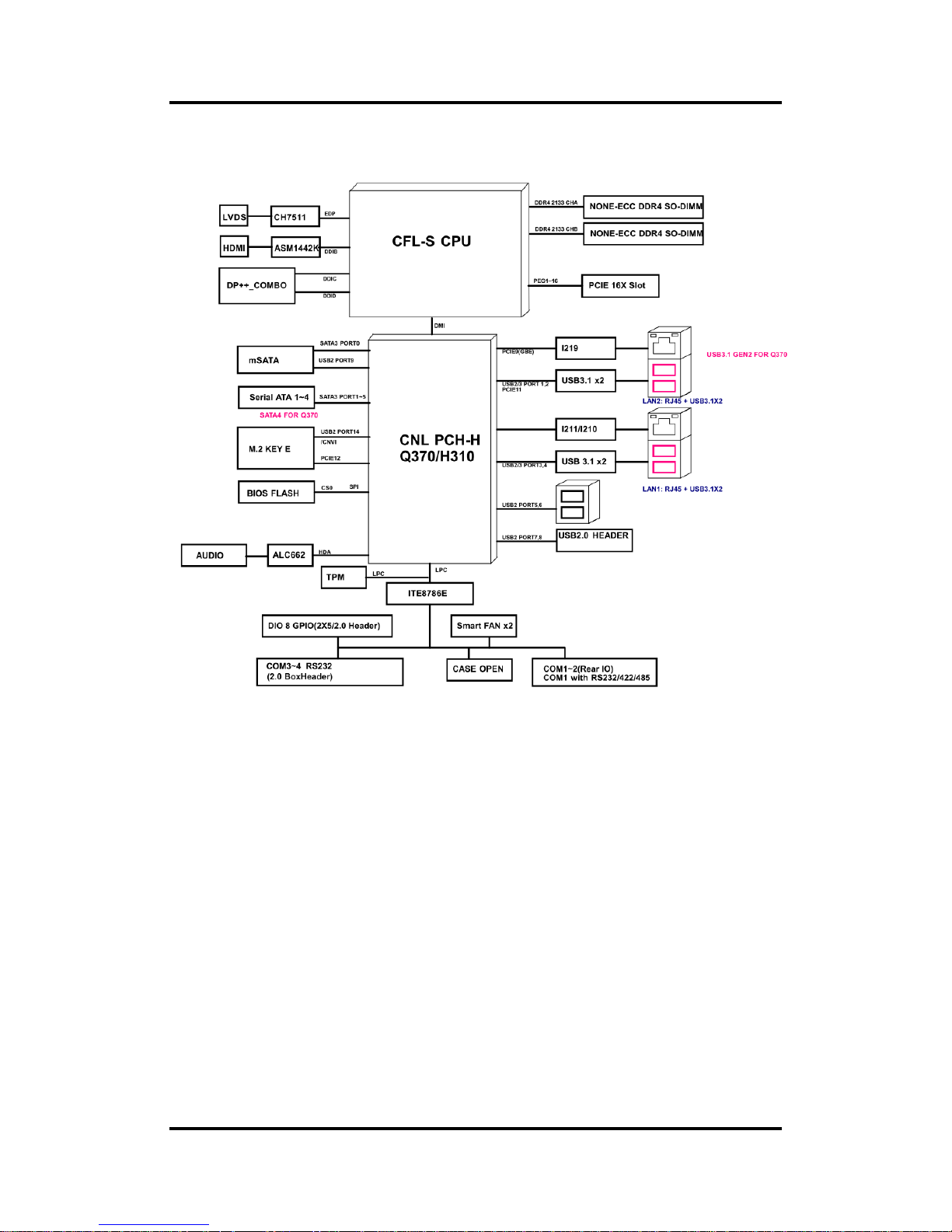
1.4 Block Diagram
Page 11

MANO520 Mini ITX Motherboard
Board and Pin Assignments 5
Chapter 2
Board and Pin Assignments
2.1 Board Layout
Page 12
MANO520 Mini ITX Motherboard
6 Board and Pin Assignments
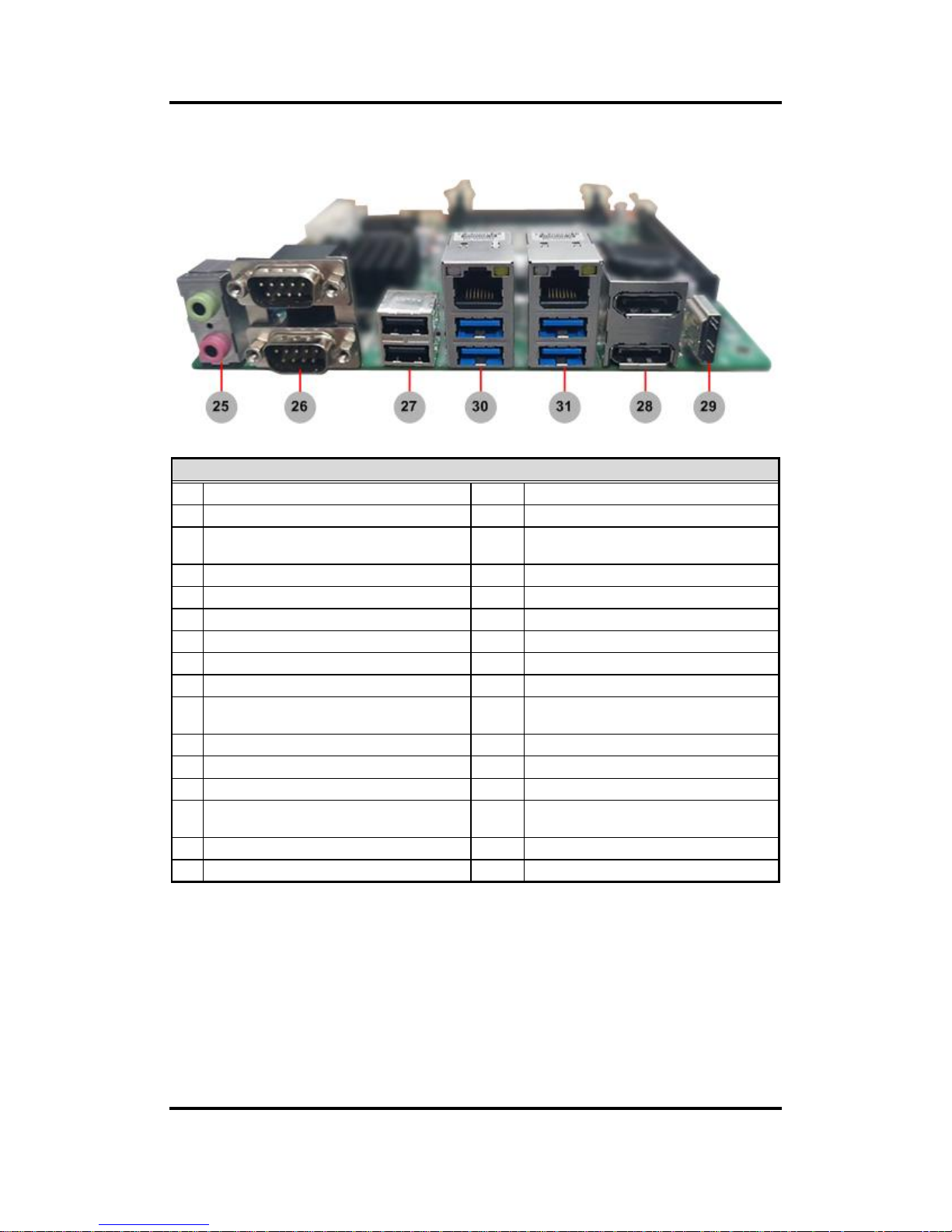
2.2 Rear I/O
Jumpers/Headers/Connectors
1
CPU Fan Connector (CN18)
17
Front Audio Connector (CN29)
2
4-pin ATX Power Input Connector (CN16)
18
COM1 Data/Power Select Jumper (JP5)
3
PCI-Express x16 Slot (CN15)
19
COM1 RS-232/422/485 Mode Select
Jumpers (JP4, JP6, JP7)
4
mSATA Connector (CN6)
20
Clear CMOS Jumper (JP1)
5
DDR4 SO-DIMM Connectors (CN1, CN2)
21
Case Open Select Jumper (JP10)
6
LVDS VDD Select Jumper (JP9)
22
GPIO Header (CN20)
7
LVDS Signal Header (CN31)
23
M.2 Key E Connector (CN34)
8
LVDS Backlight Control Header (CN32)
24
System Fan Connector (CN19)
9
SIM Card Socket (CN5)
25
Audio Jack (CN28)
10
LVDS Backlight PWM/DC Mode Select
Jumper (JP8)
26
COM1 and COM2 D-Sub Connector
(CN21)
11
24-pin ATX Power Input Connector (CN17)
27
USB 2.0 Port (CN13)
12
Front Panel Header (CN12)
28
DisplayPort Combo Connector (CN3)
13
AT/ATX Power Mode Select Jumper (JP3)
29
HDMI Connector (CN30)
14
COM3~COM4 Wafer Connectors (CN22,
CN23)
30
LAN1 and USB 3.0 Connector (CN26)
15
SATA 3.0 Connectors (CN7~CN9)
31
LAN2 and USB 3.0 Connector (CN27)
16
USB 2.0 Wafer Connector ( CN14)
Page 13
MANO520 Mini ITX Motherboard
Board and Pin Assignments 7
Note
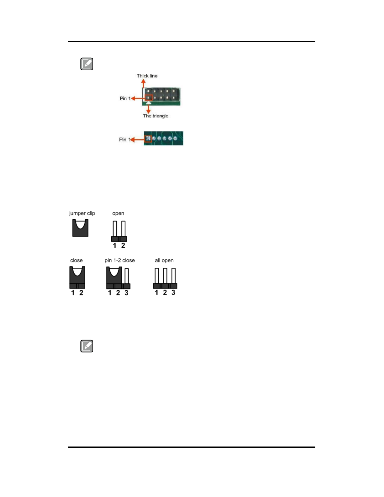
To identify the first pin of a header or jumper, please refer to the following
information:
Usually, there is a thick line or a triangle near the header or jumper pin 1.
Square pad, which you can find on the back of the motherboard, is usually
used for pin 1.
2.3 Jumper Settings
Jumper is a small component consisting of jumper clip and jumper pins. Install jumper clip on 2
jumper pins to close. And remove jumper clip from 2 jumper pins to open. The following
illustration shows how to set up jumper.
Before applying power to MANO520 Series, please make sure all of the jumpers are in factory
default position. Below you can find a summary table of all jumpers and onboard default
settings.
Note
Once the default jumper setting needs to be changed, please do it under power-off
condition.
Page 14

MANO520 Mini ITX Motherboard
8 Board and Pin Assignments
Jumper
Description
Setting
JP1
Clear CMOS
Default: Normal Operation
1-2 Close
JP3
AT/ATX Power Mode Select
Default: ATX Mode
1-2 Close
JP4
COM1 RS-232/422/485 Mode Select
Default: RS-232
1-2 Close
JP6
3-5, 4-6 Close
JP7
3-5, 4-6 Close
JP5
COM1 Data/Power Select
Default: RS-232 Data
CN21 Pin 1: DCD#
3-5 Close
CN21 Pin 9: RI#
4-6 Close
JP8
LVDS Backlight PWM/DC Mode Select
Default: PWM
1-2 Close
JP9
LVDS VDD Select
Default: +3.3V
1-2 Close
JP10
Case Open Select
Default: Close
1-2 Close
2.3.1 Clear CMOS (JP1)
This jumper allows you to clear the Real Time Clock (RTC) RAM in CMOS. You can
clear the CMOS memory of date, time, and system setup parameters by erasing the
CMOS RTC RAM data. The onboard button cell battery powers the RAM data in CMOS,
which includes system setup information such as system passwords.
To erase the RTC RAM:
1. Turn OFF the computer and unplug the power cord.
2. Remove the onboard battery.
3. Move the jumper clip from pins 1-2 (default) to pins 2-3. Keep the clip on pins 2-3
for about 5~10 seconds, then move the clip back to pins 1-2.
4. Re-install the battery.
5. Plug the power cord and turn ON the computer.
6. Hold down the <Del> key during the boot process and enter BIOS setup to re-enter
data.
2.3.2 AT/ATX Power Mode Select (JP3)
This 3-pin (pitch=2.0mm) jumper allows you to select AT or ATX power mode.
Function
Setting
Normal operation (Default)
1-2 close
Clear CMOS
2-3 close
Function
Setting
ATX mode (Default)
1-2 close
AT mode
2-3 close
Page 15

MANO520 Mini ITX Motherboard
Board and Pin Assignments 9
2.3.3 COM1 RS-232/422/485 Mode Select (JP4, JP6, JP7)
These are 3x2-pin (pitch=2.0mm) jumpers for setting COM1 port to operate in RS-232,
RS-422 or RS-485 communication mode.
JP4 JP6 JP7
2.3.4 COM1 Data/Power Select (JP5)
This is a 3x2-pin (pitch=2.0mm) jumper. The COM1 port has +5V power capability on
DCD and +12V on RI by setting JP5.
2.3.5 LVDS Backlight PWM/DC Mode Select (JP8)
This 3-pin (pitch=2.0mm) jumper enables you to select PWM or voltage control mode for
LVDS backlight control header (CN32). These two control modes are for adjusting the
brightness of LVDS panel.
2.3.6 LVDS VDD Select (JP9)
The motherboard supports voltage selection for flat panel displays. Use this 3x2-pin
(pitch=2.54mm) jumper to set up VDD power of the LVDS connector. To prevent
hardware damage, before connecting please make sure that the input voltage of LVDS
panel is correct.
Function
Setting
RS-232 mode
(Default)
JP4 1-2 close
JP6 3-5, 4-6 close
JP7 3-5, 4-6 close
RS-422 mode
JP4 3-4 close
JP6 1-3, 2-4 close
JP7 1-3, 2-4 close
RS-485 mode
JP4 5-6 close
JP6 1-3, 2-4 close
JP7 1-3, 2-4 close
Function
Setting
Power: Set COM1 pin 1 to +5V
1-3 close
Data: Set COM1 pin 1 to DCD (Default)
3-5 close
Power: Set COM1 pin 9 to +12V
2-4 close
Data: Set COM1 pin 9 to RI (Default)
4-6 close
Function
Setting
Controlled by PWM (Default)
1-2 close
Controlled by DC Voltage
2-3 close
Function
Setting
+3.3V (Default)
1-2 close
+5V
3-4 close
+12V
5-6 close
Page 16

MANO520 Mini ITX Motherboard
10 Board and Pin Assignments
2.3.7 Case Open Select (JP10)
The motherboard has one 2-pin (pitch=2.54mm) jumper for chassis intrusion detection
feature.
Function
Setting
Close (Default)
1-2 close
Active case open
1-2 open
Page 17

MANO520 Mini ITX Motherboard
Board and Pin Assignments 11
2.4 Connectors
Signals go to other parts of the system through connectors. Loose or improper connection
might cause problems, please make sure all connectors are properly and firmly connected.
Here is a summary table showing connectors on the hardware.
Connector
Description
CN1
DIMM1: DDR4 SO-DIMM Connector
CN2
DIMM2: DDR4 SO-DIMM Connector
CN3
DisplayPort Combo Connector
CN5
SIM Card Socket
CN6
mSATA Connector
CN7~CN9
SATA 3.0 Connectors
CN12
Front Panel Header
CN13
USB 2.0 port
CN14
USB 2.0 Wafer Connector
CN15
PCI-Express x16 Slot
CN16~CN17
ATX Power Input Connectors
CN18~CN19
Fan Connectors
CN20
GPIO Header
CN21
COM1 and COM2 D-Sub Connector
CN22~CN23
COM3 and COM4 Wafer Connectors
CN26~CN27
LAN and USB 3.0 Connectors
CN28
Audio Jack
CN29
Front Audio Connector
CN30
HDMI Connector
CN31
LVDS Signal Header
CN32
LVDS Backlight Control Header
CN34
M.2 Key E Connector
Page 18

MANO520 Mini ITX Motherboard
12 Board and Pin Assignments
2.4.1 DisplayPort Combo Connector (CN3)
The motherboard comes with DisplayPort Combo interface on the rear I/O.
2.4.2 SIM Card Socket (CN5)
The CN5 is for inserting SIM Card which is mainly used in 3G/4G wireless network
application. In order to work properly, the SIM Card must be used together with 3G/4G
module which is inserted to CN6.
6 7 8
Pin
Signal
1
DP_TX0_P
2
GND
3
DP_TX0_N
4
DP_TX1_P
5
GND
6
DP_TX1_N
7
DP_TX2_P
8
GND
9
DP_TX2_N
10
DP_TX3_P
11
GND
12
DP_TX3_N
13
GND
14
GND
15
DP_AUXP
16
GND
17
DP_AUXN
18
DP_HPD
19
GND
20
+3.3V
Pin
Signal
Pin
Signal
1
PWR_UIM
6
DAT_UIM
2
REST_UIM
7
VPP_UIM
3
CLK_UIM
8
GND
1 2 3
Page 19
MANO520 Mini ITX Motherboard
Board and Pin Assignments 13
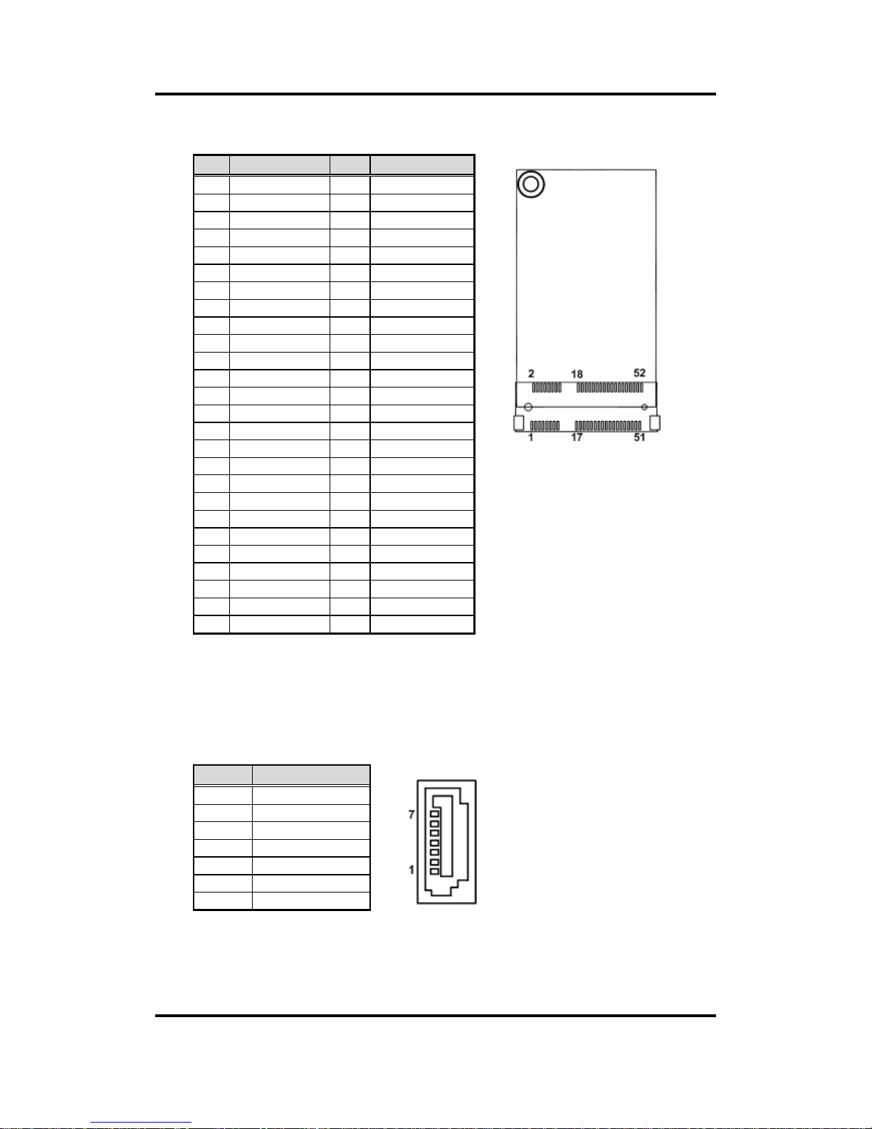
2.4.3 mSATA Connector (CN6)
2.4.4 SATA 3.0 Connectors (CN7~CN9)
These Serial Advanced Technology Attachment (Serial ATA or SATA) connectors are for
SATA 3.0 interfaces allowing up to 6.0Gb/s data transfer rate. They are computer bus
interfaces for connecting to devices such as hard disk drives.
Pin
Signal
Pin
Signal
1
N/C 2 +3.3VAUX
3
N/C 4 GND
5
N/C 6 +1.5V
7
N/C 8 UIM_PWR
9
GND
10
UIM_DAT
11
N/C
12
UIM_CLK
13
N/C
14
UIM_REST
15
GND
16
UIM_VPP
17
N/C
18
GND
19
N/C
20
N/C
21
GND
22
PERST#
23
SATA0_RX_DP
24
+3.3VAUX
25
SATA0_RX_DN
26
GND
27
GND
28
+1.5V
29
GND
30
SMB_CLK
31
SATA0_TX_DN
32
SMB_DATA
33
SATA0_TX_DP
34
GND
35
GND
36
USB#6_D-
37
GND
38
USB#6_D+
39
+3.3VAUX
40
GND
41
+3.3VAUX
42
N/C
43
GND
44
N/C
45
N/C
46
N/C
47
N/C
48
+1.5V
49
N/C
50
GND
51
N/C
52
+3.3VAUX
Pin
Signal
1
GND
2
SATA_TX+
3
SATA_TX-
4
GND
5
SATA_RX-
6
SATA_RX+
7
GND
Page 20

MANO520 Mini ITX Motherboard
14 Board and Pin Assignments
2.4.5 Front Panel Header (CN12)
The CN12 is a 7x2-pin (pitch=2.54mm) header for front panel interface.
Power LED
Pin 1 connects anode(+) of LED and pin 5 connects cathode(-) of LED. The power LED
lights up when the system is powered on.
External Speaker and Internal Buzzer
Pin 2, 4, 6 and 8 connect the case-mounted speaker unit or internal buzzer. While
connecting the board to an internal buzzer, please set pin 2 and 4 closed; while
connecting to an external speaker, you need to set pins 2 and 4 opened and connect the
speaker cable to pin 8(+) and pin 2(-).
Power On/Off Button
Pin 9 and 10 connect the power button on front panel to the board, which allows users to
turn on or off power supply.
System Reset Switch
Pin 11 and 12 connect the case-mounted reset switch that reboots your computer
without turning off the power switch. It is a better way to reboot your system for a longer
life of system power supply.
HDD Activity LED
This connection is linked to hard drive activity LED on the control panel. LED flashes
when HDD is being accessed. Pin 13 and 14 connect the hard disk drive to the front
panel HDD LED, pin 13 is assigned as cathode(-) and pin 14 is assigned as anode(+).
Pin
Signal
1
Power LED+
2
SPK-
3
GND
4
BUZZER-
5
Power LED-
6
N/C 7 N/C 8 SPK+
9
PWR-
10
PWR+
11
RESET-
12
RESET+
13
HD LED-
14
HD LED+
Page 21

MANO520 Mini ITX Motherboard
Board and Pin Assignments 15
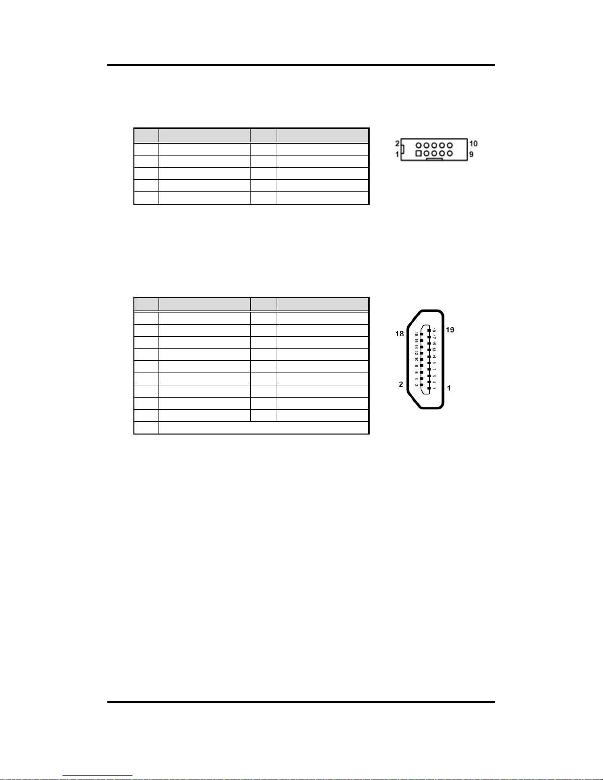
2.4.6 USB 2.0 Port (CN13)
The motherboard comes with one double-deck Universal Serial Bus (compliant with
USB 2.0 (480Mbps)) connector on the rear I/O for installing USB peripherals such as
keyboard, mouse, scanner, etc.
1 2 3 4
5 6 7 8
2.4.7 USB 2.0 Wafer Connector (CN14)
This is a 5x2-pin (pitch=2.00mm) connector for USB 2.0 interface.
Pin
Signal
Pin
Signal
1
USB VCC (+5V
level)
5
USB VCC (+5V
level)
2
USB #1_D-
6
USB #8_D-
3
USB #1_D+
7
USB #8_D+
4
GND
8
GND
Pin
Signal
Pin
Signal
1
+5V 2 +5V 3 USB#7_D-
4
USB#9_D-
5
USB#7_D +
6
USB#9_D +
7
GND
8
GND
10
N/C
Page 22

MANO520 Mini ITX Motherboard
16 Board and Pin Assignments
2.4.8 ATX Power Input Connectors (CN16 and CN17)
Steady and sufficient power can be supplied to all components on the board by
connecting power connector. Please make sure all components and devices are
properly installed before connecting the power connector.
External power supply plug fits into the connector in only one orientation. Properly press
down power supply plug until it completely and firmly fits into this connector. Loose
connection may cause system instability.
CN16 is a 4-pin connector for DC +12V power input.
2 4
1 3
CN17 is a 24-pin connector for DC power input.
Pin
Signal
1
GND
2
GND
3
+ 12V IN
4
+ 12V IN
Pin
Signal
Pin
Signal
1
3.3V
13
3.3V 2 3.3V
14
-12V
3
GND
15
GND
4
+5V
16
PS_ON
5
GND
17
GND
6
+5V
18
GND
7
GND
19
GND
8
PWR OK
20
-5V 9 5VSB
21
+5V
10
+12V
22
+5V
11
+12V
23
+5V
12
3.3V
24
GND
Page 23
MANO520 Mini ITX Motherboard
Board and Pin Assignments 17
2.4.9 Fan Connectors (CN18 and CN19)
The motherboard has two fan connectors. You can find fan speed option within BIOS
Setup Utility if fan is installed. For further information, see BIOS Setup Utility:
Advanced\Hardware Monitor\PC Health Status in section 4.4.
CN18: 4-pin (pitch=2.54mm)
1 4
CN19: 3-pin (pitch=2.54mm)
2.4.10 GPIO Header (CN20)
The CN20 is a 5x2-pin (pitch=2.00mm) header for GPIO interface.
Pin
Signal
1
GND
2
+12V
3
FAN Speed Detection
4
FAN Speed Control
Pin
Signal
1
GND
2
+12V
3
FAN Speed Detection
Pin
Signal
Pin
Signal
1
+5V
2
SIO_GPI70
(0xA06 Bit0, H)
3
SIO_GPO74
(0xA06 Bit4, H)
4
SIO_GPI71
(0xA06 Bit1, H)
5
SIO_GPO75
(0xA06 Bit5, H)
6
SIO_GPI72
(0xA06 Bit2, H)
7
SIO_GPO76
(0xA06 Bit6, H)
8
SIO_GPI73
(0xA06 Bit3, H)
9
SIO_GPO77
(0xA06 Bit7, H)
10
GND
Page 24

MANO520 Mini ITX Motherboard
18 Board and Pin Assignments
2.4.11 COM D-Sub Connector (CN21)
The CN21 is a double-deck D-Sub connector for COM1 and COM2 serial port interfaces
where only COM1 is selectable for RS-232/422/485 mode by jumper settings (see
section 2.3.3). The pin assignments of RS-232/422/485 are listed in table below.
COM1:
COM1
COM2
Note
[*]
: Pin 1 of COM1 can be DCD/+5V and pin 9 of COM1 can be RI/+12V by
selecting JP5 (see section 2.3.4).
COM2:
2.4.12 COM Wafer Connectors (CN22 and CN23)
The motherboard comes with two 5x2-pin (pitch=2.00mm) wafer connectors for COM3
and COM4 serial port interfaces.
Note
Cable is optional.
Pin
RS-232
RS-422
RS-485
1
DCD#
[*]
TX-
Data-
2
RXD
TX+
Data+
3
TXD
RX+
N/C 4 DTR#
RX-
N/C 5 GND
GND
GND
6
DSR#
N/C
N/C 7 RTS#
N/C
N/C 8 CTS#
N/C
N/C 9 RI#
[*]
N/C
N/C
Pin
Signal
Pin
Signal
1
DCD
2
RXD
3
TXD 4 DTR
5
GND
6
DSR
7
RTS 8 CTS 9 RI
Pin
Signal
Pin
Signal
1
DCD
2
DSR
3
RXD
4
RTS 5 TXD 6 CTS 7 DTR 8 RI 9 GND
10
N/C
Page 25

MANO520 Mini ITX Motherboard
Board and Pin Assignments 19
LAN1
USB
LAN2
USB
2.4.13 LAN and USB 3.0 Connectors (CN26 and CN27)
The motherboard comes with two high performance plug and play Ethernet interfaces
(RJ-45) which are fully compliant with the IEEE 802.3 standard. Connection can be
established by plugging one end of the Ethernet cable into this RJ-45 connector and the
other end to a 1000/100/10 Base-T hub.
The Universal Serial Bus (compliant with USB 3.0) connectors on the rear I/O are for
installing USB peripherals such as keyboard, mouse, scanner, etc.
CN26
Note
Speed LED turns orange for 1000Mbps or green for 100Mbps.
CN26/CN27 supports Wake-on-LAN. Only CN26 supports AMT when
chipset is customized into Intel® Q370.
CN27
2.4.14 Audio Jack (CN28)
The motherboard provides HD audio jack on the rear I/O. Install audio driver, and then
attach audio devices to CN28.
Pin
LAN Signal
Pin
LAN Signal
L1
Tx+ (Data
transmission positive)
L2
Tx- (Data transmission
negative)
L3
Rx+ (Data reception
positive)
L4
RJ-1 (For 1000 Base-T
only)
L5
RJ-1 (For 1000
Base-T only)
L6
Rx- (Data reception
negative)
L7
RJ-1 (For 1000
Base-T only)
L8
RJ-1 (For 1000 Base-T
only)
A
Active LED
B
Speed LED
Pin
USB Signal
Pin
USB Signal
1
USB3_POWER
2
USB -
3
USB +
4
GND
5
USB3_SSRX
6
USB3_SSRX+
7
GND
8
USB3_SSTX
9
USB3_SSTX+
Pin Color
Signal
Green
Line-out
Pink
MIC-in
Page 26
MANO520 Mini ITX Motherboard
20 Board and Pin Assignments
2.4.15 Front Audio Connector (CN29)
This is a 5x2-pin (pitch=2.00mm) connector for convenient connection and control of
audio devices.
2.4.16 HDMI Connector (CN30)
The HDMI (High-Definition Multimedia Interface) is a compact digital interface which is
capable of transmitting high-definition video and high-resolution audio over a single
cable.
Pin
Signal
Pin
Signal
1
MIC_IN
2
GND
3
LINE_IN_L
4
GND
5
LINE_IN_R
6
GND
7
AUD_OUT_L
8
GND
9
AUD_OUT_R
10
GND
Pin
Signal
Pin
Signal
1
HDMI OUT_DATA2+
2
GND
3
HDMI OUT_DATA2-
4
HDMI OUT_DATA1+
5
GND
6
HDMI OUT_DATA1-
7
HDMI OUT_DATA0+
8
GND
9
HDMI OUT_DATA0-
10
HDMI OUT_Clock+
11
GND
12
HDMI OUT_Clock-
13
N/C
14
GND
15
HDMI OUT_SCL
16
HDMI OUT_SDA
17
GND
18
+5V
19
HDMI_HTPLG
Page 27

MANO520 Mini ITX Motherboard
Board and Pin Assignments 21
2.4.17 LVDS Signal Header (CN31)
This is a 2x20-pin (pitch=1.0mm) connector which is compliant with JST
SM40B-SRDS-G-TF for LVDS LCD interface. It is strongly recommended to connect it
with matching connector, SHDR-40VS-B.
Note
[*]
: Panel power VDD is 3.3V by default, 5V or 12V is selectable by jumper
JP9, see section 2.3.6.
[**]
: Grounding of this pin is required to ensure normal LVDS output.
Pin
Signal
Pin
Signal
1
VDD
[*]
2
VDD
[*]
3
VDD
[*]
4
VDD
[*]
5
VDD
[*]
6
VDD
[*]
7
N/C 8 N/C 9 GND(Detect)
[**]
10
GND
11
LVDS_B_DATA3-
12
LVDS_B_DATA0-
13
LVDS_B_DATA3+
14
LVDS_B_DATA0+
15
GND
16
GND
17
LVDS_B_CLK-
18
LVDS_B_DATA1-
19
LVDS_B_ CLK +
20
LVDS_B_DATA1+
21
GND
22
GND
23
LVDS_A_DATA0-
24
LVDS_B_DATA2-
25
LVDS_A_DATA0+
26
LVDS_B_DATA2+
27
GND
28
GND
29
LVDS_A_DATA1-
30
LVDS_A_DATA3-
31
LVDS_A_DATA1+
32
LVDS_A_DATA3+
33
LVDS_PRSNT#
34
GND
35
LVDS_A_DATA2-
36
LVDS_A_CLK-
37
LVDS_A_DATA2+
38
LVDS_A_ CLK +
39
GND(Detect)
[**]
40
GND
Page 28
MANO520 Mini ITX Motherboard
22 Board and Pin Assignments
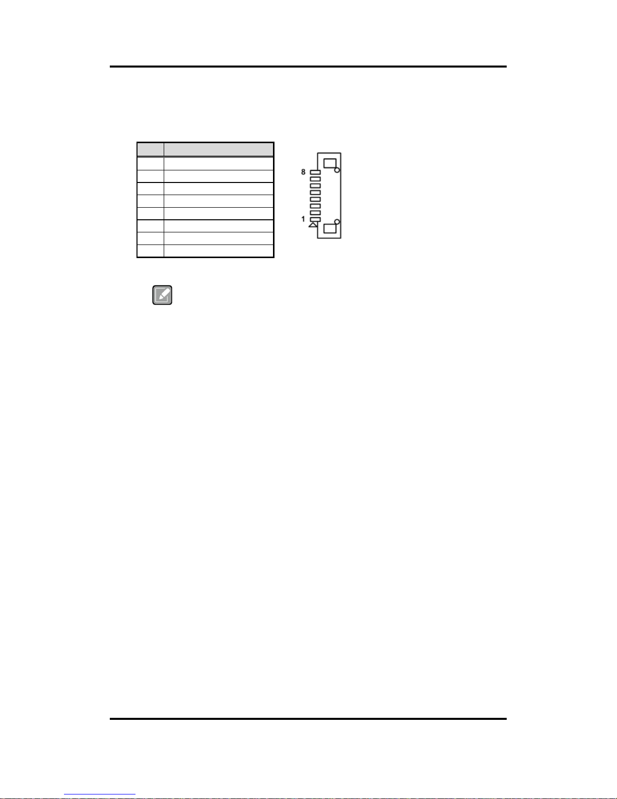
2.4.18 LVDS Backlight Control Header (CN32)
This is an 8-pin (pitch=1.25mm) connector which is compliant with Hirose
DF13-8P-1.25V for inverter. We strongly recommend you to use the matching connector,
DF13-8S-1.25C, to avoid malfunction.
Note
[*]
: This signal is selectable by jumper JP8, see section 2.3.5.
Pin
Signal
1
+12V
2
+12V
3
+5V 4 LVDS_BKL_EN
5
GND
6
GND
7
GND
8
LVDS_BKL_CTL
[*]
Page 29

MANO520 Mini ITX Motherboard
Board and Pin Assignments 23
2.4.19 M.2 Key E Connector (CN34)
The motherboard comes with one M.2 Key E connector (Wi-Fi & Bluetooth).
Note
[*]
: These pins are for CNVI module.
Pin
Signal
Pin
Signal
Pin
Signal
1
GND
26
N/C
51
GND 2 +3.3V
27
N/C
52
BUF_PLT_RST
3
USB#14_D+
28
N/C
53
NGFF_CLKREQ3
4
+3.3V
29
N/C
54
BT_KILL1
5
USB#14_D-
30
N/C
55
PCH_WAKE
6
N/C
31
N/C
56
WLAN_KILL1
7
GND
32
CNV_RGI_DT
[*]
57
GND 8 N/C
33
GND
58
N/C 9 CNV_WR_1_DN
[*]
34
CNV_RGI_RSP
[*]
59
CNV_WT_1_DN
[*]
10
PCM_CRF_RST
[*]
35
PCIE12_TX_DP
[*]
60
N/C
11
CNV_WR_1_DP
[*]
36
CNV_BRI_DT
[*]
61
CNV_WT_1_DP
[*]
12
N/C
37
PCIE12_TX_DN
62
N/C
13
GND
38
CL_RST
[*]
63
GND
14
PCMOUT_CLKREQ0
[*]
39
GND
64
M2_REFCLK
15
CNV_WR_0_DN
[*]
40
CL_DATA
[*]
65
CNV_WT_0_DN
[*]
16
N/C
41
PCIE12_RX_DP
66
N/C
17
CNV_WR_0_DP
[*]
42
CL_CLK
[*]
67
CNV_WT_0_DP
[*]
18
GND
43
PCIE12_RX_DN
68
N/C
19
GND
44
CNV_PA_BLANKING
[*]
69
GND
20
UART_BT_WAKE
[*]
45
GND
70
N/C
21
CNV_WR_CLK_DN
[*]
46
CNV_MFUART2_TXD
[*]
71
CNV_WT_CLK_DN
[*]
22
CNV_BRI_RSP
[*]
47
CLKOUT_PCIE_P3
72
+3.3V
23
CNV_WR_CLK_DP
[*]
48
CNV_MFUART2_RXD
[*]
73
CNV_WT_CLK_DP
[*]
24
N/C
49
CLKOUT_PCIE_N3
74
+3.3V
25
N/C
50
PCH_SUSCLK
75
GND
Page 30

MANO520 Mini ITX Motherboard
24 Board and Pin Assignments
This page is intentionally left blank.
Page 31

MANO520 Mini ITX Motherboard
Hardware Description 25
Chapter 3
Hardware Description
3.1 Microprocessors
The MANO520 Series supports Intel® Core™ i7/ i5/ i3, Pentium® and Celeron® processors,
which enable your system to operate under Windows® 10 and Linux environments. The
system performance depends on the microprocessor. Make sure all correct settings are
arranged for your installed microprocessor to prevent the CPU from damages.
3.2 BIOS
The MANO520 Series uses AMI Plug and Play BIOS with a single SPI Flash.
3.3 System Memory
The MANO520 supports two 260-pin DDR4 SO-DIMM sockets for maximum memory capacity
up to 32GB DDR4 SDRAMs. The memory module comes in sizes of 2GB, 4GB, 8GB and
16GB.
Note
For single memory channel configuration, install memory module in channel 0
(CN1) DDR4 SO-DIMM socket.
For dual memory channel configuration, install memory modules of the same
size, chip width, density and rank in both channel 0 (CN1) and channel 1 (CN2)
DDR4 SO-DIMM sockets.
Page 32

MANO520 Mini ITX Motherboard
26 Hardware Description
This page is intentionally left blank.
Page 33

MANO520 Mini ITX Motherboard
AMI BIOS Setup Utility 27
Chapter 4
AMI BIOS Setup Utility
The AMI UEFI BIOS provides users with a built-in setup program to modify basic system
configuration. All configured parameters are stored in a flash chip to save the setup information
whenever the power is turned off. This chapter provides users with detailed description about
how to set up basic system configuration through the AMI BIOS setup utility.
4.1 Starting
To enter the setup screens, follow the steps below:
1. Turn on the computer and press <Del> during the Power On Self Test (POST) to enter
BIOS setup, otherwise, POST will continue with its test routines.
2. Once you enter the BIOS, the main BIOS setup menu displays. You can access the other
setup screens from the main BIOS setup menu, such as the Advanced and Chipset
menus.
Note
If your computer cannot boot after making and saving system changes with BIOS
setup, you can restore BIOS optimal defaults by setting JP1 (see section 2.3.1).
It is strongly recommended that you should avoid changing the chipset’s defaults. Both AMI
and your system manufacturer have carefully set up these defaults that provide the best
performance and reliability.
4.2 Navigation Keys
The BIOS setup/utility uses a key-based navigation system called hot keys. Most of the BIOS
setup utility hot keys can be used at any time during the setup navigation process. These keys
include <F1>, <F2>, <Enter>, <ESC>, <Arrow> keys, and so on.
Note
Some of the navigation keys differ from one screen to another.
Page 34

MANO520 Mini ITX Motherboard
28 AMI BIOS Setup Utility
Hot Keys
Description
Left/Right
The Left and Right <Arrow> keys allow you to select a setup screen.
Up/Down
The Up and Down <Arrow> keys allow you to select a setup screen or sub
screen.
Enter
The <Enter> key allows you to display or change the setup option listed for a
particular setup item. The <Enter> key can also allow you to display the setup
sub screens.
+ Plus/Minus
The Plus and Minus <Arrow> keys allow you to change the field value of a
particular setup item.
F1
The <F1> key allows you to display the General Help screen.
F2
The <F2> key allows you to Load Previous Values.
F3
The <F3> key allows you to Load Optimized Defaults.
F4
The <F4> key allows you to save any changes you have made and exit Setup.
Press the <F4> key to save your changes.
Esc
The <Esc> key allows you to discard any changes you have made and exit the
Setup. Press the <Esc> key to exit the setup without saving your changes.
Page 35

MANO520 Mini ITX Motherboard
AMI BIOS Setup Utility 29
4.3 Main Menu
When you first enter the setup utility, you will enter the Main setup screen. You can always
return to the Main setup screen by selecting the Main tab. System Time/Date can be set up as
described below. The Main BIOS setup screen is shown below.
BIOS Information
Display the BIOS information.
System Date/Time
Use this option to change the system time and date. Highlight System Time or System Date
using the <Arrow> keys. Enter new values through the keyboard. Press the <Tab> key or the
<Arrow> keys to move between fields. The date must be entered in MM/DD/YY format. The
time is entered in HH:MM:SS format.
Access Level
Display the access level of current user.
Board Information
Display the board information.
Page 36
MANO520 Mini ITX Motherboard
30 AMI BIOS Setup Utility
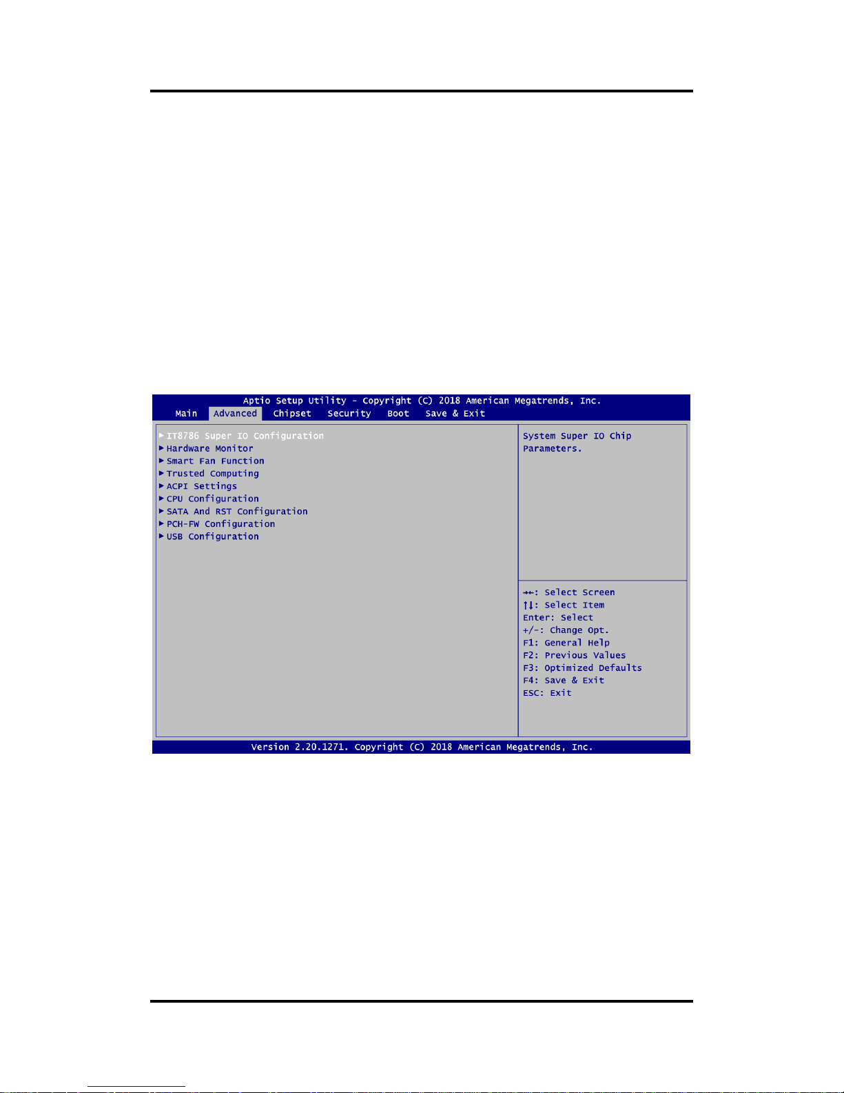
4.4 Advanced Menu
The Advanced menu also allows users to set configuration of the CPU and other system
devices. You can select any of the items in the left frame of the screen to go to the sub menus:
► IT8786 Super IO Configuration
► Hardware Monitor
► Smart Fan Function
► Trusted Computing
► ACPI Settings
► CPU Configuration
► SATA And RST Configuration
► PCH-FW Configuration
► USB Configuration
For items marked with “”, please press <Enter> for more options.
Page 37

MANO520 Mini ITX Motherboard
AMI BIOS Setup Utility 31
IT8786 Super IO Configuration
You can use this screen to select options for the Super IO Configuration, and change the
value of the selected option. A description of the selected item appears on the right side of
the screen. For items marked with “”, please press <Enter> for more options.
Serial Port 1~4 Configuration
Use these items to set parameters related to serial port 1~4.
Page 38

MANO520 Mini ITX Motherboard
32 AMI BIOS Setup Utility
Serial Port 1~4 Configuration
Serial Port
Enable or disable serial port 1~4. The optimal settings for base I/O address and for
interrupt request address are:
- Serial port 1: 3F8h, IRQ4
- Serial port 2: 2F8h, IRQ3
- Serial port 3: 3E8h, IRQ7
- Serial port 4: 2E8h, IRQ6
Page 39

MANO520 Mini ITX Motherboard
AMI BIOS Setup Utility 33
Hardware Monitor
This screen monitors hardware health status.
This screen displays the temperature of system and CPU, cooling fans speed in RPM and
system voltages (VCC_CPU, VCC_DDR, +12V, +5V and +3.3V standby).
Page 40

MANO520 Mini ITX Motherboard
34 AMI BIOS Setup Utility
Smart Fan Function
This screen allows you to select CPU fan and system fan mode.
CPU FAN\System FAN
This item allows you to select the fan speed option(s) of CPU fan and system fan (see
section 2.4.9) which can be set to Full on, Manual and Automatic Mode.
- Full On: The fan always runs at full speed.
- Manual Mode: Use the start PWM value to set fan speed manually. The range is from
0 to 255.
Page 41

MANO520 Mini ITX Motherboard
AMI BIOS Setup Utility 35
- Automatic Mode: Follow super I/O IT8786 integrated automatic mode described below
to adjust the fan speed.
Page 42
MANO520 Mini ITX Motherboard
36 AMI BIOS Setup Utility
Trusted Computing
This screen provides function for specifying the TPM settings.
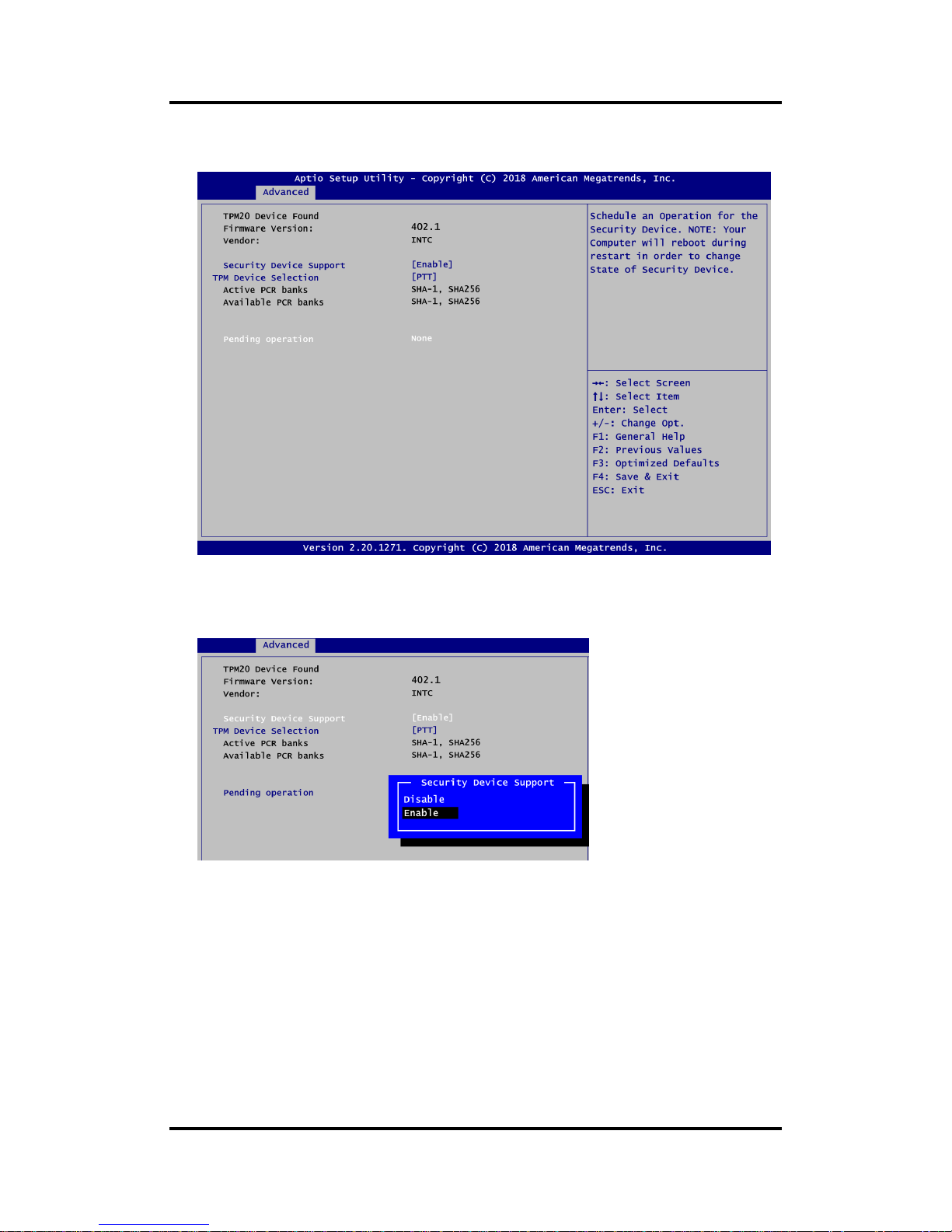
Security Device Support
Enable or disable BIOS support for security device, see image below. OS will not show
security device. TCG EFI protocol and INT1A interface will not be available.
Page 43

MANO520 Mini ITX Motherboard
AMI BIOS Setup Utility 37
TPM Device Selection
Select TPM device:
- PTT: Intel
®
built-in TPM.
- dTPM: External extended Infineon’s TPM (optional).
Pending operation
Schedule an operation for the security device, see image below.
- None
- TPM Clear: Clear all data secured by TPM.
Page 44

MANO520 Mini ITX Motherboard
38 AMI BIOS Setup Utility
ACPI Settings
ACPI Sleep State
When the suspend button is pressed, the ACPI (Advanced Configuration and Power
Interface) sleep state is S3 (Suspend to RAM).
Page 45
MANO520 Mini ITX Motherboard
AMI BIOS Setup Utility 39
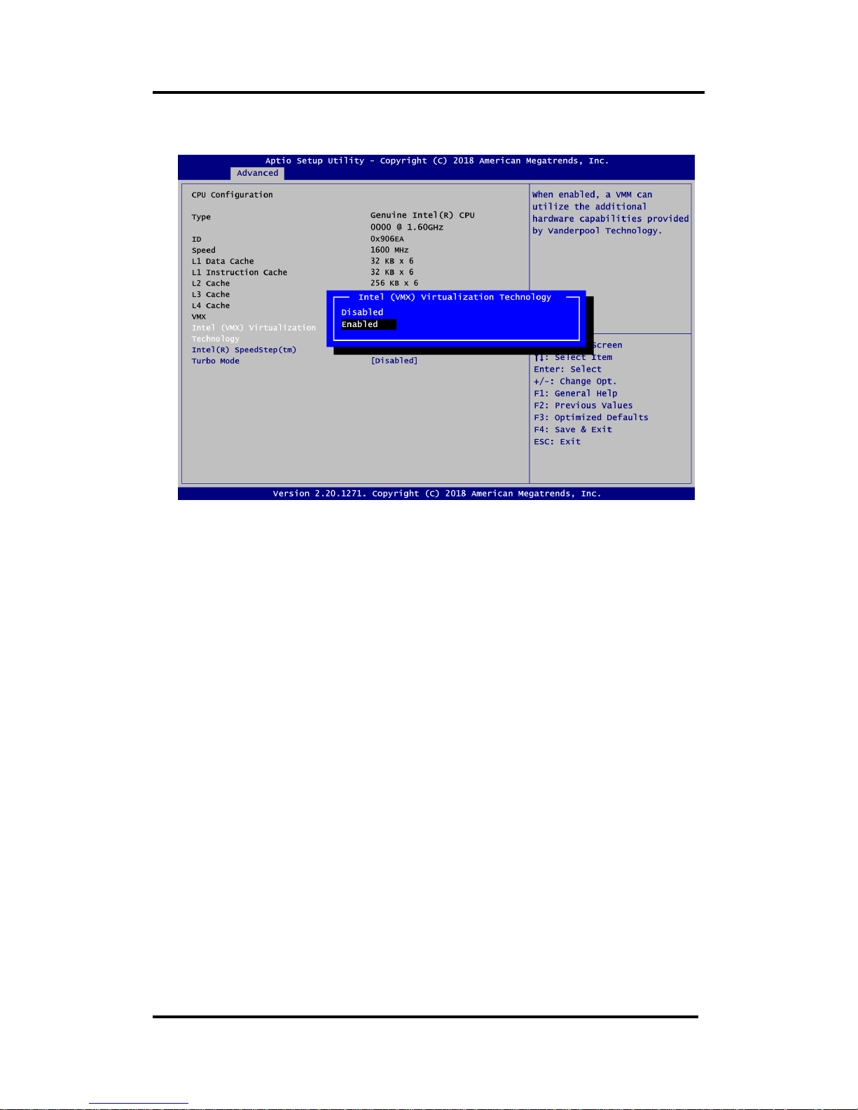
CPU Configuration
This screen shows CPU information, and you can change the value of the selected option.
Intel (VMX) Virtualization Technology
Enable or disable Intel Virtualization Technology. When enabled, a VMM (Virtual Machine
Mode) can utilize the additional hardware capabilities. It allows a platform to run multiple
operating systems and applications independently, hence enabling a single computer
system to work as several virtual systems.
Page 46
MANO520 Mini ITX Motherboard
40 AMI BIOS Setup Utility
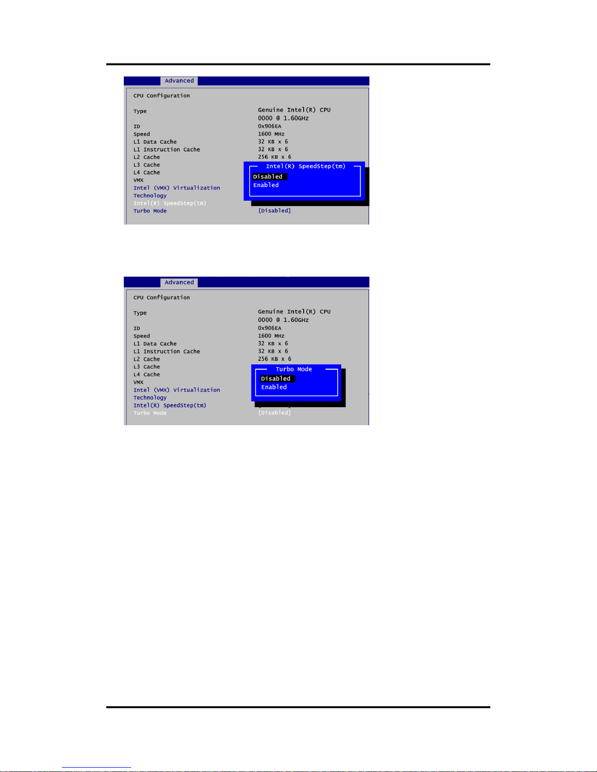
Intel(R) SpeedStep(tm)
Enable or disable Intel® SpeedStep. It allows more than two frequency ranges to be
supported.
Turbo Mode
Enable or disable Intel® turbo boost mode allowing processor cores to run faster but not
exceed CPU defined frequency limits.
Page 47
MANO520 Mini ITX Motherboard
AMI BIOS Setup Utility 41
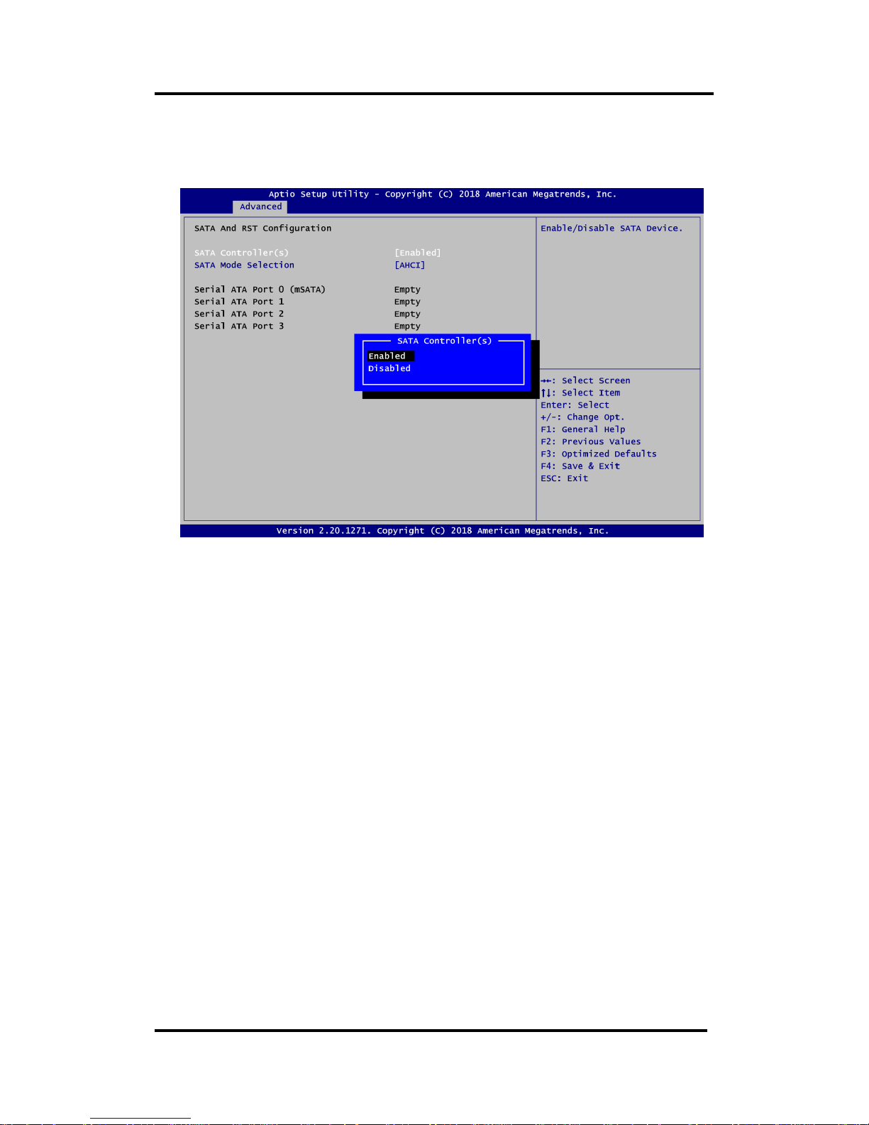
SATA and RST Configuration
During system boot up, BIOS automatically detects the presence of SATA devices. In the
SATA Configuration menu, you can see the currently installed hardware in the SATA
ports.
SATA Controller(s)
Enable or disable the SATA Controller feature. The default is Enabled.
SATA Mode Selection
Determine how SATA controller(s) operate. Operation mode options are:
- AHCI (Advanced Host Controller Interface)
- Intel RST Premium With Intel Optane System Acceleration
Page 48

MANO520 Mini ITX Motherboard
42 AMI BIOS Setup Utility
PCH-FW Configuration
This screen displays ME Firmware information.
USB Configuration
USB Devices
Display all detected USB devices.
Page 49

MANO520 Mini ITX Motherboard
AMI BIOS Setup Utility 43
4.5 Chipset Menu
The Chipset menu allows users to change the advanced chipset settings. You can select any
of the items in the left frame of the screen to go to the sub menus:
► System Agent (SA) Configuration
► PCH-IO Configuration
For items marked with “”, please press <Enter> for more options.
Page 50

MANO520 Mini ITX Motherboard
44 AMI BIOS Setup Utility
System Agent (SA) Configuration
This screen allows users to configure System Agent (SA) parameters. For items marked
with “”, please press <Enter> for more options.
Graphics Configuration
Open sub menu for parameters related to graphics configuration.
Memory Configuration
Open sub menu for information related to system memory.
Page 51
MANO520 Mini ITX Motherboard
AMI BIOS Setup Utility 45
Graphics Configuration
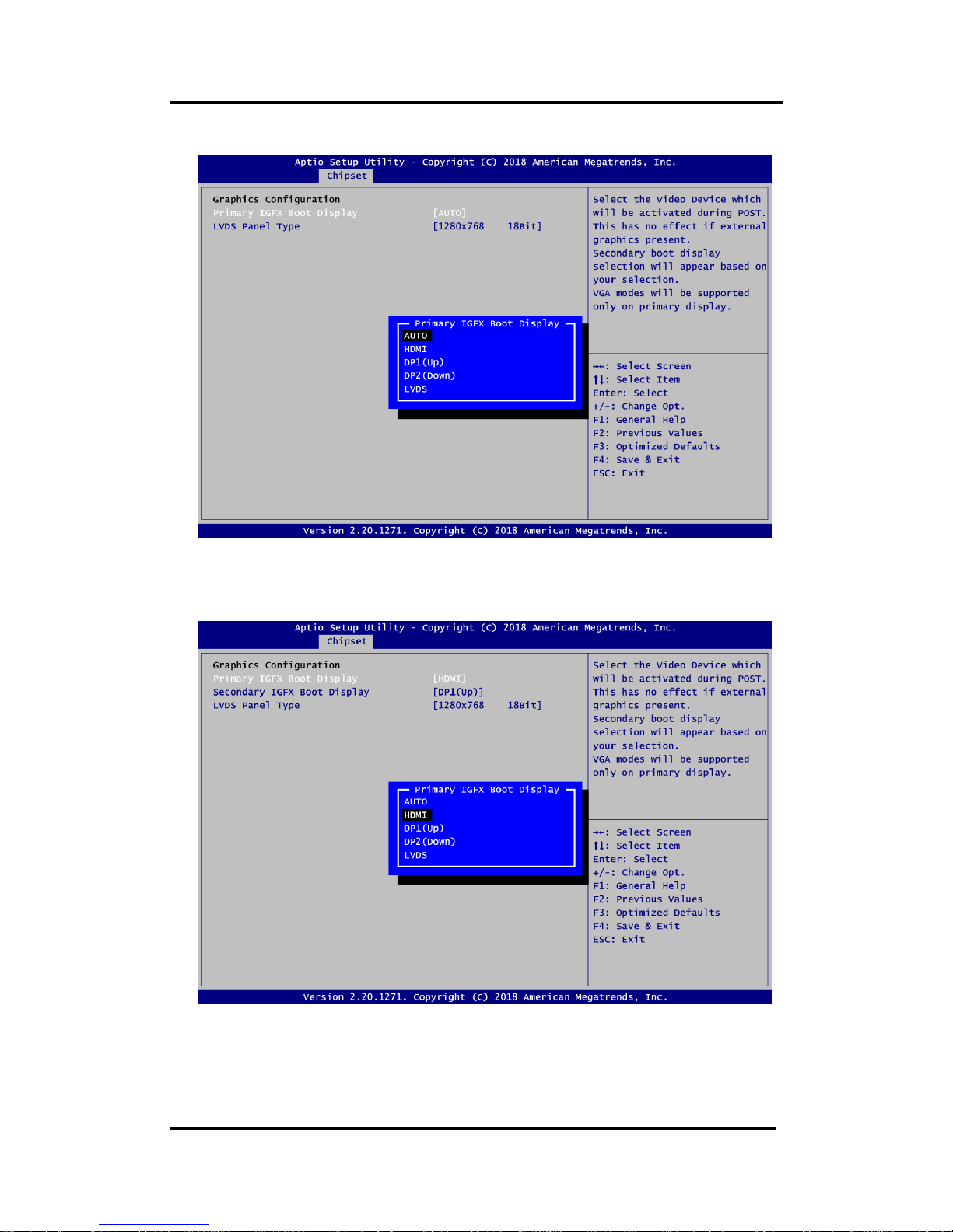
Primary IGFX Boot Display
Select the video device which will be activated during POST (Power-On Self Test). The
default is Auto.
Secondary IGFX Boot Display
After selecting other than “AUTO” on “Primary IGFX Boot Display”, the Secondary IGFX
Boot Display will show up and the options are Disabled, HDMI and VGA.
Page 52

MANO520 Mini ITX Motherboard
46 AMI BIOS Setup Utility
LVDS Panel Type
Select the appropriate LVDS panel resolution; see the selection options in image above.
Memory Configuration
This screen shows the system memory information.
Page 53
MANO520 Mini ITX Motherboard
AMI BIOS Setup Utility 47
PCH-IO Configuration
This screen allows you to set PCH parameters.
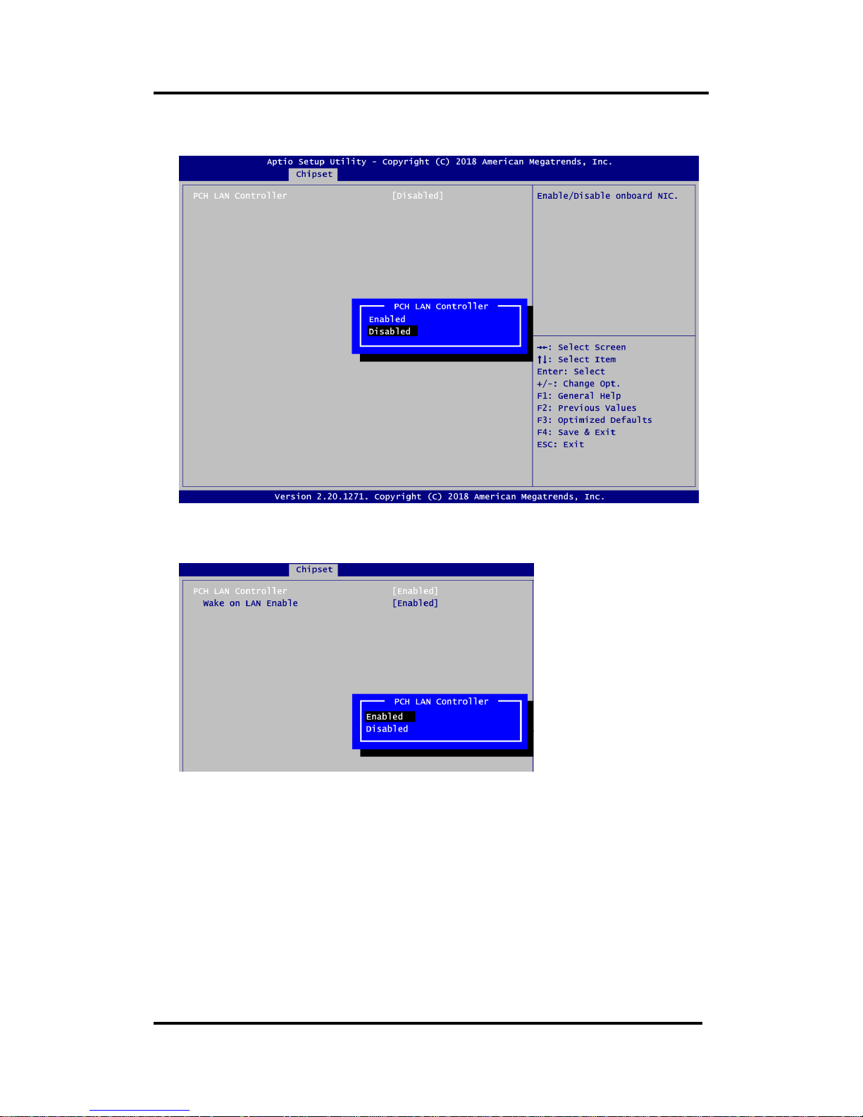
PCH LAN Controller
Enable or disable onboard PCH LAN controller.
Wake on LAN
After enabling PCH LAN Controller, enabling or disabling integrated LAN to wake the
system.
Page 54
MANO520 Mini ITX Motherboard
48 AMI BIOS Setup Utility
4.6 Security Menu
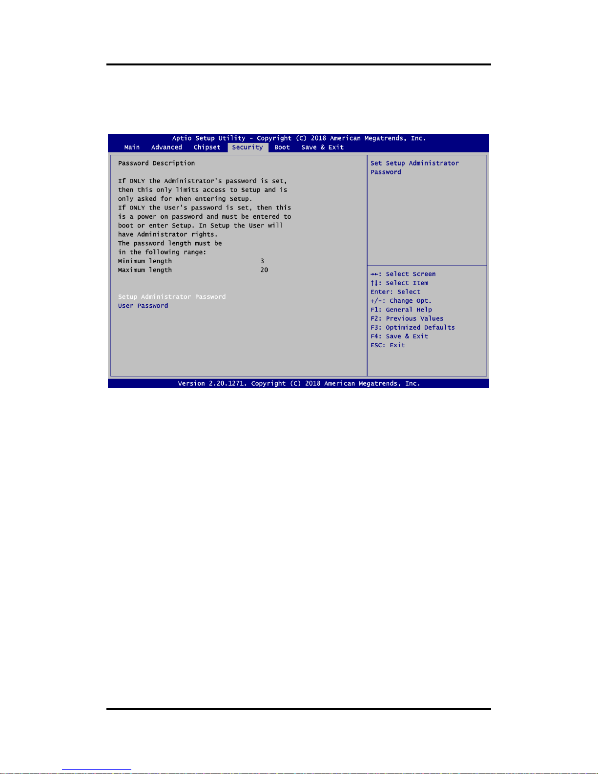
The Security menu allows users to change the security settings for the system.
Setup Administrator Password
Set setup administrator password.
User Password
Set user password.
Page 55

MANO520 Mini ITX Motherboard
AMI BIOS Setup Utility 49
4.7 Boot Menu
The Boot menu allows users to change boot options of the system.
Setup Prompt Timeout
Number of seconds to wait for setup activation key. 65535(0xFFFF) means indefinite
waiting.
Bootup NumLock State
Use this item to select the power-on state for the keyboard NumLock.
Quiet Boot
Select to display either POST output messages or a splash screen during boot-up.
Page 56

MANO520 Mini ITX Motherboard
50 AMI BIOS Setup Utility
Launch UEFI PXE OpROM policy
Control the execution of UEFI PXE OpROM. When enabled, you may select LAN1 or
LAN2 as PXE LAN port.
Boot Option Priorities
These are settings for boot priority. Specify the boot device priority sequence from the
available devices.
Boot Mode
Use this option for boot mode settings.
- UEFI Boot: Select support to boot any UEFI-capable OS.
- Legacy Boot: Select support to boot non UEFI-capable OS that expects a legacy BIOS
interface.
Page 57
MANO520 Mini ITX Motherboard
AMI BIOS Setup Utility 51
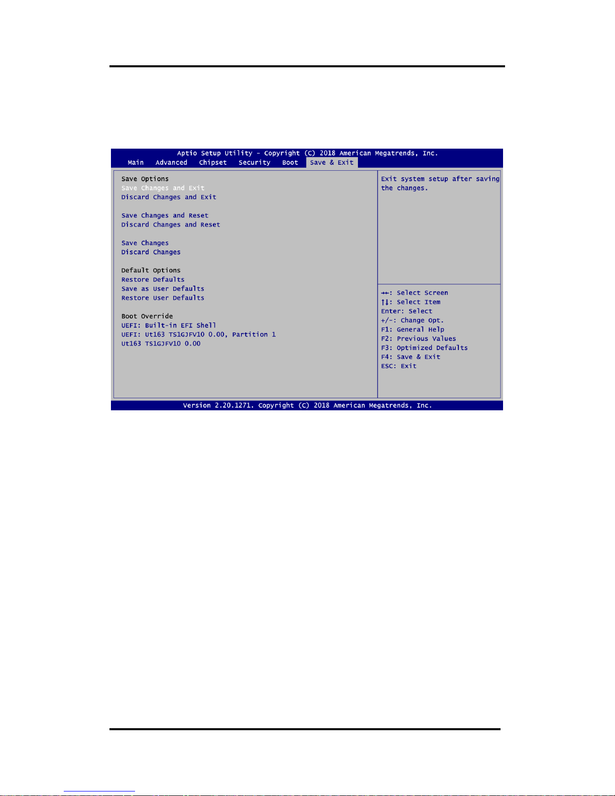
4.8 Save & Exit Menu
The Save & Exit menu allows users to load your system configuration with optimal or fail-safe
default values.
Save Changes and Exit
When you have completed the system configuration changes, select this option to leave
Setup and return to Main Menu. Select Save Changes and Exit from the Save & Exit menu
and press <Enter>. Select Yes to save changes and exit.
Discard Changes and Exit
Select this option to quit Setup without making any permanent changes to the system
configuration and return to Main Menu. Select Discard Changes and Exit from the Save &
Exit menu and press <Enter>. Select Yes to discard changes and exit.
Save Changes and Reset
When you have completed the system configuration changes, select this option to leave
Setup and reboot the computer so the new system configuration parameters can take
effect. Select Save Changes and Reset from the Save & Exit menu and press <Enter>.
Select Yes to save changes and reset.
Discard Changes and Reset
Select this option to quit Setup without making any permanent changes to the system
configuration and reboot the computer. Select Discard Changes and Reset from the Save
& Exit menu and press <Enter>. Select Yes to discard changes and reset.
Save Changes
When you have completed the system configuration changes, select this option to save
changes. Select Save Changes from the Save & Exit menu and press <Enter>. Select Yes
to save changes.
Page 58

MANO520 Mini ITX Motherboard
52 AMI BIOS Setup Utility
Discard Changes
Select this option to quit Setup without making any permanent changes to the system
configuration. Select Discard Changes from the Save & Exit menu and press <Enter>.
Select Yes to discard changes.
Restore Defaults
It automatically sets all Setup options to a complete set of default settings when you select
this option. Select Restore Defaults from the Save & Exit menu and press <Enter>.
Save as User Defaults
Select this option to save system configuration changes done so far as User Defaults.
Select Save as User Defaults from the Save & Exit menu and press <Enter>.
Restore User Defaults
It automatically sets all Setup options to a complete set of User Defaults when you select
this option. Select Restore User Defaults from the Save & Exit menu and press <Enter>.
Boot Override
Select a drive to immediately boot that device regardless of the current boot order.
Page 59

MANO520 Mini ITX Motherboard
Watchdog Timer 53
Appendix A
Watchdog Timer
A.1 About Watchdog Timer
Software stability is major issue in most application. Some embedded systems are not
watched by human for 24 hours. It is usually too slow to wait for someone to reboot when
computer hangs. The systems need to be able to reset automatically when things go wrong.
The watchdog timer gives us solution.
The watchdog timer is a counter that triggers a system reset when it counts down to zero from
a preset value. The software starts counter with an initial value and must reset it periodically. If
the counter ever reaches zero which means the software has crashed, the system will reboot.
A.2 Sample Program
1. Enter ADU, and press <F4> to select the superior ITE
2. PORT setting 002E, 002F
3. Address 07h setting 07 GPIO
4. Address 72h to set the countdown, for example Sec: C0, Min: 40
5. Address 73h set the countdown time, for example 10sec: 0A
 Loading...