

Page 1

CEM830 Series
®
Intel
Core™ 2 Duo
COM Express™ Type-II Module
User’s Manual
Page 2

Disclaimers
This manual has been carefully checked and believed to contain
accurate information. AXIOMTEK Co., Ltd. assumes no responsibility
for any infringements of patents or any third party’s rights, and any
liability arising from such use.
AXIOMTEK does not warrant or assume any legal liability or
responsibility for the accuracy, completeness or usefulness of any
information in this document. AXIOMTEK does not make any
commitment to update the information in this manual.
AXIOMTEK reserves the right to change or revise this document
and/or product at any time without notice.
No part of this document may be reproduced, stored in a retrieval
system, or transmitted, in any form or by any means, electronic,
mechanical, photocopying, recording, or otherwise, without the prior
written permission of AXIOMTEK Co., Ltd.
CAUTION
If you replace wrong batteries, it causes the danger of explosion. It is
recommended by the manufacturer that you follow the manufacturer’s
instructions to only replace the same or equivalent type of battery,
and dispose of used ones.
©Copyright 2008 AXIOMTEK Co., Ltd.
All Rights Reserved
June 2008, Version A4
Printed in Taiwan
ii
Page 3

ESD Precautions
Computer boards have integrated circuits sensitive to static electricity.
To prevent chipsets from electrostatic discharge damage, please take
care of the following jobs with precautions:
Do not remove boards or integrated circuits from their anti-static
packaging until you are ready to install them.
Before holding the board or integrated circuit, touch an unpainted
portion of the system unit chassis for a few seconds. It
discharges static electricity from your body.
Wear a wrist-grounding strap, available from most electronic
component stores, when handling boards and components.
Trademarks Acknowledgments
AXIOMTEK is a trademark of AXIOMTEK Co., Ltd.
Windows
Phoenix & AWARD are trademarks of Phoenix Technology Ltd.
IBM, PC/AT, PS/2, VGA are trademarks of International Business
Machines Corporation.
Intel
Winbond is a trademark of Winbond Electronics Corp.
Other brand names and trademarks are the properties and registered
brands of their respective owners.
®
is a trademark of Microsoft Corporation.
®
and Pentium® are trademarks of Intel Corporation.
iii
Page 4

Table of Contents
Disclaimers........................................................................................................... ii
ESD Precautions ................................................................................................. iii
Chapter 1 Introduction.................................................................... 1
1.1 Specifications.......................................................................................... 2
1.2 Utilities Supported................................................................................... 3
Chapter 2 Board Layout and Pin Assignments............................ 5
2.1 Board Dimensions and Fixing Holes....................................................... 5
2.2 Board Layout........................................................................................... 7
2.3 Pin Assignments...................................................................................... 9
Chapter 3 Hardware Description.................................................. 19
3.1 Microprocessors.................................................................................... 19
3.2 BIOS......................................................................................................19
3.3 System Memory..................................................................................... 19
3.4 I/O Port Address Map (With CEB94000 under WinXP)......................... 20
3.5 Interrupt Controller (With CEB94000 under WinXP)............................. 22
3.6 Memory Map (With CEB94000 under WinXP)...................................... 23
Chapter 4 Award BIOS Utility....................................................... 25
4.1 Entering Setup....................................................................................... 25
4.2 Control Keys..........................................................................................26
4.3 Getting Help .......................................................................................... 26
4.4 The Main Menu ..................................................................................... 27
4.5 Standard CMOS Setup Menu................................................................ 28
4.6 Advanced BIOS Features...................................................................... 31
4.7 Advanced Chipset Features.................................................................. 36
4.8 Integrated Peripherals........................................................................... 40
4.9 Power Management Setup.................................................................... 44
4.10 PnP/PCI Configuration Setup................................................................ 48
4.11 PC Health Status................................................................................... 50
4.12 Frequency/Voltage Control.................................................................... 51
4.13 Load Optimized Defaults....................................................................... 52
4.14 Set Supervisor/User Password ............................................................. 53
4.15 Save & Exit Setup ................................................................................. 54
4.16 Exit Without Saving............................................................................... 55
Appendix A Watchdog Timer ........................................................... 57
Appendix B
Appendix C
iv
GPIO & Watchdog Timer Programming Source Code.......... 59
Configuring SATA for RAID Function................................ 65
Page 5
CEM830 COM Express
TM
Type-II Module User’s Manual
C h a p t e r 1
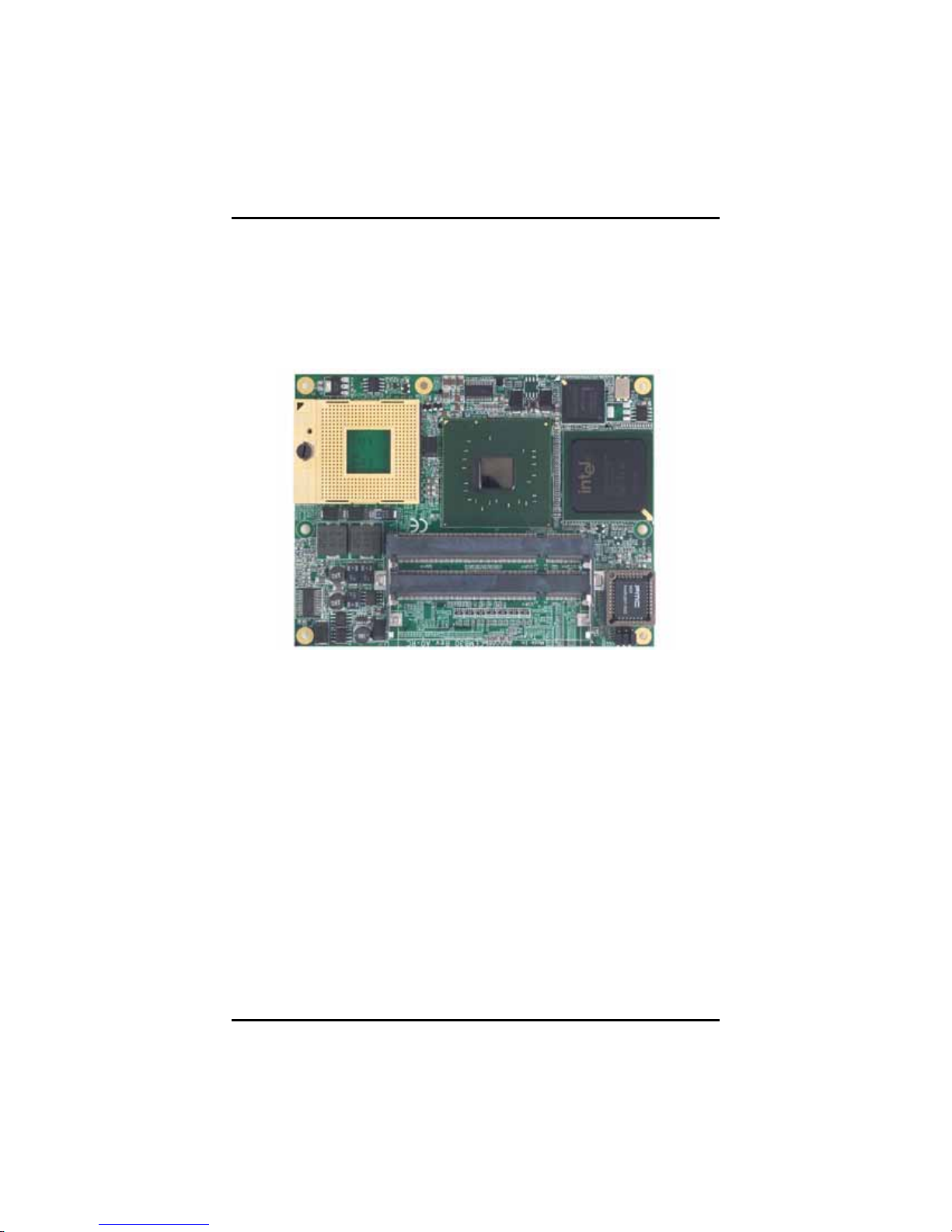
Introduction
The CEM830 is a new COM Express
®
Intel
CoreTM 2 Duo, CoreTM Duo, and Celeron
533/667MHz FSB. It is practically finest embedded Socket M (478-pin)
computer-on-module in the market. It integrates Intel
ICH7M chipsets, excellent Multiple I/O, LVDS LCD, Fast/Gigabit
Ethernet and AC'97/HD digital Audio interface to make all in one
single module as computing engine. It provides one PCI Express X16
for graphics or SDVO, PCI Express X1, 32-bit/33MHz PCI master
which are for expansion purpose.
This module supports various I/O features: CRT, LVDS LCD,
Fast/Gigabit Ethernet, HD Audio, PATA IDE, SATA IDE, USB 2.0,
GPIO and Watchdog timer.
Introduction
TM
Type-II Module to support
®
M processors with
®
945GME &
1
Page 6

CEM830 COM ExpressTM Type-II Module User’s Manual
1.1 Specifications
z CPU: Socket M (478-pin) for Intel
and Celeron
z System Chipset: Intel
z CPU Frequency: 533/667MHz FSB
z BIOS
Phoenix-Award BIOS, Y2K compliant
4Mbit Flash, DMI, Plug and Play
SmartView for multiple LCD type selection, display
®
M processors
®
945GME & ICH7M
mode option and application extension features
“Load Optimized Default” to backup customized Setting in
the BIOS flash chip to prevent from CMOS battery fail
z System Memory
Two x 200-pin DDR2 SO-DIMM sockets
Maximum to 4GB DDR2 memory (Intel 945GME supports
DDR2-400/533/667 up to 4GB, the actual maximum
capacity will be less depending on system configuration)
z L2 Cache: integrated in CPU
®
CoreTM 2 Duo, CoreTM Duo,
z USB Interface
Eight USB ports with fuse protection and complies with
USB Spec. Rev. 2.0
z Graphics:
Intel
CRT and LVDS LCD output
Maximum up to 224MB frame buffer sharing system
®
945GME GMCH Gen 3.5 integrated graphic engine
memory
Maximum display resolution:
CRT: 2048 x1536
LVDS: 1920 X1200 (18 or 24-bit
single/dual channel LVDS interface)
z Expansion Interface:
One PCI Express X16 interface for SDVO ADD2+ Card as
default (PCI Express X16 for discrete graphics is optional
2
Introduction
Page 7

CEM830 COM Express
TM
Type-II Module User’s Manual
with on-board LVDS function removal)
Four PCI Express X1 interface (CEM830VE version)
Three PCI Express X1 interface (CEM830VG version)
Four 32-bit/33MHz PCI master
z Ethernet:
Intel
z Audio:
HD Audio
z Power Management:
ACPI (Advanced Configuration and Power Interface)
®
i82562GZ for PCI-E Fast Ethernet and optional with
co-layout as Intel
®
i82573V for Gigabit Ethernet
NOTE All specifications and images are subject to change
without notice.
1.2 Utilities Supported
z Chipset Driver
z VGA Driver
z Ethernet Driver
z Audio Driver
z RAID Driver
Introduction
3
Page 8

CEM830 COM ExpressTM Type-II Module User’s Manual
MEMO
4
Introduction
Page 9
CEM830 COM Express
TM
Type-II Module User’s Manual
C h a p t e r 2
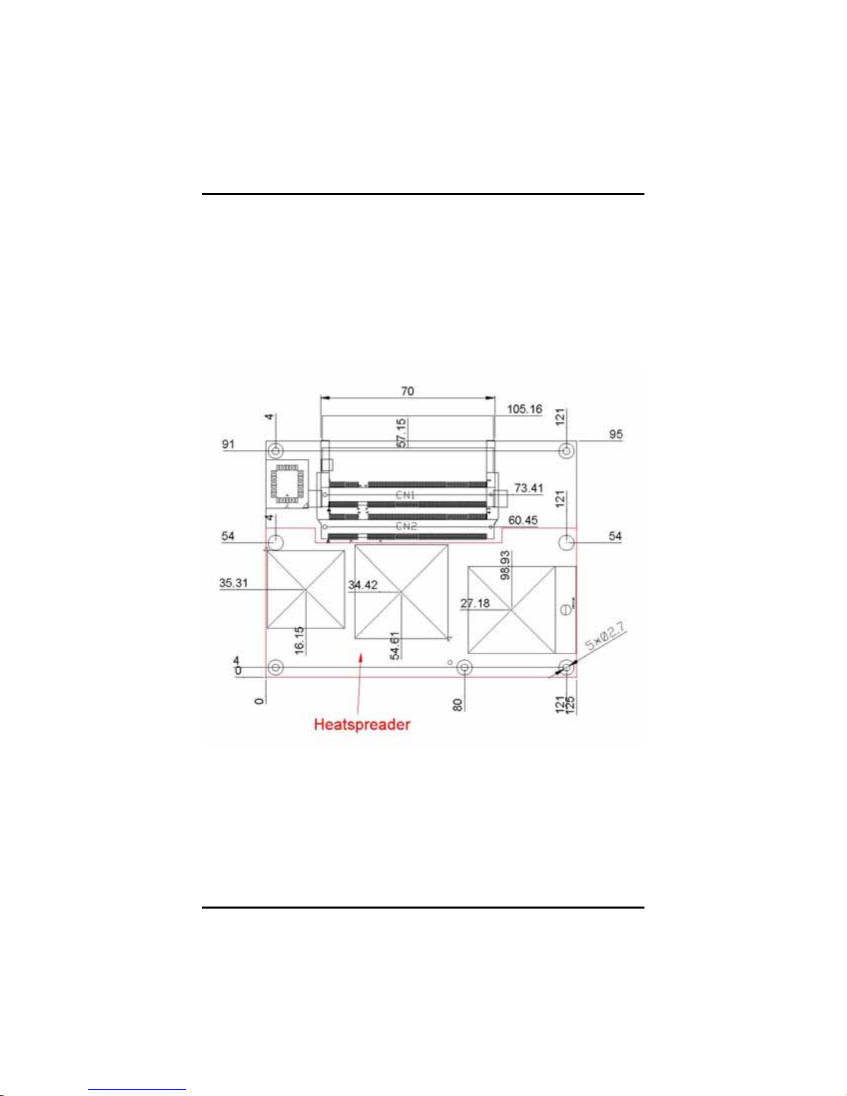
Board Layout and Pin Assignments
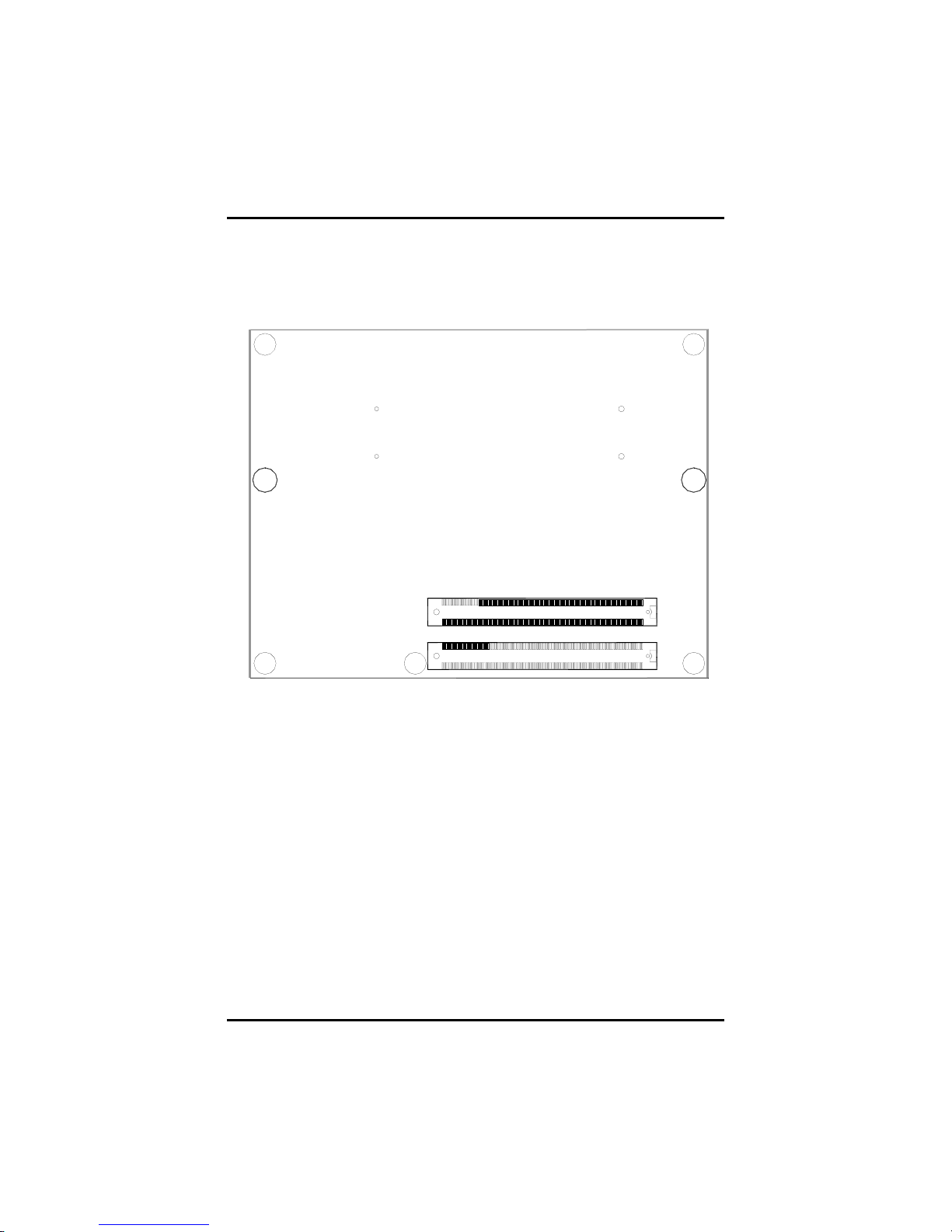
2.1 Board Dimensions and Fixing Holes
Jumpers and Connectors
Component Side
5
Page 10
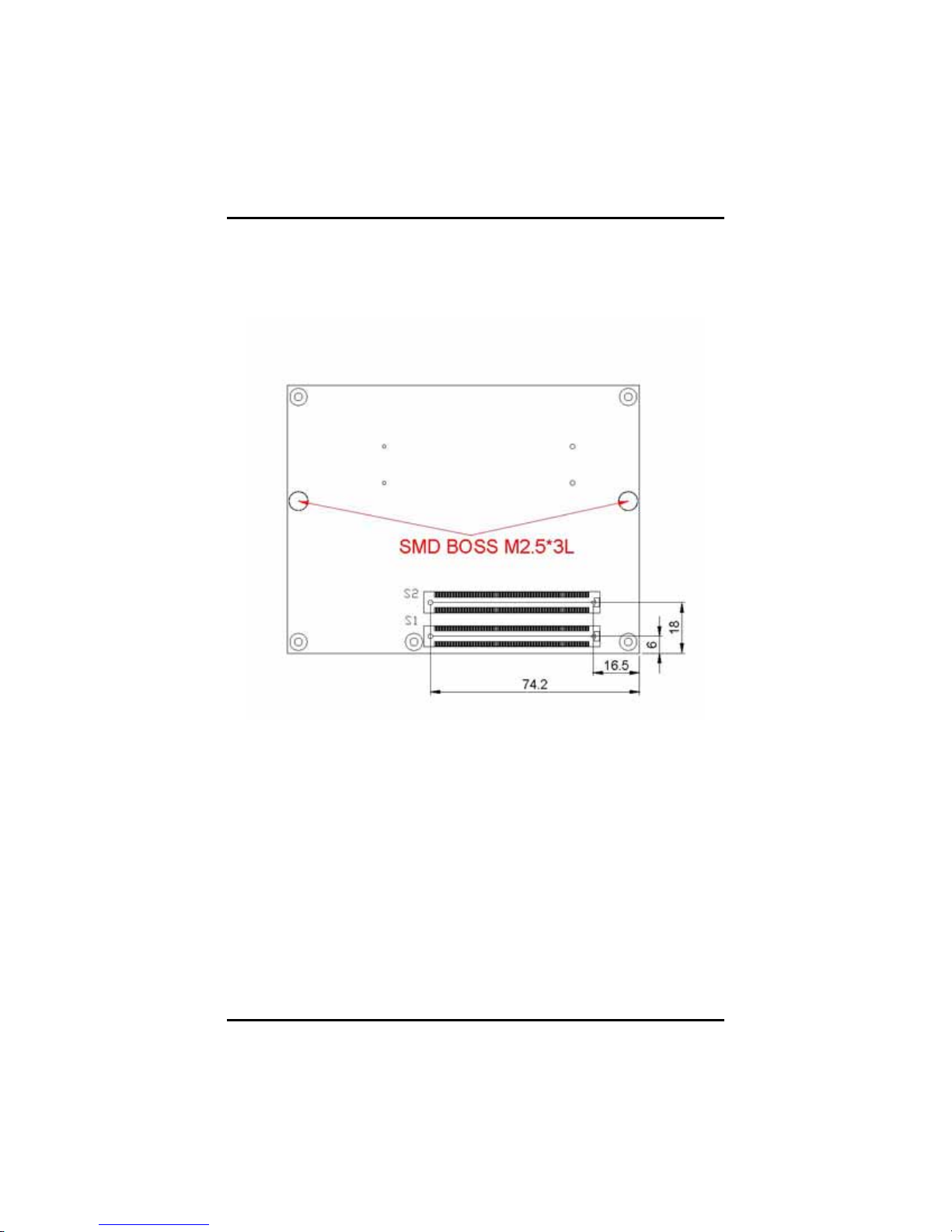
CEM830 COM ExpressTM Type-II Module User’s Manual
6
Solder Side
Jumpers and Connectors
Page 11
CEM830 COM Express
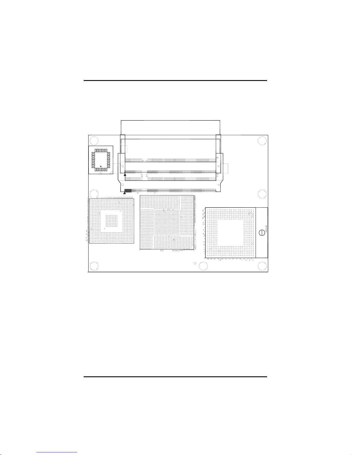
2.2 Board Layout
CN1
CN2
TM
Type-II Module User’s Manual
U8
Jumpers and Connectors
Component Side
7
Page 12
CEM830 COM ExpressTM Type-II Module User’s Manual
S2
S1
8
Solder Side
Jumpers and Connectors
Page 13
CEM830 COM Express
TM
Type-II Module User’s Manual
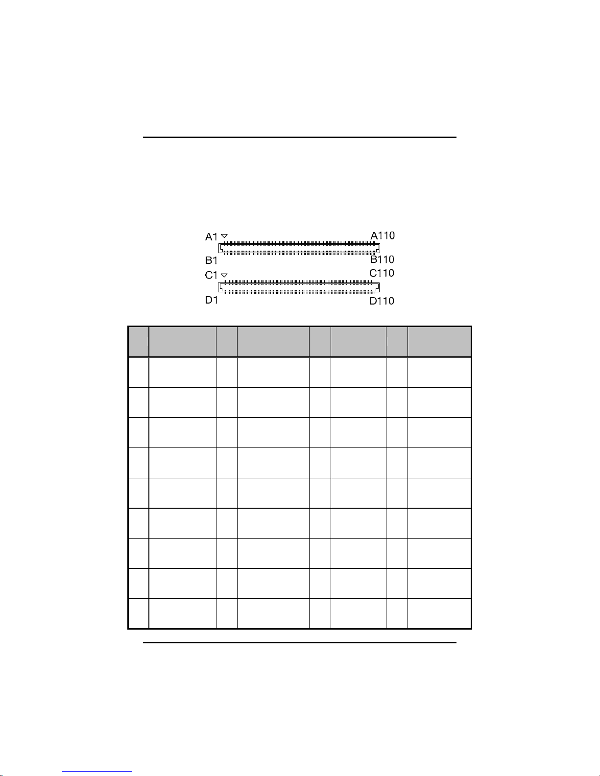
2.3 Pin Assignments
S1, S2:COM ExpressTM Connector
Pin Description Pin Description Pin Description Pin Description
A1 GND (FIXED) B1 GND (FIXED) C1 GND (FIXED) D1 GND (FIXED)
A2 GBE0_MDI3- B2 GBE0_ACT# C2 IDE_D7 D2 IDE_D5
A3 GBE0_MDI3+ B3 LPC_FRAME# C3 IDE_D6 D3 IDE_D10
A4 GBE0_LINK100# B4 LPC_AD0 C4 IDE_D3 D4 IDE_D11
A5 GBE0_LINK1000# B5 LPC_AD1 C5 IDE_D15 D5 IDE_D12
A6 GBE0_MDI2- B6 LPC_AD2 C6 IDE_D8 D6 IDE_D4
A7 GBE0_MDI2+ B7 LPC_AD3 C7 IDE_D9 D7 IDE_D0
A8 GBE0_LINK# B8 LPC_DRQ0# C8 IDE_D2 D8 IDE_REQ
A9 GBE0_MDI1- B9 LPC_DRQ1# C9 IDE_D13 D9 IDE_IOW#
Jumpers and Connectors
9
Page 14

CEM830 COM ExpressTM Type-II Module User’s Manual
Pin Description Pin Description Pin Description Pin Description
A10 GBE0_MDI1+ B10 LPC_CLK C10 IDE_D1 D10 IDE_ACK#
A11 GND (FIXED) B11 GND (FIXED) C11 GND (FIXED) D11 GND (FIXED)
A12 GBE0_MDI0- B12 PWRBTN# C12 IDE_D14 D12 IDE_IRQ
A13 GBE0_MDI0+ B13 SMB_CK C13 IDE_IORDY D13 IDE_A0
A14 GBE0_CTREF B14 SMB_DAT C14 IDE_IOR# D14 IDE_A1
A15 SUS_S3# B15 SMB_ALERT# C15 PCI_PME# D15 IDE_A2
A16 SATA0_TX+ B16 SATA1_TX+ C16 PCI_GNT2# D16 IDE_CS1#
A17 SATA0_TX- B17 SATA1_TX- C17 PCI_REQ2# D17 IDE_CS3#
A18 SUS_S4# B18 SUS_STAT# C18 PCI_GNT1# D18 IDE_RESET#
A19 SATA0_RX+ B19 SATA1_RX+ C19 PCI_REQ1# D19 PCI_GNT3#
A20 SATA0_RX- B20 SATA1_RX- C20 PCI_GNT0# D20 PCI_REQ3#
A21 GND (FIXED) B21 GND (FIXED) C21 GND (FIXED) D21 GND (FIXED)
A22 N.C B22 N.C C22 PCI_REQ0# D22 PCI_AD1
A23 N.C B23 N.C C23 PCI_RESET# D23 PCI_AD3
A24 SUS_S5# B24 PWR_OK C24 PCI_AD0 D24 PCI_AD5
10
Jumpers and Connectors
Page 15

CEM830 COM Express
TM
Type-II Module User’s Manual
Pin Description Pin Description Pin Description Pin Description
A25 N.C B25 N.C C25 PCI_AD2 D25 PCI_AD7
A26 N.C B26 N.C C26 PCI_AD4 D26 PCI_C/BE0#
A27 BATLOW# B27 WDT C27 PCI_AD6 D27 PCI_AD9
A28 ATA_ACT# B28 AC_SDIN2 C28 PCI_AD8 D28 PCI_AD11
A29 AC_SYNC B29 AC_SDIN1 C29 PCI_AD10 D29 PCI_AD13
A30 AC_RST# B30 AC_SDIN0 C30 PCI_AD12 D30 PCI_AD15
A31 GND (FIXED) B31 GND (FIXED) C31 GND (FIXED) D31 GND (FIXED)
A32 AC_BITCLK B32 SPKR C32 PCI_AD14 D32 PCI_PAR
A33 AC_SDOUT B33 I2C_CK C33 PCI_C/BE1# D33 PCI_SERR#
A34 N.C B34 I2C_DAT C34 PCI_PERR# D34 PCI_STOP#
A35 THRMTRIP# B35 THRM# C35 PCI_LOCK# D35 PCI_TRDY#
A36 USB6- B36 USB7- C36 PCI_DEVSEL# D36 PCI_FRAME#
A37 USB6+ B37 USB7+ C37 PCI_IRDY# D37 PCI_AD16
A38 USB_6_7_OC# B38 USB_4_5_OC# C38 PCI_C/BE2# D38 PCI_AD18
Jumpers and Connectors
11
Page 16

CEM830 COM ExpressTM Type-II Module User’s Manual
Pin Description Pin Description Pin Description Pin Description
A39 USB4- B39 USB5- C39 PCI_AD17 D39 PCI_AD20
A40 USB4+ B40 USB5+ C40 PCI_AD19 D40 PCI_AD22
A41 GND (FIXED) B41 GND (FIXED) C41 GND (FIXED) D41 GND (FIXED)
A42 USB2- B42 USB3- C42 PCI_AD21 D42 PCI_AD24
A43 USB2+ B43 USB3+ C43 PCI_AD23 D43 PCI_AD26
A44 USB_2_3_OC# B44 USB_0_1_OC# C44 PCI_C/BE3# D44 PCI_AD28
A45 USB0- B45 USB1- C45 PCI_AD25 D45 PCI_AD30
A46 USB0+ B46 USB1+ C46 PCI_AD27 D46 PCI_IRQC#
A47 VCC_RTC B47 EXCD1_PERST# C47 PCI_AD29 D47 PCI_IRQD#
A48 EXCD0_PERST# B48 EXCD1_CPPE# C48 PCI_AD31 D48 PCI_CLKRUN#
A49 EXCD0_CPPE# B49 SYS_RESET# C49 PCI_IRQA# D49 N.C
A50 LPC_SERIRQ B50 CB_RESET# C50 PCI_IRQB# D50 PCI_CLK
A51 GND (FIXED) B51 GND (FIXED) C51 GND (FIXED) D51 GND (FIXED)
A52 *PCIE_TX0+ B52 *PCIE_RX0+ C52 PEG_RX0+ D52 PEG_TX0+
A53 *PCIE_TX0- B53 *PCIE_RX0- C53 PEG_RX0- D53 PEG_TX0-
12
Jumpers and Connectors
Page 17

CEM830 COM Express
TM
Type-II Module User’s Manual
Pin Description Pin Description Pin Description Pin Description
A54 GPI0 B54 GPO1 C54 N.C D54 PEG_LANE_RV#
A55 N.C B55 N.C C55 PEG_RX1+ D55 PEG_TX1+
A56 N.C B56 N.C C56 PEG_RX1- D56 PEG_TX1-
A57 GND B57 GPO2 C57 N.C D57 N.C
A58 N.C B58 N.C C58 PEG_RX2+ D58 PEG_TX2+
A59 N.C B59 N.C C59 PEG_RX2- D59 PEG_TX2-
A60 GND (FIXED) B60 GND (FIXED) C60 GND (FIXED) D60 GND (FIXED)
A61 PCIE_TX3+ B61 PCIE_RX3+ C61 PEG_RX3+ D61 PEG_TX3+
A62 PCIE_TX3- B62 PCIE_RX3- C62 PEG_RX3- D62 PEG_TX3-
A63 GPI1 B63 GPO3 C63 RSVD D63 RSVD
A64 PCIE_TX2+ B64 PCIE_RX2+ C64 RSVD D64 RSVD
A65 PCIE_TX2- B65 PCIE_RX2- C65 PEG_RX4+ D65 PEG_TX4+
A66 GND B66 WAKE0# C66 PEG_RE4- D66 PEG_TX4-
A67 GPI2 B67 WAKE1# C67 RSVD D67 GND
Jumpers and Connectors
13
Page 18

CEM830 COM ExpressTM Type-II Module User’s Manual
Pin Description Pin Description Pin Description Pin Description
A68 PCIE_TX1+ B68 PCIE_RX1+ C68 PEG_RX5+ D68 PEG_TX5+
A69 PCIE_TX1- B69 PCIE_RX1- C69 PEG_RX5- D69 PEG_TX5-
A70 GND(FIXED) B70 GND(FIXED) C70 GND(FIXED) D70 GND(FIXED)
A71 LVDS_A0+ B71 LVDS_B0+ C71 PEG_RX6+ D71 PEG_TX6+
A72 LVDS_A0- B72 LVDS_B0- C72 PEG_RX6- D72 PEG_TX6-
A73 LVDS_A1+ B73 LVDS_B1+ C73 SDVO_DATA D73 SDVO_CLK
A74 LVDS_A1- B74 LVDS_B1- C74 PEG_RX7+ D74 PEG_TX7+
A75 LVDS_A2+ B75 LVDS_B2+ C75 PEG_RX7- D75 PEG_TX7-
A76 LVDS_A2- B76 LVDS_B2- C76 GND D76 GND
A77 LVDS_VDD_EN B77 **LVDS_B3+ C77 RSVD D77 IDE_CBLID#
A78 **LVDS_A3+ B78 **LVDS_B3- C78 PEG_RX8+ D78 PEG_TX8+
A79 **LVDS_A3- B79 LVDS_BKLT_EN C79 PEG_RX8- D79 PEG_TX8-
A80 GND(FIXED) B80 GND(FIXED) C80 GND(FIXED) D80 GND(FIXED)
A81 LVDS_A_CK+ B81 LVDS_B_CK+ C81 PEG_RX9+ D81 PEG_TX9+
A82 LVDS_A_CK- B82 LVDS_B_CK- C82 PEG_RX9- D82 PEG_TX9-
14
Jumpers and Connectors
Page 19

CEM830 COM Express
TM
Type-II Module User’s Manual
Pin Description Pin Description Pin Description Pin Description
A83 LVDS_I2C_CK B83 LVDS_BKLT_CTRL C83 RSVD D83 RSVD
A84 LVDS_I2C_DAT B84 VCC_5V_SBY C84 GND D84 GND
A85 GPI3 B85 VCC_5V_SBY C85 PEG_RX10+ D85 PEG_TX10+
A86 KBD_RST# B86 VCC_5V_SBY C86 PEG_RX10- D86 PEG_TX10-
A87 KBD_A20GATE B87 VCC_5V_SBY C87 GND D87 GND
A88 PCIE0_CK_REF+ B88 RSVD C88 PEG_RX11+ D88 PEG_TX11+
A89 PCIE0_CK_REF- B89 VGA_RED C89 PEG_RX11- D89 PEG_TX11-
A90 GND (FIXED) B90 GND (FIXED) C90 GND (FIXED) D90 GND (FIXED)
A91 RSVD B91 VGA_GRN C91 PEG_RX12+ D91 PEG_TX12+
A92 RSVD B92 VGA_BLU C92 PEG_RX12- D92 PEG_TX12-
A93 GPO0 B93 VGA_HSYNC C93 GND D93 GND
A94 RSVD B94 VGA_VSYNC C94 PEG_RX13+ D94 PEG_TX13+
A95 RSVD B95 VGA_I2C_CK C95 PEG_RX13- D95 PEG_TX13-
A96 GND B96 VGA_I2C_DAT C96 GND D96 GND
Jumpers and Connectors
15
Page 20

CEM830 COM ExpressTM Type-II Module User’s Manual
Pin Description Pin Description Pin Description Pin Description
A97 VCC_12V B97 TV_DAC_A C97 RSVD D97 N.C
A98 VCC_12V B98 TV_DAC_B C98 PEG_RX14+ D98 PEG_TX14+
A99 VCC_12V B99 TV_DAC_C C99 PEG_RX14- D99 PEG_TX14-
A100 GND (FIXED) B100 GND (FIXED) C100 GND (FIXED) D100 GND (FIXED)
A101 VCC_12V B101 VCC_12V C101 PEG_RX15+ D101 PEG_TX15+
A102 VCC_12V B102 VCC_12V C102 PEG_RX15- D102 PEG_TX15-
A103 VCC_12V B103 VCC_12V C103 GND D103 GND
A104 VCC_12V B104 VCC_12V C104 VCC_12V D104 VCC_12V
A105 VCC_12V B105 VCC_12V C105 VCC_12V D105 VCC_12V
A106 VCC_12V B106 VCC_12V C106 VCC_12V D106 VCC_12V
A107 VCC_12V B107 VCC_12V C107 VCC_12V D107 VCC_12V
A108 VCC_12V B108 VCC_12V C108 VCC_12V D108 VCC_12V
A109 VCC_12V B109 VCC_12V C109 VCC_12V D109 VCC_12V
A110 GND (FIXED) B110 GND (FIXED) C110 GND (FIXED) D110 GND (FIXED)
-- End of COM ExpressTM Table --
16
Jumpers and Connectors
Page 21

CEM830 COM Express
TM
Type-II Module User’s Manual
* If the Module is working 82573V PCI-e LAN chip, the
pin assignments of A52, A53, B52 and B53 will be N.C.
** The PCB Version B1 and afterward will support this
feature.
Jumpers and Connectors
17
Page 22

CEM830 COM ExpressTM Type-II Module User’s Manual
MEMO
18
Jumpers and Connectors
Page 23

CEM830 COM Express
Hardware Description
3.1 Microprocessors
TM
Type-II Module User’s Manual
C h a p t e r 3
The CEM830 Series supports Intel® CoreTM 2 Duo, CoreTM Duo, and
Celeron
Windows 2000/XP and Linux environments. The system performance
depends on the microprocessor. Make sure your installed
microprocessor with all correct settings that prevents the CPU from
damages.
®
M processors, which make your system operated under
3.2 BIOS
The CEM830 Series uses Award Plug and Play BIOS with a single
4Mbit Flash EPROM.
3.3 System Memory
The CEM830 Series industrial CPU card supports two 200-pin DDR2
SO-DIMM sockets for a maximum memory of 4GB DDR2 SDRAMs.
(Intel 945GME supports DDR2-400/533/667 up to 4GB, the actual
maximum capacity will be less depending on system configuration)
The memory module can come in sizes of 64MB, 128MB, 256MB,
512MB, 1GB and 2GB.
Hardware Description
19
Page 24
CEM830 COM ExpressTM Type-II Module User’s Manual
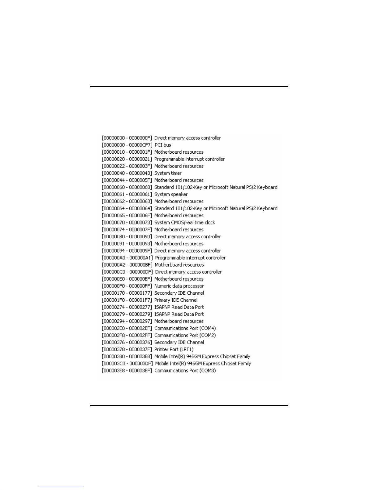
3.4 I/O Port Address Map (With CEB94000
under WinXP)
Address Devices
20
Hardware Description
Page 25

CEM830 COM Express
Address Devices
TM
Type-II Module User’s Manual
Hardware Description
21
Page 26

CEM830 COM ExpressTM Type-II Module User’s Manual
3.5 Interrupt Controller (With CEB94000
under WinXP)
IRQ Parity check error
22
Hardware Description
Page 27

CEM830 COM Express
TM
Type-II Module User’s Manual
3.6 Memory Map (With CEB94000 under
WinXP)
Address Devices
Hardware Description
23
Page 28

CEM830 COM ExpressTM Type-II Module User’s Manual
MEMO
24
Hardware Description
Page 29

CEM830 COM Express
TM
Type-II Module User’s Manual
C h a p t e r 4
Award BIOS Utility
The BIOS of CEM830 is porting with Winbond Super I/O W83627HG. If
the Baseboard designer use a different Super I/O chip, the BIOS needs
to be customized. The Phoenix-Award BIOS provides users with a
built-in Setup program to modify basic system configuration. All
configured parameters are stored in a battery-backed-up RAM (CMOS
RAM) to save the Setup information whenever the power is turned off.
4.1 Entering Setup
There are two ways to enter the Setup program. You may either turn
ON the computer and press <Del> immediately, or press the <Del>
and/or <Ctrl>, <Alt>, and <Esc> keys simultaneously when the
following message appears at the bottom of the screen during POST
(Power on Self Test).
TO ENTER SETUP PRESS DEL KEY
If the message disappears before you respond and you still want to
enter Setup, please restart the system to try it again. Turning the
system power OFF and ON, pressing the “RESET” button on the
system case or simultaneously pressing <Ctrl>, <Alt>, and <Del> keys
can restart the system. If you do not press keys at the right time and
the system doesn’t boot, an error message will pop out to prompt you
the following information:
PRESS <F1> TO CONTINUE, <CTRL-ALT-ESC> OR <DEL> TO ENTER SETUP
Award BIOS Utility
25
Page 30

CEM830 COM ExpressTM Type-II Module User’s Manual
4.2 Control Keys
Up arrow
Down arrow
Left arrow
Right arrow
Esc key
PgUp/“+” key
PgDn/“−“ key
F1 key
(Shift) F2 key
F3 key
F4 key
F5 key
F6 key
F7 key
F8 key
F9 key
F10 key
Move cursor to the previous item
Move cursor to the next item
Move cursor to the item on the left hand
Move to the item in the right hand
Main Menu -- Quit and delete changes into CMOS
Status Page Setup Menu and Option Page Setup
Menu – Exit current page and return to Main Menu
Increase the numeric value or make changes
Decrease the numeric value or make changes
General help, only for Status Page Setup Menu and
Option Page Setup Menu
Change color from total 16 colors. F2 to select color
forward, (Shift) F2 to select color backward
Reserved
Reserved
Restore the previous CMOS value from CMOS, only
for Option Page Setup Menu
Load the default CMOS value from BIOS default
table, only for Option Page Setup Menu
Load the Setup default, only for Option Page Setup
Menu
Reserved
Reserved
Save all the CMOS changes, only for Main Menu
4.3 Getting Help
z Main Menu
The online description of the highlighted setup function is displayed
at the bottom of the screen.
z Status Page Setup Menu/Option Page Setup Menu
Press <F1>
to pop out a small Help window that provides the
description of using appropriate keys and possible selections for
highlighted item
s. Press <F1> or <Esc> to exit the Help Window.
26
Award BIOS Utility
Page 31

CEM830 COM Express
TM
Type-II Module User’s Manual
4.4 The Main Menu
Once you enter the Award BIOS CMOS Setup Utility, the Main Menu
appears on the screen. In the Main Menu, there are several Setup
functions and a couple of Exit options for your selection. Use arrow
keys to select the Setup Page you intend to configure then press
<Enter> to accept or enter its sub-menu.
NOTE If your computer can not boot after making and saving
system changes with Setup, the Award BIOS will reset
your system to the CMOS default settings via its built-in
override feature.
It is strongly recommended that you should avoid changing the
chipset’s defaults. Both Award and your system manufacturer have
carefully set up these defaults that provide the best performance and
reliability.
Award BIOS Utility
27
Page 32

CEM830 COM ExpressTM Type-II Module User’s Manual
4.5 Standard CMOS Setup Menu
The Standard CMOS Setup Menu displays basic information about
your system. Use arrow keys to highlight each item, and use <PgUp>
or <PgDn> key to select the value you want in each item.
z Date
The date format is <day>, <date> <month> <year>. Press <F3> to
show the calendar.
day
date
month
year
z Time
It is determined by the BIOS and read only, from Sunday
to Saturday.
It can be keyed with the numerical/ function key, from 1
to 31.
It is from January to December.
It shows the current year of BIOS.
This item shows current time of your system with the format <hour>
<minute> <second>. The time is calculated based on the 24-hour
military-time clock. For example, 1 p.m. is 13:00:00.
28
Award BIOS Utility
Page 33

CEM830 COM Express
z IDE Primary Master/Primary Slave
TM
Type-II Module User’s Manual
These items identify the types of each IDE channel installed in the
computer. There are 45 predefined types (Type 1 to Type 45) and
2 user’s definable types (Type User) for Enhanced IDE BIOS.
Press <PgUp>/<+> or <PgDn>/<−> to select a numbered hard disk
type, or directly type the number and press <Enter>. Please be
noted your drive’s specifications must match the drive table. The
hard disk will not work properly if you enter improper information. If
your hard disk drive type does not match or is not listed, you can
use Type User to manually define your own drive type.
If selecting Type User, you will be asked to enter related
information in the following items. Directly key in the information
and press <Enter>. This information should be provided in the
documentation from your hard disk vendor or the system
manufacturer.
If the HDD interface controller supports ESDI, select “Type 1”.
If the HDD interface controller supports SCSI, select “None”.
If the HDD interface controller supports CD-ROM, select “None”.
CYLS.
HEADS
PRECOMP
number of cylinders
number of heads
write precom
LANDZONE
SECTORS
MODE
landing zone
number of sectors
HDD access mode
If there is no hard disk drive installed, select NONE and press
<Enter>.
z Dive A type/Drive B type
This item identifies the types of floppy disk drive A or drive B
installed in the computer.
None
360K, 3.5 in
1.2M, 3.5 in
720K, 3.5 in
1.44M, 3.5 in
2.88M, 3.5 in
No floppy drive installed
3.5 inch PC-type standard drive; 360Kb Mini ITXcity
3.5 inch AT-type high-density drive; 1.2MB Mini
ITXcity
3.5 inch double-sided drive; 720Kb Mini ITXcity
3.5 inch double-sided drive; 1.44MB Mini ITXcity
3.5 inch double-sided drive; 2.88MB Mini ITXcity
Award BIOS Utility
29
Page 34

CEM830 COM ExpressTM Type-II Module User’s Manual
z Halt On
This item determines whether the system will halt or not, if an error
is detected while powering up.
No errors
All errors
All, But
Keyboard
All, But
Diskette
All, But
Disk/Key
The system booting will halt on any errors detected.
(default)
Whenever BIOS detects a non-fatal error, the
system will stop and you will be prompted.
The system booting will not stop for a keyboard
error; it will stop for other errors.
The system booting will not stop for a disk error; it
will stop for other errors.
The system booting will not stop for a keyboard or
disk error; it will stop for other errors.
Press <Esc> to return to the Main Menu page.
30
Award BIOS Utility
Page 35

CEM830 COM Express
TM
Type-II Module User’s Manual
4.6 Advanced BIOS Features
This section allows you to configure and improve your system, to set
up some system features according to your preference.
Award BIOS Utility
31
Page 36

CEM830 COM ExpressTM Type-II Module User’s Manual
z CPU Feature
Scroll to this item and press <Enter> to view the CPU Feature sub
menu.
Press <Esc> to return to the Advanced BIOS Features page.
z Hard Disk Boot Priority
Scroll to this item and press <Enter> to view the sub menu to
decide the disk boot priority.
Press <Esc> to return to the Advanced BIOS Features page.
32
Award BIOS Utility
Page 37

CEM830 COM Express
z CPU L1 & L2 Cache
TM
Type-II Module User’s Manual
These two options speed up memory access. However, it depends
on the CPU/chipset design. The default setting is “Enabled”. CPUs
without built-in internal cache will not provide the “CPU Internal
Cache” item on the menu.
Enabled
Disabled
z CPU L3 Cache
Enable cache
Disable cache
Use this item to enable L3 cache only for the CPUs with such a
function.
z Hyper-Threading Technology
Use this item to enable or disable Hyper-Threading Technology,
which makes a single physical processor perform multi-tasking
function as two logical ones.
z Quick Power On Self Test
This option speeds up Power on Self Test (POST) after you turn on
the system power. If set as Enabled, BIOS will shorten or skip
some check items during POST. The default setting is “Enabled”.
Enabled
Disabled
z First/Second/Third Boot Device
These items let you select the 1
Enable Quick POST
Normal POST
st
, 2nd, and 3rd devices that the
system will search for during its boot-up sequence. The wide range
of selection includes Floppy, LS120, ZIP100, HDD0~3, SCSI, and
CDROM.
z Boot Other Device
This item allows the user to enable or disable the boot device not
listed in the First/Second/Third boot devices option above. The
default setting is “Enabled”.
z Swap Floppy Drive
This item allows you to determine whether to enable Swap Floppy
Drive or not. When enabled, the BIOS swap floppy drive
assignment makes Drive A become Drive B, and vice versa. The
default setting is “Disabled”.
Award BIOS Utility
33
Page 38

CEM830 COM ExpressTM Type-II Module User’s Manual
z Boot Up Floppy Seek
During POST, BIOS will determine the floppy disk drive type, 40 or
80 tracks. The 360Kb type is 40 tracks while 720Kb, 1.2MB and
1.44MB are all 80 tracks. The default value is “Enabled”.
BIOS searches for floppy disk drive to determine if it is
Enabled
Disabled
z Boot Up NumLock Status
40 or 80 tracks. Please be noted BIOS can not
differentiate 720K, 1.2M or 1.44M drive type as they all
are 80 tracks.
BIOS will not search for the type of floppy disk drive by
track number. There will be no warning message
displayed if the installed drive is 360K.
Set the the Num Lock status when the system is powered on.
The default value is “On”.
z Gate A20 Option
The default value is “Fast”.
Normal
Fast
The A20 signal is controlled by keyboard controller
or chipset hardware.
Default: Fast. The A20 signal is controlled by Port
92 or chipset specific method.
z Typematic Rate Setting
This item determines the typematic rate of the keyboard. The
default value is “Disabled”.
Enabled
Disabled
z Typematic Rate (Chars/Sec)
Enable typematic rate and typematic delay
programming
Disable typematic rate and typematic delay
programming. The system BIOS will use default value
of these 2 items, controlled by keyboard.
This option refers to character numbers typed per second by the
keyboard. The default value is “6”.
6
8
10
12
34
6 characters per second
8 characters per second
10 characters per second
12 characters per second
Award BIOS Utility
Page 39

CEM830 COM Express
15
20
24
30
z
Typematic Delay (Msec)
15 characters per second
20 characters per second
24 characters per second
30 characters per second
-- End of Typematic Rate Table --
This option defines how many milliseconds
TM
Type-II Module User’s Manual
must elapse before a
held-down key begins generating repeat characters. The default
value is “250”.
250
500
750
1000
z Security Option
250 msec
500 msec
750 msec
1000 msec
This item allows you to limit access to the system and Setup, or
just to Setup. The default value is “Setup”.
System
Setup
If a wrong password is entered at the prompt, the system
will not boot, the access to Setup will be denied, either.
If a wrong password is entered at the prompt, the system
will boot, but the access to Setup will be denied.
NOTE: To disable the security, select PASSWORD
SETTING at Main Menu and then you will be asked
to enter a password. Do not type anything, just
press <Enter> and it will disable the security. Once
the security is disabled, the system will boot and
you can enter Setup freely.
z APIC Mode
Use this item to enable or disable APIC (Advanced Programmable
Interrupt Controller) mode that provides symmetric multiprocessing (SMP) for systems.
z MPS Version Control For OS
This item specifies the version of the Multiprocessor Specification
(MPS). Version 1.4 has extended configuration tables to improve
support for multiple PCI bus configurations and provide future
expandability.
Award BIOS Utility
35
Page 40

CEM830 COM ExpressTM Type-II Module User’s Manual
z Small Logo<EPA> Show
Use this item to show the Logo (EPA). The default value is
“Disabled”.
z Optimized Default Select
This item allows you to select which Default Value you want to load.
The default value is “Previous Setup”.
This option allows you to load your system
BIOS Optimized
Previous Setup
configuration with default values. These default
settings are optimized to enable high performance
features.
This option allows you to load your system
configuration with Previous Setup value.
Press <Esc> to return to the Main Menu page.
4.7 Advanced Chipset Features
This section contains completely optimized chipset’s features on the
board that you are strongly recommended to leave all items on this
page at their default values unless you are very familiar with the
technical specifications of your system hardware.
36
Award BIOS Utility
Page 41

CEM830 COM Express
z DRAM Timing Selectable
TM
Type-II Module User’s Manual
Use this item to increase the timing of the memory. This is related
to the cooling of memory.
z CAS Latency Time
You can select CAS latency time to HCLKs 2, 3, or Auto. The board
designer should have set up these values in accordance with the
installed DRAM. Do not change these values unless you have to
change the specifications of the installed DRAM or CPU.
z DRAM RAS# to CAS# Delay
When DRAM is refreshed, both rows and columns are addressed
separately. This field lets you insert a timing delay between the
CAS and RAS strobe signals, used when DRAM is written to, read
from, or refreshed.
z DRAM RAS# Precharge
The precharge time is the number of cycles it takes for the RAS to
accumulate its charge before DRAM refresh. If insufficient time is
allowed, refresh may be incomplete and the DRAM may fail to
retain data.
z Precharge Delay <tRAS>
The precharge time is the number of cycles it takes for DRAM to
accumulate its charge before refresh.
z System Memory Frequency
This item helps you set main memory frequency. When using an
external graphics card, it can be adjusted to enable the best
Award BIOS Utility
37
Page 42

CEM830 COM ExpressTM Type-II Module User’s Manual
performance for your system.
z System BIOS Cacheable
Selecting Enabled allows caching of the system BIOS ROM at
F0000h-FFFFFh, resulting in better system performance. However,
if any program writes to this memory area, a system error may
result. The default value is “Disabled”.
z Video BIOS Cacheable
This item allows you to change the Video BIOS location from ROM
to RAM. Video Shadow will increase the video speed.
z PCI Express Root Port Func
Scroll to this item and press <Enter> to view the sub menu to
decide the PCI Express Port Func.
Press <Esc> to return to the Advanced Chipset Featurs page.
*** VGA Setting ***
z PEG/Onchip VGA Control
Use this item to choose the primary display card.
z On-Chip Frame Buffer Size
Use this item to set the VGA frame buffer size.
z DVMT Mode
DVMT (Dynamic Video Memory Technology) helps you select the
video mode.
38
Award BIOS Utility
Page 43

CEM830 COM Express
z DVMT/Fixed Memory Size
TM
Type-II Module User’s Manual
DVMT (Dynamic Video Memory Technology) allows you to select a
maximum size of dynamic amount usage of the video memory. The
system would configure the video memory dependent on your
application.
z Boot Display
This item is for Intel define ADD card only.
Press <Esc> to return to the Main Menu page.
Award BIOS Utility
39
Page 44

CEM830 COM ExpressTM Type-II Module User’s Manual
4.8 Integrated Peripherals
This section allows you to configure your SuperIO Device, IDE
Function and Onboard Device.
z OnChip IDE Device
Scroll to this item and press <Enter> to view the sub menu OnChip
IDE Device.
¾ IDE HDD Block Mode
Block mode is also called block transfer, multiple commands,
or multiple sector read/write. If your IDE hard drive supports
block mode (most new drives do), select Enabled for
automatic detection of the optimal number of block
read/writes per sector the drive can support.
40
Award BIOS Utility
Page 45

CEM830 COM Express
¾ IDE DMA transfer access
TM
Automatic data transfer between system memory and IDE
device with minimum CPU intervention. This improves data
throughput and frees CPU to perform other tasks.
¾ On-Chip Primary/Secondary PCI IDE
The integrated peripheral controller contains an IDE
interface with support for two IDE channels. Select Enabled
to activate each channel separately. The default value is
“Enabled”.
NOTE: Choosing Disabled for these options will
automatically remove the IDE rimaryMaster/Slave
PIO and/or IDE Secondary Master/Slave PIO items
on the menu.
¾ IDE Master/Slave PIO
The four IDE PIO (Programmed Input/Output) fields let you
set a PIO mode (0-4) for each of the four IDE devices that
the onboard IDE interface supports. Modes 0 to 4 provide
successively increased performance. In Auto mode, the
system automatically determines the best mode for each
device.
¾ IDE Master/Slave UDMA
Select the mode of operation for the IDE drive. Ultra DMA33/66/100/133 implementation is possible only if your IDE
hard drive supports it and the operating environment
includes a DMA driver. If your hard drive and system
software both support Ultra DMA-33/66/100/133, select Auto
to enable UDMA mode by BIOS.
*** On-Chip Serial ATA Setting ***
Type-II Module User’s Manual
z On-Chip Serial ATA
Use this item to enable or disable the built-in on-chip serial ATA.
z PATA IDE Mode
Use this item to set the PATA IDE mode. When set to Primary, P1
and P3 are Secondary; on the other hand, when set to Secondary,
P0 and P2 are Primary.
Press <Esc> to return to the Integrated Peripheral page.
Award BIOS Utility
41
Page 46

CEM830 COM ExpressTM Type-II Module User’s Manual
z Onboard Device
Scroll to this item and press <Enter> to view the sub menu Onboard
Device.
¾ USB Controller
Enable this item if you are using the USB in the system. You
should disable this item if a higher-level controller is added.
¾ USB 2.0 Controller
Enable this item if you are using the EHCI (USB2.0)
controller in the system.
¾ USB Keyboard Support
Enable this item if the system has a Universal Serial Bus
(USB) controller, and you have a USB keyboard.
¾ Azalia/AC’97 Audio Select
Use this item to enable or disable the onboard Azalia/AC’97
Audio function.
Press <Esc> to return to the Integrated Peripherals page.
42
Award BIOS Utility
Page 47

CEM830 COM Express
z Super IO Device
TM
Type-II Module User’s Manual
Scroll to this item and press <Enter> to view the sub menu Super
IO Device.
¾ Onboard FDC Controller
Select Enabled, if your system has a floppy disk controller
(FDC) installed on the system board and you want to use it.
If you install and-in FDC or the system has no floppy drive,
select Disabled in this field. Options: Enabled and Disabled.
¾ Onboard Serial Port 1 / 2
Select an address and corresponding interrupt for the serial
port. Options: 3F8/IRQ4, 2E8/IRQ3, 3E8/IRQ4, 2F8/IRQ3,
Disabled, Auto.
¾ URAT Mode Select
When UART Mode Select is set as ASKIR or IrDA, the
options RxD, TxD Active and IR Transmittion delay will
appear.
¾ UAR2 Duplex Mode
The second serial port offers these infrared interface modes:
1. IrDA
2. ASKIR IrDA-compliant serial infrared port
3. Normalo (default value)
NOTE The UART Mode Select will not appear on the menu
once you disable the setting of Onboard Serial Port 2.
Award BIOS Utility
43
Page 48

CEM830 COM ExpressTM Type-II Module User’s Manual
¾ Onboard Paralellel Port 3/4
This item allows you to determine the I/O address for
onboard parallel port.
¾ Onboard Parallel Port
This item is used to assign the I/O address and interrupt
request (IRQ) for the onboard parallel port.
¾ Parallel Port Mode
Select an operating mode for the onboard parallel (printer)
port. Select Normal unless your hardware and software
require another mode in this field. Options: EPP1.9, ECP,
SPP, ECPEPP1.7, EPP1.7.
¾ EPP Mode Select
Select EPP port type 1.7 or 1.9.
¾ ECP Mode Use DMA
Select a DMA channel for the parallel port while using the
ECP mode.
Press <Esc> to return to the Integrated Peripherals page, and press it
again to the Main Menu page.
4.9 Power Management Setup
The Power Management Setup allows you to save energy of your
system effectively. It will shut down the hard disk and turn OFF video
display after a period of inactivity.
44
Award BIOS Utility
Page 49

CEM830 COM Express
z ACPI Function
TM
Type-II Module User’s Manual
This item allows you to enable/disable the Advanced Configuration
and Power Management (ACPI). The function is always “Enabled”.
z ACPI Suspend Type
This item specifies the power saving modes for ACPI function. If
your operating system supports ACPI, such as Windows 98SE,
Windows ME and Windows 2000, you can choose to enter the
Standby mode in S1 (POS) or S3 (STR) fashion through the setting
of this field. Options are:
[S1 (POS)] The S1 sleep mode is a low power state. In this
state, no system context is lost (CPU or chipset) and
hardware maintains all system contexts.
[S3 (STR)] The S3 sleep mode is a lower power state where
the information of system configuration and open
applications/files is saved to main memory that remains
powered while most other hardware components turn off to
save energy. The information stored in memory will be used
to restore the system when a “wake up” event occurs.
z Power Management
This option allows you to select the type of power Management.
Options: APM, ACPI.
Award BIOS Utility
45
Page 50

CEM830 COM ExpressTM Type-II Module User’s Manual
z Video Off Method
This setting determines the manner in which the monitor is blanked.
V/H
SYNC+Blank
DPMS
Blank Screen
z Video Off In Suspend
It turns OFF vertical and horizontal synchronization ports
and writes blanks to the video buffer.
Select this option if your monitor supports the Display
Power Management Signaling (DPMS) standard of the
Video Electronics Standards Association (VESA). Use
the supplied software for your video subsystem to select
video power management values.
The System only writes blanks to the video buffer.
This item defines if the video is powered down when the system is
put into suspend mode.
z Suspend Type
If this item is set to the default Stop Grant, the CPU will go into Idle
Mode during power saving mode.
z Moden Use IRQ
If you want an incoming call on a modem to automatically resume
the system from a powersaving mode, use this item to specify the
interrupt request line (IRQ) used by the modem. You might have to
connect the fax/modem to the board Wake On Modem connector
for working this feature.
1. Suspend Mode
After a selected period of system inactivity (1 minute to 1 hour), all
devices except the CPU shut off. The default value is “Disabled”.
Disabled
1/2/4/6/8/10/
20/30/40
Min/1 Hr
2. HDD Power Down
If HDD activity is not detected for a specified length of time in this field,
the hard disk drive will be powered down while other devices remain
active
.
The System will never enter the SUSPEND mode.
It defines continuous idle time before the system
entering the SUSPEND mode.
If any item defined in (J) is enabled and active, the
SUSPEND timer will be reloaded.
46
Award BIOS Utility
Page 51

CEM830 COM Express
z Soft-Off by PWR-BTTN
TM
Type-II Module User’s Manual
This option only works with systems using an ATX power supply. It
also allows users to define which type of soft power OFF sequence
the system will follow. The default value is “Instant-Off”.
This option follows the conventional manner of system
Instant-Off
Delay 4 Sec.
z Wake-Up by PCI card
performance when turning the power to OFF. InstantOff is a software power OFF sequence requiring the
power supply button is switched to OFF.
Upon the system’s turning OFF through the power
switch, this option will delay the complete system power
OFF sequence approximately 4 seconds. Within this
delay period, the system will temporarily enter into the
Suspend Mode enabling you to restart the system at
once.
If enable this item, the system can automatically resume when the
PCI Modem or PCI LAN card receives an incoming call.
z Power On by Ring
This option allows the system to resume or wake up upon detecting
any ring signals coming from an installed modem. The default value
is “Enabled”.
z Resume by Alarm
If enable this item, the system can automatically resume after a
fixed time in accordance with the system’s RTC (realtime clock).
Press <Esc> to return to the Main Menu page.
Award BIOS Utility
47
Page 52

CEM830 COM ExpressTM Type-II Module User’s Manual
4.10 PnP/PCI Configuration Setup
This section describes the configuration of PCI (Personal Computer
Interconnect) bus system, which allows I/O devices to operate at
speeds close to the CPU speed while communicating with other
important components. This section covers very technical items that
only experienced users could change default settings.
z Init Display First
This item allows you to decide whether PCI Slot or AGP to be the
first primary display card.
z Reset Configuration Data
Normally, you leave this item Disabled. Select Enabled to reset
Extended System Configuration Data (ESCD) when you exit Setup
or if installing a new add-on cause the system reconfiguration a
serious conflict that the operating system can not boot. Options:
Enabled, Disabled.
z Resources Controlled By
The Award Plug and Play BIOS can automatically configure all
boot and Plug and Play-compatible devices. If you select Auto, all
interrupt request (IRQ), DMA assignment, and Used DMA fields
disappear, as the BIOS automatically assigns them. The default
value is “Manual”.
48
Award BIOS Utility
Page 53

CEM830 COM Express
z IRQ Resources
TM
Type-II Module User’s Manual
When resources are controlled manually, assign each system
interrupt to one of the following types in accordance with the type
of devices using the interrupt:
1. Legacy ISA Devices compliant with the original PC AT bus
specification, requiring a specific interrupt (such as IRQ4 for serial port
1).
2. PCI/ISA PnP Devices compliant with the Plug and Play standard,
whether designed for PCI or ISA bus architecture.
The default value is “PCI/ISA PnP”
z PCI/VGA Palette Snoop
.
Some non-standard VGA display cards may not show colors
properly. This item allows you to set whether MPEG ISA/VESA
VGA Cards can work with PCI/VGA or not. When enabled, a
PCI/VGA can work with a MPEG ISA/VESA VGA card; when
disabled, a PCI/VGA cannot work with a MPEG ISA/VESA Card.
Press <Esc> to return to the Main Menu page.
Award BIOS Utility
49
Page 54

CEM830 COM ExpressTM Type-II Module User’s Manual
4.11 PC Health Status
This section supports hardware monitering that lets you monitor those
parameters for critical voltages, temperatures and fan speed of the
board.
z System Component Characteristics
These read-only items show you information about the system’s
current operating status, and the functions of the hardware thermal
sensor monitoring the chipset blocks and system temperatures to
ensure a stable system.
1. System Temperature
2. Expanded Temperature
3. CPU Temperature
4. Current FAN1/2 Speed
5. CPU Voltage
Press <Esc> to return to the Main Menu page.
50
Award BIOS Utility
Page 55

CEM830 COM Express
TM
Type-II Module User’s Manual
4.12 Frequency/Voltage Control
This section is to control the CPU frequency and Supply Voltage,
DIMM OverVoltage and AGP voltage.
z Auto Detect PCI Clk
The enabled item can automatically disable the clock source for a
PCI slot without a module, to reduce EMI (ElectroMagnetic
Interference).
z Spread Spectrum
If spread spectrum is enabled, EMI (ElectroMagnetic Interference)
generated by the system can be significantly reduced.
Press <Esc> to return to the Main Menu page.
Award BIOS Utility
51
Page 56

CEM830 COM ExpressTM Type-II Module User’s Manual
4.13 Load Optimized Defaults
This option allows you to load your system configuration with default
values. These default settings are optimized to enable high
performance features.
To load CMOS SRAM with SETUP default values, please enter “Y”. If
not, please enter “N”.
52
Award BIOS Utility
Page 57

CEM830 COM Express
TM
Type-II Module User’s Manual
4.14 Set Supervisor/User Password
You can set either supervisor or user password, or both of then. The
differences between are:
1. Supervisor password: can enter and change the options of the
setup menus.
2. User password: just can enter but do not have the right to change
the options of the setup menus.
When you select this function, the following message will appear at the
center of the screen to assist you in creating a password.
ENTER PASSWORD:
Type the password with eight characters at most, and press <Enter>.
The password typed will now clear any previously entered password
from CMOS memory. You will be asked to confirm the password. Type
the password again and press <Enter>. You may also press <Esc> to
abort the selection and not enter a password.
To disable password, just press <Enter> when you are prompted to
enter password. A message will confirm the password being disabled.
Once the password is disabled, the system will boot and you can enter
Setup freely.
PASSWORD DISABLED.
When a password is enabled, you have to type it every time you enter
Setup. This prevents any unauthorized person from changing your
system configuration.
Additionally when a password is enabled, you can also require the
BIOS to request a password every time the system reboots. This would
prevent unauthorized use of your computer.
You determine when the password is required within the BIOS
Features Setup Menu and its Security option. If the Security option is
set to “System”, the password is required during boot up and entry into
Setup. If set as “Setup”, prompting will only occur prior to entering
Setup.
Award BIOS Utility
53
Page 58

CEM830 COM ExpressTM Type-II Module User’s Manual
4.15 Save & Exit Setup
This allows you to determine whether or not to accept the modifications.
Typing “Y” quits the setup utility and saves all changes into the CMOS
memory. Typing “N” brigs you back to Setup utility.
54
Award BIOS Utility
Page 59

CEM830 COM Express
TM
Type-II Module User’s Manual
4.16 Exit Without Saving
Select this option to exit the Setup utility without saving the changes
you have made in this session. Typing “Y” will quit the Setup utility
without saving the modifications. Typing “N” will return you to Setup
utility.
Award BIOS Utility
55
Page 60

CEM830 COM ExpressTM Type-II Module User’s Manual
MEMO
56
Award BIOS Utility
Page 61

CEM830 COM ExpressTM Type II Module User’s Manual
A p p e n d i x A
Watchdog Timer
Watchdog Timer Setting
(From CEB94000 Super I/O W83627HG)
After the system stops working for a while, it can be auto-reset by the
Watchdog Timer. The integrated Watchdog Timer can be set up in the
system reset mode by program.
Using the Watchdog Function
Start
↓
Un-Lock WDT:
O 2E 87 ; Un-lock super I/O
O 2E 87 ; Un-lock super I/O
↓
Select Logic device:
O 2E 07
O 2F 08
↓
Activate WDT:
O 2E 30
O 2F 01
↓
Set Second or Minute :
O 2E F5
O 2F N N=00 or 08(See below table)
↓
Set base timer :
O 2E F6
O 2F M=00,01,02,…FF(Hex) ,Value=0 to 255
↓
WDT counting re-set timer :
O 2E F6
O 2F M ; M=00,01,02,…FF(See below table)
Watchdog Timer
57
Page 62

CEM830 COM ExpressTM Type-II Module User’s Manual
; IF to disable WDT:
O 2E 30
O 2F 00 ; Can be disable at any time
z Timeout Value Range
1 to 255
Minute / Second
z Program Sample
Watchdog Timer can be set to system reset after 5-second timeout.
2E, 87
2E, 87
2E, 07
2F, 08
2E, 30
2F, 01
2E, F5
2F, N
2E, F6
2F, M
Logical Device 8
Activate
Set Minute or Second
N=08 (Min),00(Sec)
Set Value
M = 00 ~ FF
58
Watchdog Timer
Page 63

CEM830 COM ExpressTM Type II Module User’s Manual
A p p e n d i x B
GPIO & Watchdog Timer
Programming Source Code
(From CEM830 Fintek F75111R)
Programming Source Code
/*---------------- INCLUDE FILE ---------------------*/
#include <stdio.h>
#include <conio.h>
#include <bios.h>
#define UCHAR unsigned char
#define UINT unsigned int
#define SMIOBASE 0x5000
/*****************
SMIOBASE can get from PCI device Bus-0,Device31,Function-3
Register 20h~23h, the value is the IO base address.
******************/
#define SM_REG (SMIOBASE+3)
#define SM_ADDR (SMIOBASE+4)
#define SM_DATA (SMIOBASE+5)
#define SM_CMD (SMIOBASE+2)
#define SM_STATUS (SMIOBASE+0)
#define SM_byteAccess 0x48
#define Device_Addr 0x6E //depend on hardwire designed
UCHAR _read_smbus(UCHAR ,UCHAR);
void _write_smbus(UCHAR,UCHAR, UCHAR);
#define F75111_CHIPID 0x0003
#define F75111_VENDORID 0x3419
#define WDTOUT10_CntlReg1 0x34
#define WDTOUT10_2S_bit 0x04 //bit 2
#define WDTOUT10_OINV_bit 0x02 //bit 1
#define WDTOUT10_Status_bit 0x01 //bit 0 , write 1 for clear
status
#define WDTOUT10_CntlReg2 0x35
#define WDTOUT10_Enable_bit 0x80 //bit 7
#define WDTOUT10_PTIME 0x7f //bit 0~6
GPIO & Watchdog Timer Programming Source Code
59
Page 64

CEM830 COM ExpressTM Type-II Module User’s Manual
/* ------------------ MAIN PROGRAM ------------------*/
main()
{
UCHAR xch,xch2;
UINT chipid=0, vendorid=0;
//Check the Chip ID information
xch=_read_smbus(Device_Addr,0x5a); //Chip ID 1
xch2=_read_smbus(Device_Addr,0x5b); //Chip ID 2
chipid=((UINT)xch2 << 8) + (UINT)xch;
xch=_read_smbus(Device_Addr,0x5d); //Vendor ID 1
xch2=_read_smbus(Device_Addr,0x5E); //Vendor ID 2
vendorid=((UINT)xch2 << 8) + (UINT)xch;
if (F75111_CHIPID != chipid || F75111_VENDORID != vendorid )
{ printf("!!! Not found F75111 chip !!!\n" );
exit(-1);
}
printf("=== Found F75111 chip ===\n");
printf("=== GPIO Output Test ===\n");
//set GPIO3x direction
printf("Set F75111 GPIO3x pin is output direction\n");
_write_smbus(Device_Addr,0x40,0x0f); //GPIO3x Output
direction
//set GPIO3x output level or plus
printf("Set F75111 GPIO3x pin is output Level\n");
_write_smbus(Device_Addr,0x43,0); //GPIO3x Level control
//write GPIO3x data
printf("Write GPIO3x data is 0x0A\n");
printf("GPO0=0, GPO1=1, GPO2=0, GPO3=1\n");
_write_smbus(Device_Addr,0x41,0x0a);
printf("Please check the GPO level and hit any key to
continue\n");
getch();
//write GPIO3x data
printf("Write GPIO3x data is 0x05\n");
printf("GPO0=1, GPO1=0, GPO2=1, GPO3=0\n");
_write_smbus(Device_Addr,0x41,0x05);
printf("Please check the GPO level and hit any key to
continue\n");
getch();
60
GPIO & Watchdog Timer Programming Source Code
Page 65

CEM830 COM ExpressTM Type II Module User’s Manual
//set GPIO10,11,12 used
printf("=== GPIO Input Test ===\n");
printf("Set F75111 GPIO1x is used GPIO function\n");
xch=_read_smbus(Device_Addr,0x03);
xch &= 0xE0 ;
_write_smbus(Device_Addr,0x03,xch); //set Pin GPIO10/11/12
used
_write_smbus(Device_Addr,0x04,0); //set Pin GPIO1x used
printf("Set F75111 GPIO10,11,12,13 is input function\n");
_write_smbus(Device_Addr,0x10,0x00); //set GPIO1x input
direction
printf("Set F75111 GPIO10,11,12,13 is Level mode\n");
_write_smbus(Device_Addr,0x13,0x00); //set GPIO1x Level
Control
xch=_read_smbus(Device_Addr,0x12); //read GPIO1x Status
printf("Read the GPI0,1,2,3 input data is %02X\n",xch);
printf("Please Change the GPIx input and hit any key to
continue\n");
getch();
xch=_read_smbus(Device_Addr,0x12); //read GPIO1x Status
printf("Read the GPI0,1,2,3 input data is %02X\n",xch);
printf("Please Change the GPIx input and hit any key to
continue\n");
getch();
xch=_read_smbus(Device_Addr,0x12); //read GPIO1x Status
printf("Read the GPI0,1,2,3 input data is %02X\n",xch);
/*********************************************/
printf("===== WatchDogTimer Test =====\n");
printf("Set WDTOUT10 pin used\n");
_write_smbus(Device_Addr,0x01,0x20); //Pin1 config
printf("Set WDTOUT10 output 100ms plus, normal level\n");
_write_smbus(Device_Addr,WDTOUT10_CntlReg1,0);
//WDT10 control
printf("Set WDTOUT10 Time 10 seconds and enable WDT\n");
_write_smbus(Device_Addr,WDTOUT10_CntlReg2,0x8A);
//WDT10 control
printf("Please hit any key in period of 10 seconds\n");
getch();
_write_smbus(Device_Addr,WDTOUT10_CntlReg2,0x8A);
//WDT10 control
printf("The sytsem will reset when the 10 seconds times
GPIO & Watchdog Timer Programming Source Code
61
Page 66

CEM830 COM ExpressTM Type-II Module User’s Manual
out\n");
}
void _write_smbus(UCHAR xAddr,UCHAR xReg, UCHAR xData)
{
while (1)
{ if (_check_smbus_busy()==0) break;
}
outp(SM_REG, xReg);
xdelay(); //because the CPU too fast,delay for IO
outp(SM_ADDR, xAddr);
xdelay(); //because the CPU too fast,delay for IO
outp(SM_DATA, xData);
xdelay(); //because the CPU too fast,delay for IO
outp(SM_CMD, SM_byteAccess);
xdelay(); //because the CPU too fast,delay for IO
outp(SM_STATUS, 02); //clear interrupt status
}
UCHAR _read_smbus(UCHAR xAddr,UCHAR xReg)
{
UCHAR xch,xch2;
while (1)
{ if (_check_smbus_busy()==0) break;
}
outp(SM_REG, xReg);
xdelay(); //because the CPU too fast,delay for IO
outp(SM_ADDR, xAddr+1);
xdelay(); //because the CPU too fast,delay for IO
outp(SM_CMD, SM_byteAccess);
xdelay(); //because the CPU too fast,delay for IO
while (1)
{ if (_check_smbus_busy()==0) break;
}
xch=inp(SM_DATA);
xdelay(); //because the CPU too fast,delay for IO
outp(SM_STATUS, 2); //clear interrupt status
return xch;
}
_check_smbus_busy(void)
{
UCHAR xch;
xch=inp(SM_STATUS);
if (xch & 0x02 ) outp(SM_STATUS, 2); //clear interrupt
status
if ( xch & 0x02 ) return 1;
if ( xch & 0x01 ) return 1;
return 0;
62
GPIO & Watchdog Timer Programming Source Code
Page 67

CEM830 COM ExpressTM Type II Module User’s Manual
}
xdelay()
{
int xxi,xxj,xxk=0;
for (xxi=0 ; xxi< 0x1000 ; xxi++) {
for (xxj=0 ; xxj < 0x100 ; xxj++) {
xxk++;
}
}
}
GPIO & Watchdog Timer Programming Source Code
63
Page 68

CEM830 COM ExpressTM Type-II Module User’s Manual
MEMO
64
GPIO & Watchdog Timer Programming Source Code
Page 69

CEM830 COM ExpressTM Type II Module User’s Manual
A p p e n d i x C
Configuring SATA for RAID Function
Configuring SATA Hard Drive(s) for RAID
®
Function (Controller: Intel
Please follow up the steps below to configure SATA hard drive(s):
(1) Install SATA hard drive(s) in your system.
(2) Enter the BIOS Setup to configure SATA controller mode and boot
sequence.
(3) Configure RAID by the RAID BIOS.
(4) Create a floppy disk for the SATA controller driver.
(5) Install the SATA controller driver during the OS installation.
Before you begin the SATA configuration, please prepare:
(a) Two SATA hard drives (to ensure optimal performance, it is
recommended that you use two hard drives with identical model
and capacity).
(b) An empty formatted floppy disk
(c) Windows XP setup disk
(1) Installing SATA hard drive(s) in your system
Connect one end of the SATA signal cable to the rear of the SATA
hard drive, and the other end to available SATA port(s) on the
board. Then, connect the power connector of power supply to the
hard drive.
(2) Configuring SATA controller mode and boot sequence by the
BIOS Setup
You have to make sure whether the SATA controller is configured
correctly by system BIOS Setup and set up BIOS boot sequence for
the SATA hard drive(s).
ICH7-M DH only)
Configuring SATA for RAID Function
65
Page 70

CEM830 COM ExpressTM Type-II Module User’s Manual
(2)-1 Turn on your system and press the Del button to enter BIOS
Setup during running POST (Power-On Self Test). If you want
to create RAID, just select RAID for SATA Mode (default IDE)
under the Integrated Peripherals menu.
Figure 1
66
Configuring SATA for RAID Function
Page 71

CEM830 COM ExpressTM Type II Module User’s Manual
(2)-2 Set CDROM for First Boot Device under the Advanced
BIOS Features menu to boot CD-ROM after system restarts
(Figure 2).
Figure 2
(2)-3 Save and exit the BIOS Setup.
(3) Configuring RAID by the RAID BIOS
Enter the RAID BIOS setup utility to configure a RAID array.
Configuring SATA for RAID Function
67
Page 72

CEM830 COM ExpressTM Type-II Module User’s Manual
(3)-1 After the POST memory testing and before the operating
system booting, a message "Press <Ctrl-I> to enter
Configuration Utility" (as Figure 3) shows up, accordingly,
press <CTRL+ I> to enter the RAID BIOS setup utility.
Figure 3
(3)-2 After you press <CTRL+ I>, the Create RAID Volume screen
will appear (as Figure 4). If you want to create a RAID array,
select the Create RAID Volume option in the Main Menu and
press ENTER.
Figure 4
68
Configuring SATA for RAID Function
Page 73

CEM830 COM ExpressTM Type II Module User’s Manual
(3)-3 After entering the CREAT VOLUME MENU screen, you can
type the disk array name with 1~16 letters (letters cannot be
special characters) in the item “Name”. When finished, press
ENTER to select a RAID level (as Figure 5). There are two
RAID levels, RAID0 and RAID1. Select a RAID level and
press ENTER.
Figure 5
(3)-4 Set the stripe block size (as Figure 6). The KB is the standard
unit of stripe block size. The stripe block size can be 4KB to
128KB. After the setting, press ENTER for the array capacity.
Figure 6
Configuring SATA for RAID Function
69
Page 74

CEM830 COM ExpressTM Type-II Module User’s Manual
(3)-5 After setting all the items on the menu, select Create Volume
and press ENTER (as Figure 7) to start creating the RAID
array.
Figure 7
(3)-6 When prompting the confirmation, press “Y“ to create this
volume, or “N“ to cancel the creation.
Figure 8
70
Configuring SATA for RAID Function
Page 75

CEM830 COM ExpressTM Type II Module User’s Manual
After the creation is completed, you can see detailed information about
the RAID Array in the DISK/VOLUME INFORMATION section,
including RAID mode, disk block size, disk name, disk capacity, etc.
Figure 9
Delete RAID Volume
If you want to delete a RAID volume, select the Delete RAID Volume
option in Main Menu. Press ENTER and follow on-screen instructions.
Figure 10
Configuring SATA for RAID Function
71
Page 76

CEM830 COM ExpressTM Type-II Module User’s Manual
Please press [ESC] to exit the ICH7MR RAID BIOS utility.
Now, you can proceed to install a SATA controller and the operating
system.
(4) Making a SATA Driver Disk
To install the operating system onto a serial ATA hard disk successfully,
you need to install the SATA controller driver during the OS installation.
Without the driver, the hard disk may not be recognized during the
Windows setup process. First of all, please format a blank floppy disk.
Secondly, follow up these steps below to produce a SATA driver disk.
(4)-1 Users can insert the Driver CD and the formatted blank floppy
disk in another system. And then, please execute the
f6flpy32.exe file in the folder of the Driver CD.
Note Please execute the f6flpy64.exe file, if installing 64-
bit Windows Operating System.
(4)-2 When this screen pops out, please click the “CONFIRM” button.
72
Configuring SATA for RAID Function
Page 77

CEM830 COM ExpressTM Type II Module User’s Manual
(4)-3 When the Driver is written to the floppy disk, the SATA driver
disk is completed.
(5) Installing the SATA controller driver during the OS installation
Now, the SATA driver disk is ready, and BIOS settings configured, you
can proceed to install Windows XP onto your SATA hard drive using
the SATA driver. Here is an example for Windows XP installation.
Configuring SATA for RAID Function
73
Page 78

CEM830 COM ExpressTM Type-II Module User’s Manual
(5)-1 Restart your system to boot the Windows XP Setup disk, and
press F6 button as soon as you see the message "Press F6 if
you need to install a 3rd party SCSI or RAID driver" (as
Figure 11). After pressing the F6 button, there will be a few
moments for some files being loaded before next screen
appears.
Figure 11
(5)-2 When you see the screen below, insert the floppy disk
containing the SATA driver and press “S” (as Figure 12).
Figure 12
74
Configuring SATA for RAID Function
Page 79

CEM830 COM ExpressTM Type II Module User’s Manual
(5)-3 If the Setup correctly recognizes the driver of the floppy disk,
a controller menu (as Figure 13) will appear below. Use the
ARROW keys to select Intel(R) 82801 GHM SATA RAID
Controller (Mobile ICH7MDH) and press ENTER. Then it will
begin to load the SATA driver from the floppy disk.
Figure 13
Note
If a message on the screen saying that one or some
file(s) cannot be found, please check the floppy disk or
copy the correct SATA driver again from the driver CD.
Configuring SATA for RAID Function
75
Page 80

CEM830 COM ExpressTM Type-II Module User’s Manual
(5)-4 When the screen appears as below, press ENTER to
continue installing the SATA driver through the floppy disk. It
will take about one minute to finish the driver installation.
Figure 14
After the SATA controller driver installation is completed, you can
proceed to install the Windows XP.
76
Configuring SATA for RAID Function
 Loading...