

Page 1

CEB94011
COM Express
TM
Type 6
Development Baseboard
User’s Manual
Page 2

ii
Disclaimers
This manual has been carefully checked and believed to contain accurate information.
Axiomtek Co., Ltd. assumes no responsibility for any infringements of patents or any third
party’s rights, and any liability arising from such use.
Axiomtek does not warrant or assume any legal liability or responsibility for the accuracy,
completeness or usefulness of any information in this document. Axiomtek does not make any
commitment to update the information in this manual.
Axiomtek reserves the right to change or revise this document and/or product at any time
without notice.
No part of this document may be reproduced, stored in a retrieval system, or transmitted, in
any form or by any means, electronic, mechanical, photocopying, recording, or otherwise,
without the prior written permission of Axiomtek Co., Ltd.
CAUTION
If you replace wrong batteries, it causes the danger of explosion. It is recommended by the
manufacturer that you follow the manufacturer’s instructions to only replace the same or
equivalent type of battery, and dispose of used ones.
Copyright 2017 Axiomtek Co., Ltd.
All Rights Reserved
March 2017, Version A1
Printed in Taiwan
Page 3

iii
ESD Precautions
Computer boards have integrated circuits sensitive to static electricity. To prevent chipsets
from electrostatic discharge damage, please take care of the following jobs with precautions:
Do not remove boards or integrated circuits from their anti-static packaging until you are
ready to install them.
Before holding the board or integrated circuit, touch an unpainted portion of the system
unit chassis for a few seconds. It discharges static electricity from your body.
Wear a wrist-grounding strap, available from most electronic component stores, when
handling boards and components.
Trademarks Acknowledgments
Axiomtek is a trademark of Axiomtek Co., Ltd.
Intel
®
and Celeron® are trademarks of Intel Corporation.
Windows
®
is a trademark of Microsoft Corporation.
AMI is trademark of American Megatrend Inc.
IBM, PC/AT, PS/2, VGA are trademarks of International Business Machines Corporation.
Other brand names and trademarks are the properties and registered brands of their
respective owners.
Page 4

iv
Table of Contents
Disclaimers ..................................................................................................... ii
ESD Precautions ........................................................................................... iii
Chapter 1 Introduction ............................................. 1
1.1 Features ............................................................................................... 1
1.2 Specifications ...................................................................................... 2
1.3 Utilities Supported .............................................................................. 3
Chapter 2 Board and Pin Assignments .................... 5
2.1 Board Dimensions and Fixing Holes ................................................. 5
2.2 Board Layout ....................................................................................... 7
2.3 Installing CEM Module and Heatsink ................................................. 8
2.4 Jumper Settings ................................................................................ 10
2.4.1 Auto Power On (JP1) ................................................................................. 11
2.4.2 LVDS Voltage Selection (JP5) .................................................................... 11
2.4.3 LV DS/eDP Function Selection (JP6) .......................................................... 11
2.4.4 Boot BIOS Selection (JP7) ......................................................................... 11
2.4.5 Power Input Mode Selection (JP9 and JP11) ............................................ 11
2.4.6 Restore BIOS Optimal Defaults (JP10) ..................................................... 12
2.4.7 DIO/SD Card Function Selection (JP12) ................................................... 12
2.4.8 Thermal Trip Indicator (JP13) .................................................................... 12
2.4.9 LV DS Brightness Control Mode Setting (JP14) ........................................ 12
2.5 Connectors ........................................................................................ 13
2.5.1 DVI-D Connector (CN1) ............................................................................ 14
2.5.2 HDMI Connector (CN2) ............................................................................. 14
2.5.3 Front Panel Connector (CN3) ................................................................... 15
2.5.4 DisplayPort Connector (CN4) .................................................................... 16
2.5.5 Audio Jack (CN5) ...................................................................................... 16
2.5.6 Ethernet and USB 2.0 Port Stack (CN6) ................................................... 17
2.5.7 USB 3.0 Stacks (CN7 and CN8) ............................................................... 18
2.5.8 ATX Power Connectors (CN9 and CN27) ................................................. 19
2.5.9 COM D-Sub Connector (CN10) ................................................................ 20
2.5.10 PCI-Express Mini Card Connectors (CN11 and CN13) ............................ 20
2.5.11 VGA Connector (CN12) ............................................................................. 21
2.5.12 I2C Connectors (CN14 and CN26) ........................................................... 21
2.5.13 Inverter Connector (CN15) ........................................................................ 21
2.5.14 SA TA Power Connectors (CN16 and CN17) ............................................. 22
2.5.15 Wide Range Power Input Connectors (CN18) .......................................... 22
2.5.16 SD Card Slot (CN19) ................................................................................. 22
Page 5

v
2.5.17
COM1 and COM2 Connectors (CN20 and CN21) .................................... 23
2.5.18 Digital I/O Port Connector (CN22) ............................................................. 23
2.5.19 SMBus Connector (CN23) ........................................................................ 24
2.5.20 eDP Connector (eDP1) ............................................................................. 25
2.5.21 LVDS Connector (LVDS1) ......................................................................... 26
2.5.22 CPU Fan Connector (FAN1) ..................................................................... 28
2.5.23 SA TA Connectors (SATA1~SATA4) ........................................................... 28
2.5.24 COM ExpressTM Connectors (RECS1 and RECS2) ................................. 28
2.6 Push Buttons ..................................................................................... 31
2.7 LED Indicators ................................................................................... 31
Page 6

vi
This page is intentionally left blank.
Page 7
CEB94011 COM ExpressTM Type 6 Development Baseboard
Introduction 1
Chapter 1
Introduction
The CEB94011 is a new COM ExpressTM type 6 development baseboard equipped with an
embedded COM Express
TM
CPU type 6 module and fully compliant with the PCI Industrial
Computer Manufactures PICMG COM Express
TM
standard. The COM ExpressTM is an open
industry standard for Computer-on-Modules, designed to be future proof and to provide a
smooth transition path from legacy parallel interfaces to LVDS/eDP interfaces. In addition to
the standard output signals for converting, CEB94011 provides one PCI Express x16 slot for
graphics, one PCI Express x4 slot, two PCI Express x1 slots and two PCI-Express Mini Card
sockets for expansion purposes.
This board supports various I/O features: display interfaces (VGA, LVDS/eDP, DisplayPort,
HDMI and DVI-D), Gigabit/Fast Ethernet, HD audio codec, four SATA-600 interfaces, six USB
ports (2 USB 2.0 and 4 USB 3.0 ports), digital I/O or SD card slot, two RS-232 ports and two
RS-232/422/485 ports.
With CEB94011, customers can develop their own applications and upgrade the system
configuration in advance to meet faster time-to-market.
1.1 Features
COM Express
TM
type 6 baseboard for evaluation purpose
USB 3.0 supported
Port 80 display for debugging
Switch button for PWRBTN, RESET, SLEEP, LID
Page 8

CEB94011 COM ExpressTM Type 6 Development Baseboard
2 Introduction
1.2 Specifications
CPU
COM Express
TM
type 6 module.
System Chipset
On the COM Express
TM
module.
BIOS
On the COM Express
TM
module.
System Memory
On the COM Express
TM
module.
Onboard Multi I/O
Two RS-232 TX/RX ports.
Two RS-232/422/485 ports.
Serial ATA
Four SATA-600 connectors.
Ethernet
One RJ-45 interface for 1000/100/10Mbps.
Audio
HD audio with line-in/line-out and MIC-in audio jack.
USB Interface
Two USB ports with fuse protection and comply with USB Spec. Rev. 2.0.
Four USB ports comply with USB Spec. Rev. 3.0.
SPI
Supported.
SMBus
Supported.
SD card slot
One SD card slot
Digital I/O
Four input channels and four output channels.
Port 80 Display
Dual 7 segments Port 80 display for convenient debugging purpose through LPC
interface.
Display
One 40-pin connector for 18/24-bit single/dual channel LVDS and one 8-pin inverter
connector.
One eDP connector.
One 15-pin D-Sub connector as VGA connector.
One Display Port.
One HDMI.
One DVI-D.
Page 9

CEB94011 COM ExpressTM Type 6 Development Baseboard
Introduction 3
Expansion Interface
One PCIe x16 slot.
One PCIe x4 slot.
Two PCI-Express Mini Card socket which complies with PCI-Express Mini Card
Spec. V1.2.
Two PCIe x1 slots.
Battery
Lithium 3V/220mAH.
Size
244 x 291mm.
Board Thickness
1.6mm.
Operation Temperature
-40°C ~ +85°C (-104°F ~ 185°F).
Operation Humidity
10% ~ 95% relative humidity, non-condensing.
Note
All specifications and images are subject to change without notice.
1.3 Utilities Supported
Audio driver
Page 10

CEB94011 COM ExpressTM Type 6 Development Baseboard
4 Introduction
This page is intentionally left blank.
Page 11
CEB94011 COM ExpressTM Type 6 Development Baseboard
Board and Pin Assignments 5
Chapter 2
Board and Pin Assignments
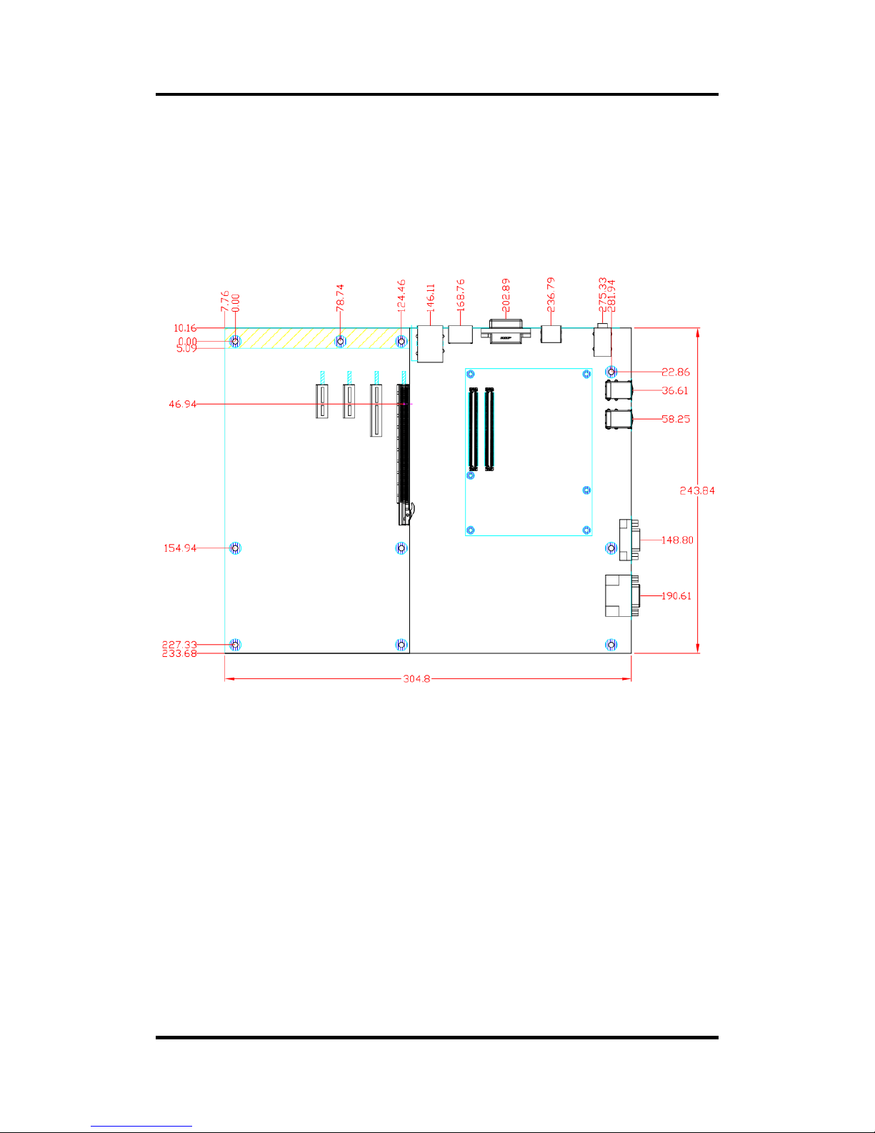
2.1 Board Dimensions and Fixing Holes
T op Side
Page 12
CEB94011 COM ExpressTM Type 6 Development Baseboard
6 Board and Pin Assignments
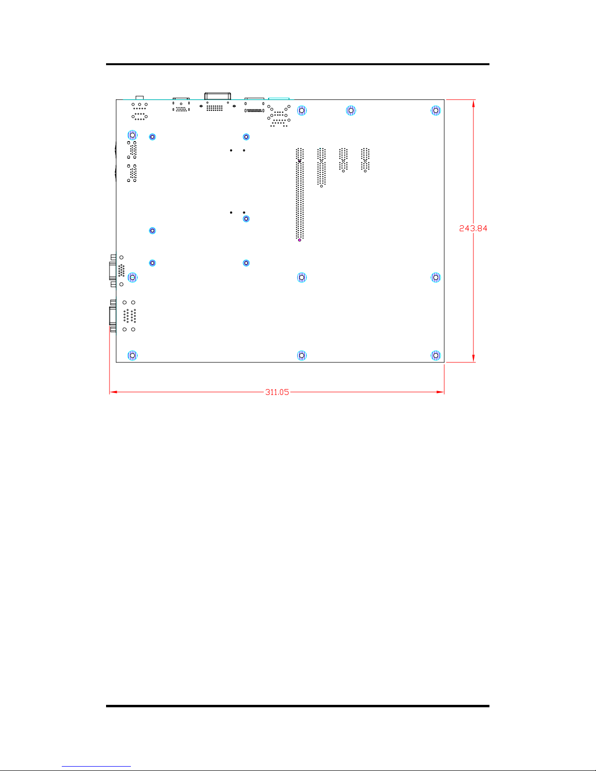
Bottom Side
Page 13

CEB94011 COM ExpressTM Type 6 Development Baseboard
Board and Pin Assignments 7
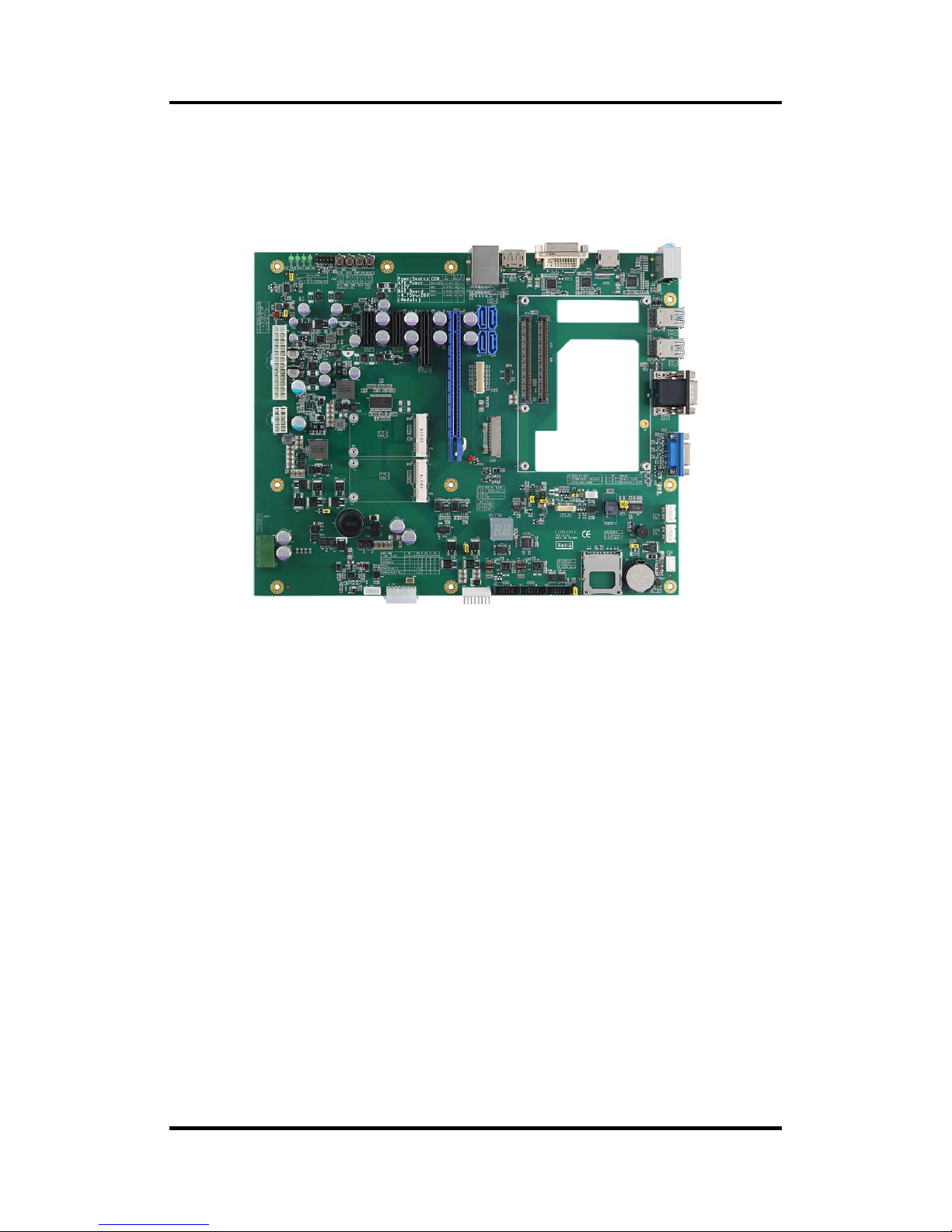
2.2 Board Layout
T op Side
Page 14

CEB94011 COM ExpressTM Type 6 Development Baseboard
8 Board and Pin Assignments
2.3 Installing CEM Module and Heatsink
For thermal dissipation, a heatsink enables the components on the CEM module to dissipate
heat efficiently. All heat generating components are thermally conducted to the heatsink in
order to avoid hot spots. Below images illustrate how to install the heatsink.
1. There is a protective plastic covering on the thermal pads. This must be removed before
the heatsink can be mounted.
2. Each heatsink is designed for a specific CEM module. The thermal pads on the heatsink
are designed to make contact with the necessary components on the CEM module.
When mounting the heatsink you must make sure that the thermal pads on the heatsink
make complete contact (no space between thermal pad and component) with the
corresponding components on the CEM module. This is especially critical for CEM
modules that have higher CPU speeds (for example 1.0GHz or more) to ensure that the
heatsink acts as a proper thermal interface for cooling solutions.
3. This CPU module has six assembly holes for installing heat sink plat e. Use the six screws
to secure the heatsink plate to the CEM module. Be careful not to over-tighten the
screws.
Page 15

CEB94011 COM ExpressTM Type 6 Development Baseboard
Board and Pin Assignments 9
Note
When installing the compact size CEM module on CEB94011, please add stand-off
and secure with nut. Then, u
se the screws to secure the heatsink plate to the
CEM module.
Page 16

CEB94011 COM ExpressTM Type 6 Development Baseboard
10 Board and Pin Assignments
2.4 Jumper Settings
Jumper is a small component consisting of jumper clip and jumper pins. Inst all jumper clip on 2
jumper pins to close. And remove jumper clip from 2 jumper pins to open. Below illustration
shows how to set up jumper.
Properly configure jumper settings on the CEB94011 to meet your application purpose. Below
you can find a summary table of all jumpers and onboard default settings.
Note
Once the default jumper setting needs to be changed, please do it under power-off
condition.
Jumper Description Setting
JP1
Auto Power On
Default: Disable
2-3 Close
JP5
LVDS Voltage Selection
Default: +3.3V
1-2 Close
JP6
LVDS/eDP Function Selection
Default: LVDS
1-2 Close
JP7
Boot BIOS Selection
Default: Boot from Module BIOS
1-3, 2-4 Close
JP9
Power Input Mode Selection
Default: ATX/AT mode
2-3 Close
JP11 1-2 Close
JP10
Restore BIOS Optimal Defaults
Default: Normal Operation
1-2 Close
JP12
DIO/SD Card Function Selection
Default: DIO
1-2 Close
JP13
Thermal Trip Indicator
Default: Disable LED
1-2 Close
JP14
LVDS Brightness Control Mode Setting
Default: PWM mode
1-2 Close
Page 17

CEB94011 COM ExpressTM Type 6 Development Baseboard
Board and Pin Assignments 11
2.4.1 Auto Power On (JP1)
If JP1 is enabled for power input, the system will be automatically power on without
pressing soft power button. If JP1 is disabled for power input, it is necessary to manually
press soft power button to power on the system.
2.4.2 LVDS Voltage Selection (JP5)
The board supports voltage selection for flat panel displays. Use this jumpe r to set LVDS
connector (L VDS1) pin 1~6 VCCM to +3.3V, +5V or +12V . To prevent hardware damage,
before connecting please make sure that the input voltage of flat panel is correct.
2.4.3 LVDS/eDP Function Selection (JP6)
The JP6 is for LVDS or eDP function selection.
2.4.4 Boot BIOS Selection (JP7)
Use JP7 to select system to boot from module BIOS or baseboard BIOS.
2.4.5 Power Input Mode Selection (JP9 and JP11)
Use the JP9 and JP11 to select ATX/AT or wide range power input mode.
JP9
Function Setting
Enable auto power on 1-2 close
Disable auto power on (Default) 2-3 close
Function Setting
+3.3V (Default) 1-2 close
+5V 1-3 close
+12V 5-6 close
Function Setting
LVDS (Default) 1-2 close
eDP 2-3 close
Function Setting
Module BIOS (Default) 1-3, 2-4 close
Baseboard BIOS 1-3, 4-6 close
Function Setting
ATX/AT mode (Default)
JP9: 2-3 close
JP11: 1-2 close
+5V ~ 20V for wide range power
input module use
JP9: 1-2 close
JP11: open
JP11
Page 18

CEB94011 COM ExpressTM Type 6 Development Baseboard
12 Board and Pin Assignments
2.4.6 Restore BIOS Optimal Defaults (JP10)
Put jumper clip to pin 2-3 for a few seconds then move it back to pin 1-2. Doing this
procedure can restore BIOS optimal defaults.
2.4.7 DIO/SD Card Function Selection (JP12)
The JP12 is for Digital I/O or SD card function selection.
2.4.8 Thermal Trip Indicator (JP13)
Use JP13 to enable or disable thermal trip LED indicator.
2.4.9 LVDS Brightness Control Mode Setting (JP14)
The JP14 enables you to select PWM or voltage control mode for inverter connector
(CN15). These two control modes are for adjusting the brightness of LVDS panel.
Function Setting
Normal (Default) 1-2 close
Restore BIOS optimal defaults 2-3 close
Function Setting
DIO (Default) 1-2 close
SD card 2-3 close
Function Setting
Disable LED (Default) 1-2 close
Enable LED 2-3 close
Function Setting
PWM mode(Default) 1-2 close
Voltage mode 2-3 close
Page 19

CEB94011 COM ExpressTM Type 6 Development Baseboard
Board and Pin Assignments 13
2.5 Connectors
Signals go to other parts of the system through connectors. Loose or improper connection
might cause problems, please make sure all connectors are properly and firmly connected.
Here is a summary table which shows all connectors on the hardware.
Connector Description
CN1 DVI-D Connector
CN2 HDMI Connector
CN3 Front Panel Connector
CN4 DisplayPort Connector
CN5 Audio Jack
CN6 Ethernet, USB 2.0 Port 4 and 5 Stack
CN7 USB 3.0 Port 0 and 1 Stack
CN8 USB 3.0 Port 2 and 3 Stack
CN9 24-pin ATX Power Connector
CN10 COM D-Sub Connector
CN11, CN13 PCI-Express Mini Card Connectors
CN12 VGA Connector
CN14, CN26 I2C Connectors
CN15 Inverter Connector
CN16~ CN17 SATA Power Connectors
CN18 Wide Range Power Input Connector
CN19 SD Card Slot
CN20~CN21 COM1 and COM2 Connectors
CN22 Digital I/O Connector
CN23 SMBus Connector
CN27 8-pin +12V ATX Power Connector
eDP1 eDP Connector
LVDS1 LVDS Connector
FAN1 CPU Fan Connector
PCIE1~PCIE2 PCIe x1 Slots
PCIE3 PCIe x4 Slot
PCIE4 PCIe x16 Slot
SATA1~SATA4 SATA Connectors
RECS1~ RECS2 COM ExpressTM Connectors
Note
The module design defines whether or not the system supports USB 3.0 and SATA
3.0.
Page 20

CEB94011 COM ExpressTM Type 6 Development Baseboard
14 Board and Pin Assignments
2.5.1 DVI-D Connector (CN1)
DVI-D (Digital Video Interface – Digital only) provides transmission of fast and high
quality digital video between source device and display device.
2.5.2 HDMI Connector (CN2)
The HDMI (High-Definition Multimedia Interface) is a compact digital interface which is
capable of transmitting high-definition video and high-resolution audio over a single
cable. Its interface is available through connector CN2.
Pin Signal Pin Signal
1 DVI_DATA2- 2 DVI_DATA2+
3 GND 4 N.C.
5 N.C. 6 DVI_SPC
7 DVI_SPD 8 N.C.
9 DVI_DATA1- 10 DVI_DATA1+
11 GND 12 N.C.
13 N.C. 14 +5V
15 GND 16 DVI_HTPLG
17 DVI_DATA0- 18 DVI_DATA0+
19 GND 20 N.C.
21 N.C. 22 GND
23 DVI_CLK+ 24 DVI_CLK-
Pin Signal Pin Signal
1 HDMI OUT_DATA2+ 2 GND
3 HDMI OUT_DATA2- 4 HDMI OUT_DATA1+
5 GND 6 HDMI OUT_DATA17 HDMI OUT_DATA0+ 8 GND
9 HDMI OUT_DATA0- 10 HDMI OUT Clock+
11 GND 12 HDMI OUT Clock13 N.C. 14 N.C.
15 HDMI OUT_SCL 16 HDMI OUT_SDA
17 GND 18 +5V
19 HDMI_HTPLG
Page 21

CEB94011 COM ExpressTM Type 6 Development Baseboard
Board and Pin Assignments 15
2.5.3 Front Panel Connector (CN3)
ATX Power Supply ON
Pin 1 and Pin 2 connect to switch button. If switch button turn on, it means ATX power
supply forcing to turn on state. Otherwise, system will control ATX power supply state.
Power LED
Pin 4 connects anode(+) of LED and pin 3 connects cathode(-) of LED. The power LED
lights up when the system is powered on.
Power On/Off Button
Pin 5 and 6 connect the power button on front panel to the CPU board, which allows
users to turn on or off power supply.
System Reset Switch
Pin 7 and 8 connect the case-mounted reset switch that reboots your computer without
turning off the power switch. It is a better way to reboot your system for a longer life of
system power supply.
HDD Activity LED
This connection is linked to hard drive activity LED on the control panel. LED flashes
when HDD is being accessed. Pin 9 and 10 connect the hard disk drive to the front panel
HDD LED, pin 9 is assigned as cathode(-) and pin 10 is assigned as anode(+).
Pin Signal Pin Signal
1 GND 2 ATX_PSON3 GND 4 PWR LED
5 GND 6 PWR ON
7 GND 8 RESET
9 HDD Activity LED- 10 HDD Activity LED+
Page 22

CEB94011 COM ExpressTM Type 6 Development Baseboard
16 Board and Pin Assignments
2.5.4 DisplayPort Connector (CN4)
The DisplayPort interface is available through connector CN4.
2.5.5 Audio Jack (CN5)
Install audio driver, then attach audio devices to CN5.
Pin Signal
1 DDSP_TX_0_DP
2 GND
3 DDSP_TX_0_DN
4 DDSP_TX_1_DP
5 GND
6 DDSP_TX_1_DN
7 DDSP_TX_2_DP
8 GND
9 DDSP_TX_2_DN
10 DDSP_TX_3_DP
11 GND
12 DDSP_TX_3_DN
13 DP3_AUX_SEL
14 GND
15 DP3_AUX+
16 GND
17 DP3_AUX18 DP3_HPD
19 GND
20 +3.3V
Pin Color Signal
Blue LINE IN
Green LINE OUT
Pink MIC
Page 23

CEB94011 COM ExpressTM Type 6 Development Baseboard
Board and Pin Assignments 17
LAN
USB
2.5.6 Ethernet and USB 2.0 Port Stack (CN6)
The board is equipped with high performance plug and play Ethernet interface fully
compliant with the IEEE 802.3 standard. The Ethernet port uses RJ-45 connector.
Connection can be established by plugging one end of the Ethernet cabl e into this RJ-45
connector and the other end to a 1000/100/10-Base-T hub.
The lower double-deck USB connector is USB 2.0 compliant (480Mbps) that can be
connected to any USB peripheral, such as keyboard, mouse or scanner.
Pin LAN Signal Pin LAN Signal
L1 MDI0+ L5 MDI2+
L2 MDI0- L6 MDI2L3 MDI1+ L7 MDI3+
L4 MDI1- L8 MDI3-
A
Activity link LED
OFF: No link
Blinking: Link established; data activity detected
B
Speed LED
Orange: 1GMbps data rate
Green: 100Mbps data rate
OFF: 10Mbps data rate
Pin USB Port 4 Pin USB Port 5
1
USB_PWR45 (+5V
level)
5
USB_PWR45 (+5V
level)
2 USB_DATA4- 6 USB_DATA53 USB_DATA4+ 7 USB_DATA5+
4 GND 8 GND
Page 24

CEB94011 COM ExpressTM Type 6 Development Baseboard
18 Board and Pin Assignments
2.5.7 USB 3.0 Stacks (CN7 and CN8)
This Universal Serial Bus 3.0 (USB 3.0) connector on this board is for installing versatile
USB interface peripherals. It is an 18-pin standard USB connector which is also
compatible with USB 2.0 device.
CN7 (for USB 3.0 port 0 and 1)
CN8 (for USB 3.0 port 2 and 3)
Pin Signal Pin Signal
1 USB_PWR01 10 USB_PWR01
2 USB_Data0- 11 USB_Data13 USB_Data0+ 12 USB_Data1+
4 GND 13 GND
5 SSRX0- 14 SSRX16 SSRX0+ 15 SSRX1+
7 GND Drain 16 GND Drain
8 SSTX0- 17 SSTX19 SSTX0+ 18 SSTX1+
Pin Signal Pin Signal
1 USB_PWR23 10 USB_PWR23
2 USB_Data2- 11 USB_Data33 USB_Data2+ 12 USB_Data3+
4 GND 13 GND
5 SSRX2- 14 SSRX36 SSRX2+ 15 SSRX3+
7 GND Drain 16 GND Drain
8 SSTX2- 17 SSTX39 SSTX2+ 18 SSTX3+
Page 25

CEB94011 COM ExpressTM Type 6 Development Baseboard
Board and Pin Assignments 19
2.5.8 ATX Power Connectors (CN9 and CN27)
Steady and sufficient power can be supplied to all components on the board by
connecting power connector. Please make sure all components and devices are
properly installed before connecting the power connector.
External power supply plug fits into this connector in only one orientation. Properly press
down power supply plug until it completely and firmly fits into this connector. Loose
connection may cause system instability.
The CN9 is a 24-pin ATX power connector.
The CN27 is an 8-pin +12V ATX power connector.
Pin Signal Pin Signal
1 +3.3V 13 +3.3V
2 +3.3V 14 -12V
3 GND 15 GND
4 +5V 16 PS_ON#
5 GND 17 GND
6 +5V 18 GND
7 GND 19 GND
8 PWR_ON 20 N.C.
9 +5VSB 21 +5V
10 +12V 22 +5V
11 +12V 23 +5V
12 +3.3V 24 GND
Pin Signal Pin Signal
1 GND 5 +12V
2 GND 6 +12V
3 GND 7 +12V
4 GND 8 +12V
Page 26

CEB94011 COM ExpressTM Type 6 Development Baseboard
20 Board and Pin Assignments
2.5.9 COM D-Sub Connector (CN10)
The CN10 is a double-deck 9-pin D-Sub connector for RS-232 carrying only TXD and
RXD signals from COM Express
TM
module.
COM3
COM4
2.5.10 PCI-Express Mini Card Connectors (CN11 and CN13)
CN1 1 and CN13 are P CI-Express Mini Card conne ctors which support a P CI-Express x1
link and a USB 2.0 link. The PCI-Express Mini Card can be applied to either
PCI-Express or USB 2.0.
Pin Pin Signal
1 10 NC
2 11 Receiv e Data (RXD)
3 12 Transmit Data (TXD)
4 13 NC
5 14 Ground (GND)
6 15 NC
7 16 NC
8 17 NC
9 18 NC
Pin Signal Pin Signal
1 WAKE# 2 +3.3VSB
3 No use 4 GND
5 No use 6 +1.5V
7 CLKREQ# 8 No use
9 GND 10 No use
11 REFCLK- 12 No use
13 REFCLK+ 14 No use
15 GND 16 No use
17 No use 18 GND
19 No use 20 No use
21 GND 22 PERST#
23 PCIE_RX4- 24 +3.3VSB
25 PCIE_RX4+ 26 GND
27 GND 28 +1.5V
29 GND 30 SMB_CLK
31 PCIE_TX4- 32 SMB_DATA
33 PCIE_TX4+ 34 GND
35 GND 36 C_USB_PN6
37 GND 38 C_USB_PP6
39 No use 40 GND
41 No use 42 No use
43 No use 44 No use
45 No use 46 No use
47 No use 48 +1.5V
49 No use 50 GND
51 No use 52 +3.3VSB
Page 27

CEB94011 COM ExpressTM Type 6 Development Baseboard
Board and Pin Assignments 21
2.5.11 VGA Connector (CN12)
The CN12 is a standard 15-pin D-Sub connector which is commonly used for VGA
monitor. This VGA interface configuration can be configured via software utility .
2.5.12 I2C Connectors (CN14 and CN26)
The I2C interfaces are available through CN14 and CN26. The I2C is a simple bus for
the purpose of lightweight communication.
CN14 CN26
2.5.13 Inverter Connector (CN15)
The CN15 is an 8-pin connector for LVDS inverter interface. We strongly recommend
you to use the matching DF13-8S-1.25C connector to avoid malfunction.
1 8
Pin Signal Pin Signal
1 Red 2 Green
3 Blue 4 N/A
5 GND 6 AGND
7 AGND 8 AGND
9 N.C. 10 GND
11 N.C. 12 DDC DATA
13 Horizontal Sync 14 Vertical Sync
15 DDC CLK
Pin Signal
1 I2C_CLK
2 I2C_DATA
3 GND
Pin Signal
1 VCCM12 (+12V level)
2 VCCM12 (+12V level)
3 +5V (+5V level)
4 L_BLKEN
5 GND
6 GND
7 GND
8
LVDS_BKLT_C
(Brightness Control)
Page 28

CEB94011 COM ExpressTM Type 6 Development Baseboard
22 Board and Pin Assignments
2.5.14 SATA Power Connectors (CN16 and CN17)
These two connectors are for SATA (Serial ATA) power input.
2.5.15 Wide Range Pow er Input Connectors (CN18)
The wide range power input supports 5V to 20V.
2.5.16 SD Card Slot (CN19)
The CN19 is a standard type SD card slot for user development. Use JP12 to se lect DIO
or SD card function, see section 2.4.7.
Pin Signal
1 +12V
2 GND
3 GND
4 +5V
Pin Signal
1 Positive electrode input
2 Positive electrode input
3 GND input
4 GND input
Pin Signal
1 DATA3
2 CMD
3 GND
4 VDD(3V)
5 CLK
6 GND
7 DATA0
8 DATA1
9 DATA2
10 WP
11 CDN
12 GND
13 SHILD(GND)
14 SHILD(GND)
Page 29

CEB94011 COM ExpressTM Type 6 Development Baseboard
Board and Pin Assignments 23
2.5.17 COM1 and COM2 Connectors (CN20 and CN21)
The board has two RS-232/422/485 ports for user d evelopment.
CN20 (COM1)
CN21 (COM2)
2.5.18 Digital I/O Port Connector (CN22)
The board has an 8-channel (4 inputs and 4 outputs) digital I/O that meets requirements
for a system customary automation control. The digital I/O can be configured to control
cash drawers and sense warning signals from an Uninterrupted Po wer System (UPS), or
perform store security control. You may use software programming to control these
digital signals.
Pin RS-232 RS-422 RS-485
1 DCD TX- D2 RX TX+ D+
3 TX RX+ No use
4 DTR RX- No use
5 GND GND GND
6 DSR No use No use
7 RTS No use No use
8 CTS No use No use
9 RI No use No use
10 NC No use No use
Pin Signal Pin Signal
1 GPI0 2 GPO0
3 GPI1 4 GPO1
5 GPI2 6 GPO2
7 GPI3 8 GPO3
9 GND 10 GND
Page 30

CEB94011 COM ExpressTM Type 6 Development Baseboard
24 Board and Pin Assignments
2.5.19 SMBus Connector (CN23)
The SMBus interface is available through CN23. The SMBus (System Management Bus)
is a simple bus for the purpose of lightweight communication.
Pin Signal
1 +3.3V
2 SMB_CLK_S
3 SMB_DATA_S
4 SMB_ALERT
5 GND
Page 31

CEB94011 COM ExpressTM Type 6 Development Baseboard
Board and Pin Assignments 25
2.5.20 eDP Connector (eDP1)
The eDP interface is available through 40-pin connector (eDP1). The eDP is a design to
replace internal digital LVDS links in computer monitor panels and TV panels. You can
select LVDS or eDP function with JP6, see section 2.4.3.
Pin Signal
1 VCC
2 VCC
3 VCC
4 VCC
5 NC
6 VSS
7 VSS _TX_2_DP
8 VSS
9 VSS
10 HPD
11 GND
12 TX3N
13 TX3P
14 GND
15 TX2N
16 TX2P
17 GND
18 TX1N
19 TX1P
20 GND
21 TX0N
22 TX0P
23 GND
24 AUXP
25 AUXN
26 GND
27 VSS_BKLT
28 VSS_BKLT
29 VSS_BKLT
30 VSS_BKLT
31 NC
32 BKLT_CTRL
33 BKLT_EN
34 NC
35 NC
36 VCC_EDP
37 VCC_EDP
38 VCC_EDP
39 VCC_EDP
40 NC
Page 32

CEB94011 COM ExpressTM Type 6 Development Baseboard
26 Board and Pin Assignments
2.5.21 LVDS Connector (LVDS1)
This board has a 2x20-pin connector for LVDS LCD interface. It is strongly
recommended to use the matching JST SHDR-40VS-B connector for LVDS interface.
Pin 1~6 VCCM can be set to +3.3V, +5V or +12V by setting JP5 (see section 2.4.2).
18-bit single channel
Pin Signal Pin Signal
1 VCCM 2 VCCM
3 VCCM 4 VCCM
5 VCCM 6 VCCM
7 N.C 8 N.C
9 GND 10 GND
11 N.C 12 N.C
13 N.C 14 N.C
15 GND 16 GND
17 N.C 18 N.C
19 N.C 20 N.C
21 GND 22 GND
23 Channel A D0- 24 N.C
25 Channel A D0+ 26 N.C
27 GND 28 GND
29 Channel A D1- 30 N.C
31 Channel A D1+ 32 N.C
33 GND 34 GND
35 Channel A D2- 36 Channel A CLK37 Channel A D2+ 38 Channel A CLK+
39 GND 40 GND
Page 33

CEB94011 COM ExpressTM Type 6 Development Baseboard
Board and Pin Assignments 27
24-bit single channel 18-bit dual channel
Pin Signal Pin Signal Pin Signal Pin Signal
1 VCCM 2 VCCM 1 VCCM 2 VCCM
3 VCCM 4 VCCM 3 VCCM 4 VCCM
5 VCCM 6 VCCM 5 VCCM 6 VCCM
7
N.C
8
N.C
7
N.C
8
N.C
9 GND 10 GND 9 GND 10 GND
11 N.C 12 N.C 11 N.C 12 Channe l B D013 N.C 14 N.C 13 N.C 14 Channel B D0+
15 GND 16 GND 15 GND 16 GND
17 N.C 18 N.C 17 Channel B CLK- 18 Channel B D119 N.C 20 N.C 19 Channel B CLK+ 20 Channel B D1+
21 GND 22 GND 21 GND 22 GND
23 Channel A D0- 24 N.C 23 Channel A D0- 24 Channel B D225 Channel A D0+ 26 N.C 25 Channel A D0+ 26 Channel B D2+
27 GND 28 GND 27 GND 28 GND
29 Channel A D1- 30 Channel A D3- 29 Channel A D1- 30 N.C
31 Channel A D1+ 32 Channel A D3+ 31 Channel A D1+ 32 N.C
33 GND 34 GND 33 GND 34 GND
35 Channel A D2- 36 Channel A CLK- 35 Channel A D2- 36 Channel A CLK37 Channel A D2+ 38 Channel A CLK+ 37 Channel A D2+ 38 Channel A CLK+
39 GND 40 GND 39 GND 40 GND
24-bit dual channel
Pin Signal Pin Signal
1 VCCM 2 VCCM
3 VCCM 4 VCCM
5 VCCM 6 VCCM
7
N.C
8 N.C
9 GND 10 GND
11 Channel B D3- 12 Channel B D0-
13 Channel B D3+ 14 Channel B D0+
15 GND 16 GND
17 Channel B CLK- 18 Channel B D1-
19 Channel B CLK+ 20 Channel B D1+
21 GND 22 GND
23 Channel A D0- 24 Channel B D2-
25 Channel A D0+ 26 Channel B D2+
27 GND 28 GND
29 Channel A D1- 30 Channel A D3-
31 Channel A D1+ 32 Channel A D3+
33 GND 34 GND
35 Channel A D2- 36 Channel A CLK37 Channel A D2+ 38 Channel A CLK+
39 GND 40 GND
Page 34

CEB94011 COM ExpressTM Type 6 Development Baseboard
28 Board and Pin Assignments
2.5.22 CPU Fan Connector (FAN1)
Fan is needed for cooling down CPU temperature. The CPU fan interface is available
through FAN1.
2.5.23 SATA Connectors (SATA1~SATA4)
The Serial Advanced Technology Attachment (Serial ATA or SATA) connector is
computer bus interface for connecting to devices such as hard disk drive.
2.5.24 COM ExpressTM Connectors (RECS1 and RECS2)
The RECS1 and RECS2 are 220-pin connectors for connecting COM ExpressTM module
and COM Express
TM
baseboard. The pin assignments are as follows.
Pin Signal
1 GND
2 VIN
3 FAN_TACHIN
Pin Signal
1 GND
2 SATA_TX+
3 SATA_TX4 GND
5 SATA_RX6 SATA_RX+
7 GND
Page 35

CEB94011 COM ExpressTM Type 6 Development Baseboard
Board and Pin Assignments 29
Pin Signal Pin Signal Pin Signal Pin Signal
A1 GND (FIXED) B1 GND (FIXED) C1 GND (FIXED) D1 GND (FIXED)
A2 GBE0_MDI3- B2 GBE0_ACT# C2 GND (FIXED) D2 GND (FIXED)
A3 GBE0_MDI3+ B3 LPC_FRAME# C3 USB_SSRX0- D3 USB_SSTX0A4 GBE0_LINK100# B4 LPC_AD0 C4 USB_SSRX0+ D4 USB_SSTX0+
A5 GBE0_LINK1000# B5 LPC_AD1 C5 GND (FIXED) D5 GND (FIXED)
A6 GBE0_MDI2- B6 LPC_AD2 C6 USB_SSRX1- D6 USB_SSTX1A7 GBE0_MDI2+ B7 LPC_AD3 C7 USB_SSRX1+ D7 USB_SSTX1+
A8 GBE0_LINK# B8 LPC_DRQ0# C8 GND (FIXED) D8 GND (FIXED)
A9 GBE0_MDI1- B9 LPC_DRQ1#(N.C) C9 USB_SSRX2- D9 USB_SSTX2A10 GBE0_MDI1+ B10 LPC_CLK C10 USB_SSRX2+ D10 USB_SSTX2+
A11 GND (FIXED) B11 GND (FIXED) C11 GND (FIXED) D11 GND (FIXED)
A12 GBE0_MDI0- B12 PWRBTN# C12 USB_SSRX3- D12 USB_SSTX3A13 GBE0_MDI0+ B13 SMB_CK C13 USB_SSRX3+ D13 USB_SSTX3+
A14 GBE0_CTREF B14 SMB_DAT C14 GND (FIXED) D14 GND (FIXED)
A15 SUS_S3# B15 SMB_ALERT# C15 DDI1_PAIR6+(N.C) D15 DDI1_CTRLCLK_AUX+
A16 SATA0_TX+ B16 SATA1_TX+ C16 DDI1_PAIR6-(N.C) D16 DDI1_CTRLDATA_AUXA17 SATA0_TX- B17 SATA1_TX- C17 RSVD D17 RSVD
A18 SUS_S4#(N.C) B18 SUS_STAT#(N.C) C18 RSVD D18 RSVD
A19 SATA0_RX+ B19 SATA1_RX+ C19 PCIE_RX6+ D19 PCIE_TX6+
A20 SATA0_RX- B20 SATA1_RX- C20 PCIE_RX6- D20 PCIE_TX6A21 GND (FIXED) B21 GND (FIXED) C21 GND (FIXED) D21 GND (FIXED)
A22 SATA2_TX+ B22 SATA3_TX+ C22 PCIE_RX7+ D22 PCIE_TX7+
A23 SATA2_TX- B23 SATA3_TX- C23 PCIE_RX7- D23 PCIE_TX7A24 SUS_S5# B24 PWR_OK C24 DDI1_HPD D24 RSVD
A25 SATA2_RX+ B25 SATA3_RX+ C25 DDI1_PAIR4+(N.C) D25 RSVD
A26 SATA2_RX- B26 SATA3_RX- C26 DDI1_PAIR4-(N.C) D26 DDI1_PAIR0+
A27 BATLOW#(N.C) B27 WDT C27 RSVD D27 DDI1_PAIR0A28 (S)ATA_ACT# B28 AC/HDA_SDIN2(N.C) C28 RSVD D28 RSVD
A29 AC/HDA_SYNC B29 AC/HDA_SDIN1(N.C) C29 DDI1_PAIR5+(N.C) D29 DDI1_PAIR1+
A30 AC/HDA_RST# B30 AC/HDA_SDIN0 C30 DDI1_PAIR5-(N.C) D30 DDI1_PAIR1A31 GND (FIXED) B31 GND (FIXED) C31 GND (FIXED) D31 GND (FIXED)
A32 AC/HDA_BITCLK B32 SPKR C32 DDI2_CTRLCLK_AUX+ D32 DDI1_PAIR2+
A33 AC/HDA_SDOUT B33 I2C_CK C33 DDI2_CTRLDATA_AUX- D33 DDI1_PAIR2A34 BIOS_DISABLE# B34 I2C_DAT C34 DDI2_DDC_AUX_SEL D34 DDI1_DDC_AUX_SEL
A35 THRMTRIP# B35 THRM#(N.C) C35 RSVD D35 RSVD
A36 USB6- B36 USB7- C36 DDI3_CTRLCLK_AUX+ D36 DDI1_PAIR3+
A37 USB6+ B37 USB7+ C37 DDI3_CTRLDATA_AUX- D37 DDI1_PAIR3A38 USB_6_7_OC# B38 USB_4_5_OC# C38 DDI3_DDC_AUX_SEL D38 RSVD
A39 USB4- B39 USB5- C39 DDI3_PAIR0+ D39 DDI2_PAIR0+
A40 USB4+ B40 USB5+ C40 DDI3_PAIR0- D40 DDI2_PAIR0A41 GND (FIXED) B41 GND (FIXED) C41 GND (FIXED) D41 GND (FIXED)
A42 USB2- B42 USB3- C42 DDI3_PAIR1+ D42 DDI2_PAIR1+
A43 USB2+ B43 USB3+ C43 DDI3_PAIR1- D43 DDI2_PAIR1A44 USB_2_3_OC# B44 USB_0_1_OC# C44 DDI3_HPD D44 DDI2_HPD
A45 USB0- B45 USB1- C45 RSVD D45 RSVD
A46 USB0+ B46 USB1+ C46 DDI3_PAIR2+ D46 DDI2_PAIR2+
A47 VCC_RTC B47 EXCD1_PERST#(N.C) C47 DDI3_PAIR2- D47 DDI2_PAIR2A48 EXCD0_PERST# B48 EXCD1_CPPE#(N.C) C48 RSVD D48 RSVD
A49 EXCD0_CPPE# B49 SYS_RESET# C49 DDI3_PAIR3+ D49 DDI2_PAIR3+
A50 LPC_SERIRQ B50 CB_RESET# C50 DDI3_PAIR3- D50 DDI2_PAIR3A51 GND (FIXED) B51 GND (FIXED) C51 GND (FIXED) D51 GND (FIXED)
A52 PCIE_TX5+ B52 PCIE_RX5+ C52 PEG_RX0+ D52 PEG_TX0+
A53 PCIE_TX5- B53 PCIE_RX5- C53 PEG_RX0- D53 PEG_TX0A54 GPI0 B54 GPO1 C54 TYPE0#(N.C) D54 PEG_LANE_RV#
A55 PCIE_TX4+ B55 PCIE_RX4+ C55 PEG_RX1+ D55 PEG_TX1+
Page 36

CEB94011 COM ExpressTM Type 6 Development Baseboard
30 Board and Pin Assignments
Pin Signal Pin Signal Pin Signal Pin Signal
A56 PCIE_TX4- B56 PCIE_RX4- C56 PEG_RX1- D56 PEG_TX1A57 GND B57 GPO2 C57 TYPE1# D57 TYPE2#
A58 PCIE_TX3+ B58 PCIE_RX3+ C58 PEG_RX2+ D58 PEG_TX2+
A59 PCIE_TX3- B59 PCIE_RX3- C59 PEG_RX2- D59 PEG_TX2A60 GND (FIXED) B60 GND (FIXED) C60 GND (FIXED) D60 GND (FIXED)
A61 PCIE_TX2+ B61 PCIE_RX2+ C61 PEG_RX3+ D61 PEG_TX3+
A62 PCIE_TX2- B62 PCIE_RX2- C62 PEG_RX3- D62 PEG_TX3A63 GPI1 B63 GPO3 C63 RSVD D63 RSVD
A64 PCIE_TX1+ B64 PCIE_RX1+ C64 RSVD D64 RSVD
A65 PCIE_TX1- B65 PCIE_RX1- C65 PEG_RX4+ D65 PEG_TX4+
A66 GND B66 WAKE0# C66 PEG_RE4- D66 PEG_TX4A67 GPI2 B67 WAKE1# C67 RSVD D67 GND
A68 PCIE_TX0+ B68 PCIE_RX0+ C68 PEG_RX5+ D68 PEG_TX5+
A69 PCIE_TX0- B69 PCIE_RX0- C69 PEG_RX5- D69 PEG_TX5A70 GND(FIXED) B70 GND(FIXED) C70 GND(FIXED) D70 GND(FIXED)
A71 LVDS_A0+ B71 LVDS_B0+ C71 PEG_RX6+ D71 PEG_TX6+
A72 LVDS_A0- B72 LVDS_B0- C72 PEG_RX6- D72 PEG_TX6A73 LVDS_A1+ B73 LVDS_B1+ C73 GND(FIXED) D73 SDVO_CLK
A74 LVDS_A1- B74 LVDS_B1- C74 PEG_RX7+ D74 PEG_TX7+
A75 LVDS_A2+ B75 LVDS_B2+ C75 PEG_RX7- D75 PEG_TX7A76 LVDS_A2- B76 LVDS_B2- C76 GND D76 GND
A77 LVDS_VDD_EN B77 LVDS_B3+ C77 RSVD D77 RSVD
A78 LVDS_A3+ B78 LVDS_B3- C78 PEG_RX8+ D78 PEG_TX8+
A79 LVDS_A3- B79 LVDS_BKLT_EN C79 PEG_RX8- D79 PEG_TX8A80 GND(FIXED) B80 GND(FIXED) C80 GND(FIXED) D80 GND(FIXED)
A81 LVDS_A_CK+ B81 LVDS_B_CK+ C81 PEG_RX9+ D81 PEG_TX9+
A82 LVDS_A_CK- B82 LVDS_B_CK- C82 PEG_RX9- D82 PEG_TX9A83 LVDS_I2C_CK B83 LVDS_BKLT_CTRL C83 RSVD D83 RSVD
A84 LVDS_I2C_DAT B84 VCC_5V_SBY C84 GND D84 GND
A85 GPI3 B85 VCC_5V_SBY C85 PEG_RX10+ D85 PEG_TX10+
A86 RSVD B86 VCC_5V_SBY C86 PEG_RX10- D86 PEG_TX10A87 RSVD B87 VCC_5V_SBY C87 GND D87 GND
A88 PCIE0_CK_REF+ B88 BIOS_DIS1 C88 PEG_RX11+ D88 PEG_TX11+
A89 PCIE0_CK_REF- B89 VGA_RED C89 PEG_RX11- D89 PEG_TX11A90 GND (FIXED) B90 GND (FIXED) C90 GND (FIXED) D90 GND (FIXED)
A91 SPI_POWER B91 VGA_GRN C91 PEG_RX12+ D91 PEG_TX12+
A92 SPI_MISO B92 VGA_BLU C92 PEG_RX12- D92 PEG_TX12A93 GPO0 B93 VGA_HSYNC C93 GND D93 GND
A94 SPI_CLK B94 VGA_VSYNC C94 PEG_RX13+ D94 PEG_TX13+
A95 SPI_MOSI B95 VGA_I2C_CK C95 PEG_RX13- D95 PEG_TX13A96 TPM_PP B96 VGA_I2C_DAT C96 GND D96 GND
A97 TYPE10#(N.C) B97 SPI_CS# C97 RSVD D97 RSVD
A98 SER0_TX(N.C) B98 RSVD C98 PEG_RX14+ D98 PEG_TX14+
A99 SER0_RX(N.C) B99 RSVD C99 PEG_RX14- D99 PEG_TX14A100 GND (FIXED) B100 GND (FIXED) C100 GND (FIXED) D100 GND (FIXED)
A101 SER1_TX B101 FAN_PWMOUT C101 PEG_RX15+ D101 PEG_TX15+
A102 SER1_RX B102 FAN_TACHIN C102 PEG_RX15- D102 PEG_TX15A103 LID# B103 SLEEP# C103 GND D103 GND
A104 VCC_12V B104 VCC_12V C104 VCC_12V D104 VCC_12V
A105 VCC_12V B105 VCC_12V C105 VCC_12V D105 VCC_12V
A106 VCC_12V B106 VCC_12V C106 VCC_12V D106 VCC_12V
A107 VCC_12V B107 VCC_12V C107 VCC_12V D107 VCC_12V
A108 VCC_12V B108 VCC_12V C108 VCC_12V D108 VCC_12V
A109 VCC_12V B109 VCC_12V C109 VCC_12V D109 VCC_12V
A110 GND (FIXED) B110 GND (FIXED) C110 GND (FIXED) D110 GND (FIXED)
Page 37

CEB94011 COM ExpressTM Type 6 Development Baseboard
Board and Pin Assignments 31
2.6 Push Buttons
The board has four push buttons, see table below.
2.7 LED Indicators
The board has six LEDs and one dual 7-segment LED display. See table below for detailed
information.
Power LED
Module Error LED
Thermal Trip
Indicator LED
7-segment
LED
Push Button Description
SW1 LID push button
SW2 Sleep push button
SW3 Power push button
SW4 Reset push button
LED Description
Power LED
Power state LED indicators for
+5V_SBY, +5V, +3.3V and +12V
Module Error LED LED ON when module error detected
Thermal Trip
Indicator LED
LED ON means thermal trip signal is low
active. The default setting is Disable.
You can change the setting with JP13,
see section 2.4.8.
7-segment LED
Dual 7-segment LED. Displays BIOS
codes pushed out to LPC Port 80 during
boot up process; which is very handy for
debugging.
 Loading...