

Page 1

CAPA84R
Intel® Celeron® J1900/J1800
Processor 3.5” Board
User’s Manual
Page 2

ii
Disclaimers
This manual has been carefully checked and believed to contain accurate information.
Axiomtek Co., Ltd. assumes no responsibility for any infringements of patents or any third
party’s rights, and any liability arising from such use.
Axiomtek does not warrant or assume any legal liability or responsibility for the accuracy,
completeness or usefulness of any information in this document. Axiomtek does not make any
commitment to update the information in this manual.
Axiomtek reserves the right to change or revise this document and/or product at any time
without notice.
No part of this document may be reproduced, stored in a retrieval system, or transmitted, in
any form or by any means, electronic, mechanical, photocopying, recording, or otherwise,
without the prior written permission of Axiomtek Co., Ltd.
CAUTION
If you replace wrong batteries, it causes the danger of explosion. It is recommended by the
manufacturer that you follow the manufacturer’s instructions to only replace the same or
equivalent type of battery, and dispose of used ones.
Copyright 2018 Axiomtek Co., Ltd.
All Rights Reserved
November 2018, Version A1
Printed in Taiwan
Page 3

iii
ESD Precautions
Computer boards have integrated circuits sensitive to static electricity. To prevent chipsets
from electrostatic discharge damage, please take care of the following jobs with precautions:
Do not remove boards or integrated circuits from their anti-static packaging until you are
ready to install them.
Before holding the board or integrated circuit, touch an unpainted portion of the system
unit chassis for a few seconds. It discharges static electricity from your body.
Wear a wrist-grounding strap, available from most electronic component stores, when
handling boards and components.
Trademarks Acknowledgments
Axiomtek is a trademark of Axiomtek Co., Ltd.
Intel® and Celeron® are trademarks of Intel Corporation.
Windows® is a trademark of Microsoft Corporation.
AMI is a trademark of American Megatrend Inc.
IBM, PC/AT, PS/2, VGA are trademarks of International Business Machines Corporation.
Other brand names and trademarks are the properties and registered brands of their
respective owners.
Page 4

iv
Table of Contents
Disclaimers ..................................................................................................... ii
ESD Precautions ........................................................................................... iii
Chapter 1 Introduction ............................................. 1
1.1 Features ............................................................................................... 2
1.2 Specifications ...................................................................................... 2
1.3 Utilities Supported .............................................................................. 3
Chapter 2 Board and Pin Assignments .................... 5
2.1 Board Dimensions and Fixing Holes ................................................. 5
2.2 Board Layout ....................................................................................... 7
2.3 Jumper and Switch Settings .............................................................. 9
2.3.1 LVDS Voltage Selection (JP1) ................................................................... 10
2.3.2 Restore BIOS Optimal Defaults (SW1) ..................................................... 10
2.3.3 Auto Power On (SW2) ............................................................................... 10
2.4 Connectors ........................................................................................ 11
2.4.1 SMBus Connector (CN1) .......................................................................... 12
2.4.2 Digital I/O Connector (CN2) ...................................................................... 12
2.4.3 Front Panel Connector (CN3) ................................................................... 13
2.4.4 DC +12V Power Input Connector (CN5/ATX1) ......................................... 13
2.4.5 Fan Connector (CN7) ................................................................................ 14
2.4.6 DC +5V/15W Power Output Connector (CN8) .......................................... 14
2.4.7 M.2 2230 Key E Connector (CN9) ............................................................ 15
2.4.8 SATA Power Connector (CN10) ................................................................ 16
2.4.9 SIM Card Wafer Connector (CN11)........................................................... 16
2.4.10 SATA Connector (CN12) ........................................................................... 16
2.4.11 M.2 2242/3042 Key B Connector (CN13) ................................................. 17
2.4.12 USB 2.0 Wafer Connector (CN14) ............................................................ 18
2.4.13 Inverter Connector (CN15) ........................................................................ 18
2.4.14 Audio Wafer Connector (CN16) ................................................................ 18
2.4.15 Ethernet Wafer Connector (CN17) ............................................................ 19
2.4.16 LVDS Connector (CN18) ........................................................................... 20
2.4.17 USB 3.0/2.0 Type A Connector (CN19) ..................................................... 22
2.4.18 DisplayPort Connector (CN20) .................................................................. 22
2.4.19 Ethernet Ports (CN21 and CN23) ............................................................. 23
2.4.20 Audio Line-out Phone Jack (CN22)........................................................... 23
2.4.21 VGA Connector (VGA1) ............................................................................ 23
2.4.22 COM Wafer Connectors (COM1 and COM2) ............................................ 24
2.4.23 CMOS Battery Connector (BAT1) ............................................................. 24
Page 5

v
Chapter 3 Hardware Description ........................... 25
3.1 Microprocessors ............................................................................... 25
3.2 BIOS ................................................................................................... 25
3.3 System Memory ................................................................................. 25
3.4 I/O Port Address Map ........................................................................ 26
3.5 Interrupt Controller (IRQ) Map ......................................................... 27
3.6 Memory Map ...................................................................................... 29
Chapter 4 AMI BIOS Setup Utility .......................... 31
4.1 Starting ............................................................................................... 31
4.2 Navigation Keys ................................................................................ 31
4.3 Main Menu .......................................................................................... 33
4.4 Advanced Menu ................................................................................. 34
4.5 Chipset Menu ..................................................................................... 47
4.6 Security Menu .................................................................................... 51
4.7 Boot Menu .......................................................................................... 52
4.8 Save & Exit Menu .............................................................................. 53
Appendix A Watchdog Timer ................................... 55
A.1 About Watchdog Timer ..................................................................... 55
A.2 How to Use Watchdog Timer ............................................................ 55
A.3 Sample Program ................................................................................ 56
Appendix B Digital I/O ............................................. 59
B.1 About Digital I/O ................................................................................ 59
B.2 Digital I/O Programming ................................................................... 59
Appendix C BIOS Flash Utility ................................ 63
Page 6

vi
This page is intentionally left blank.
Page 7
CAPA84R Capa Board
Introduction 1
Chapter 1
Introduction
The CAPA84R, a 3.5” board, supports Intel® Celeron® J1900/J1800 processor. It delivers
outstanding system performance through high-bandwidth interfaces, multiple I/O functions for
interactive applications and various embedded computing solutions.
The CAPA84R has one 204-pin unbuffered SO-DIMM socket for single channel DDR3L
1333MHz memory with maximum capacity up to 8GB. There are three Gigabit/Fast Ethernet
ports, one SATA port with transfer rate up to 3Gb/s, one USB 3.0 super speed compliant, two
USB 2.0 high speed compliant, and built-in HD audio codec that can achieve the best stability
and reliability for industrial applications. Additionally, it provides you with unique embedded
features, such as two serial ports (two RS-232) and 3.5” form factor that applies an extensive
array of PC peripherals.
Page 8

CAPA84R Capa Board
2 Introduction
1.1 Features
Intel
®
Celeron® quad core J1900 (2GHz) and dual core J1800 (2.41GHz)
1 DDR3L SO-DIMM supports up to 8 GB memory capacity
1 USB 3.0 port
2 USB 2.0 ports
2 COM ports
1 M.2 Key B
1 M.2 Key E
+12V only DC-in supported
1.2 Specifications
CPU
Intel
®
Celeron® quad core J1900 2GHz.
Intel
®
Celeron® dual core J1800 2.41GHz.
Thermal Solution
Passive.
Operating Temperature
-20
o
C~-60oC or -20oC~-70oC, subject to thermal solution
BIOS
American Megatrends Inc. UEFI (Unified Extensible Firmware Interface) BIOS.
16Mbit SPI Flash, DMI, Plug and Play.
PXE Ethernet Boot ROM.
System Memory
One 204-pin unbuffered DDR3L SO-DIMM socket.
Maximum up to 8GB DDR3L 1333MHz memory.
Onboard Multi I/O
Controller: Fintek F81803.
Serial Ports: Two ports for RS-232
Serial ATA
One SATA-300 connector.
One M.2 Key B connector 2242/3042
USB Interface
One USB port with fuse protection and complies with USB Spec. Rev. 3.0 in Type A
connector.
Two USB ports with fuse protection and complies with USB Spec. Rev. 2.0 in 2x5-pin
wafer connector.
Display
One 15-pin D-Sub as VGA connector with max. resolution 1920x1200 @60Hz.
One 2x20-pin connector for 18/24-bit single/dual channel LVDS with one 8-pin
inverter connector. LVDS resolution is up to 1920x1200 in 24-bit dual channels.
One DisplayPort with max. resolution 2560x1440 @60Hz.
Page 9

CAPA84R Capa Board
Introduction 3
Watchdog Timer
1~255 seconds or minutes; up to 255 levels.
Ethernet
Three LAN ports with Intel
®
i211AT support 1000/100/10Mbps Gigabit/Fast Ethernet
with Wake-on-LAN and PXE Boot ROM.
Audio
HD audio with Realtek ALC662.
Line-out and line-in/MIC-in via box header connector.
Line-out in 3.5 phone jack on the rear I/O.
Expansion Interface
One M.2 Key E connector 2230.
Power Input
One 2x2-pin connector.
+12V DC-in only at minimum 12V/0.87A.
AT auto power on function supported.
Power Management
ACPI (Advanced Configuration and Power Interface).
Form Factor
3.5” form factor.
Note
All specifications and images are subject to change without notice.
1.3 Utilities Supported
Chipset and graphics driver
Ethernet driver
Audio driver
Trusted Execution Engine
Sideband Fabric Device
USB 3.0 xHCI driver (for Windows
®
7)
Page 10

CAPA84R Capa Board
4 Introduction
This page is intentionally left blank.
Page 11
CAPA84R Capa Board
Board and Pin Assignments 5
Chapter 2
Board and Pin Assignments
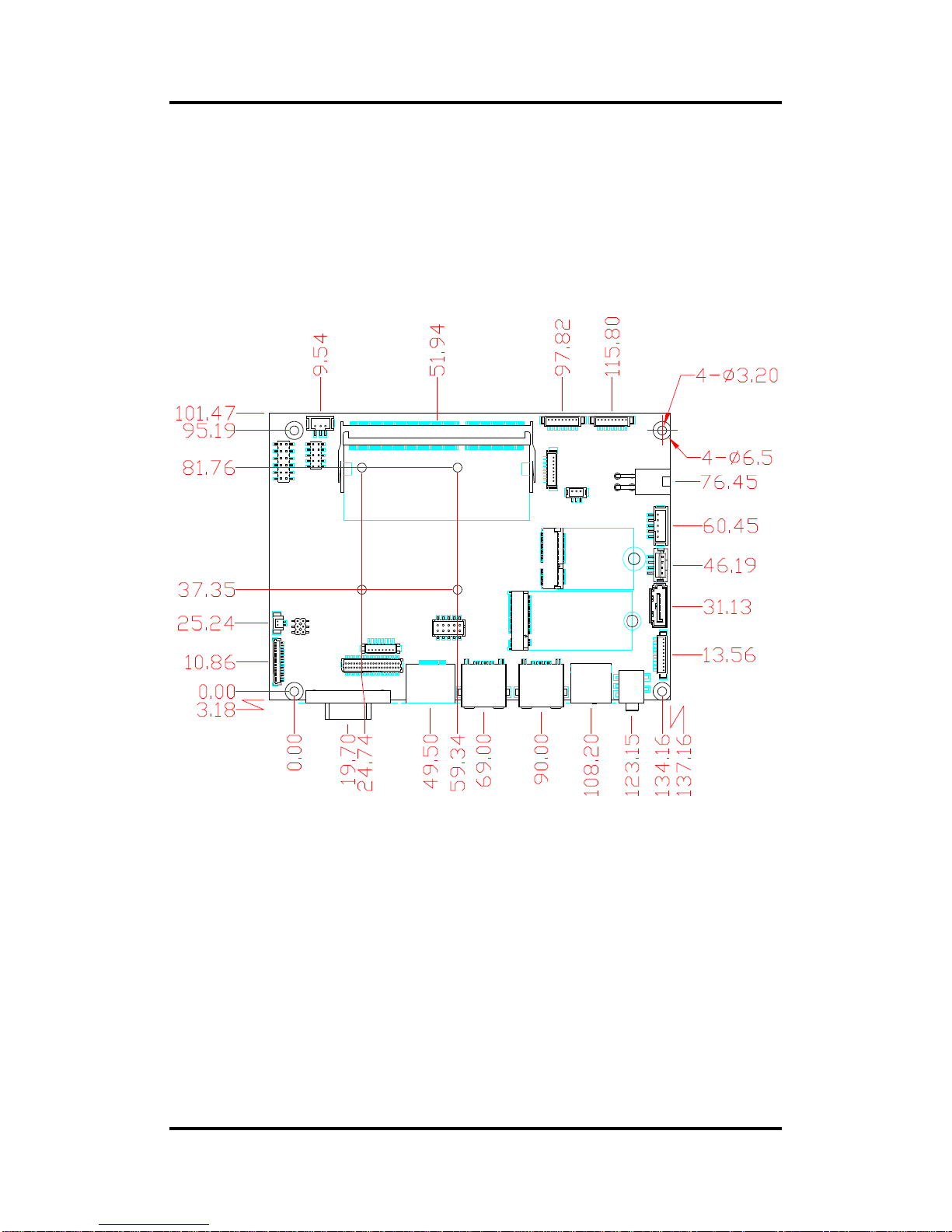
2.1 Board Dimensions and Fixing Holes
Top View
Page 12
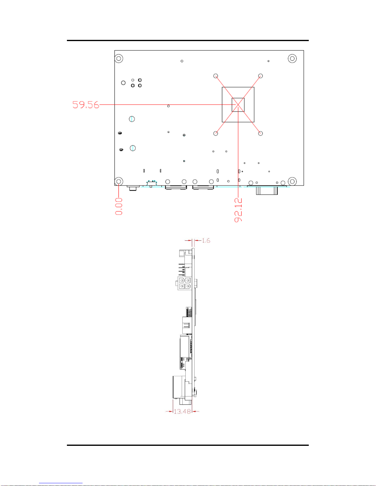
CAPA84R Capa Board
6 Board and Pin Assignments
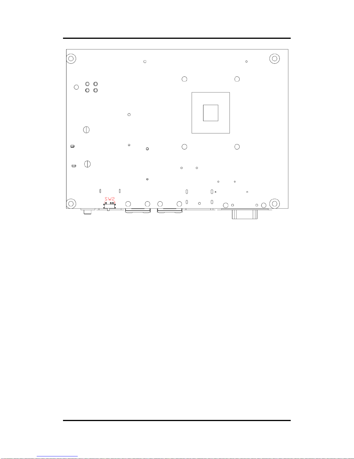
Bottom View
Side View
Page 13
CAPA84R Capa Board
Board and Pin Assignments 7
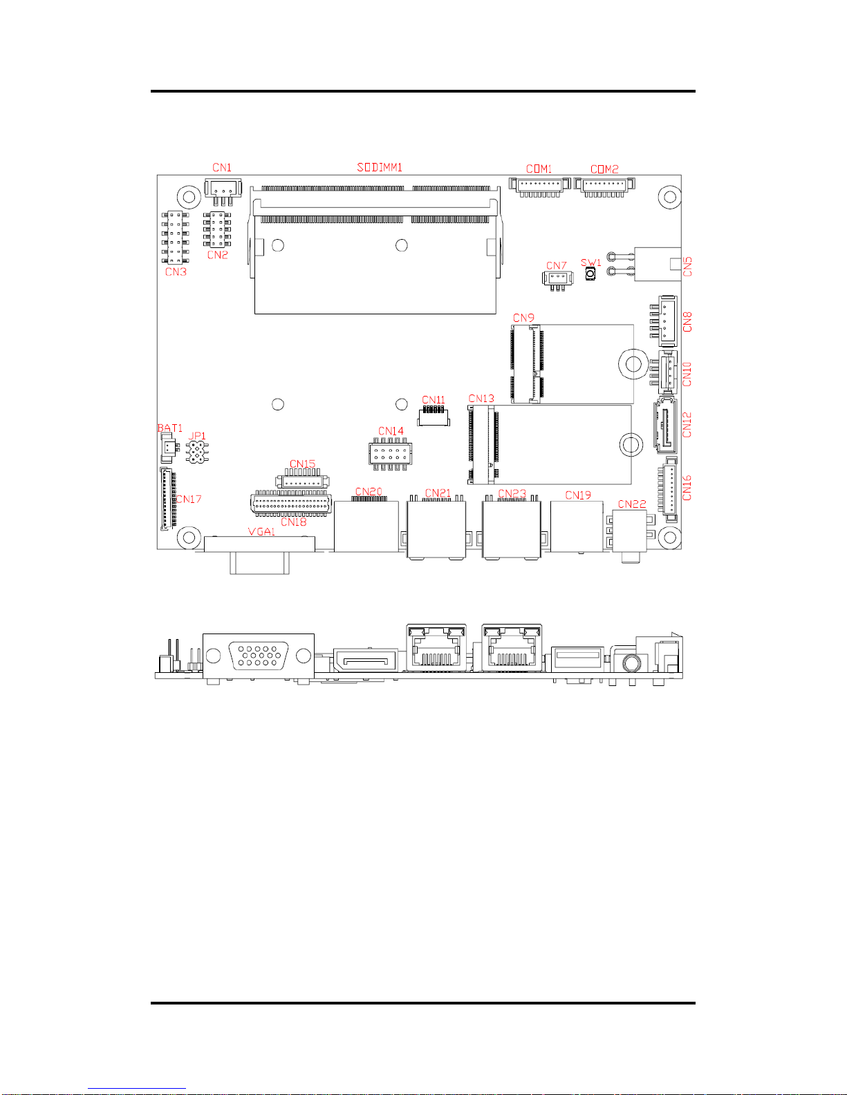
2.2 Board Layout
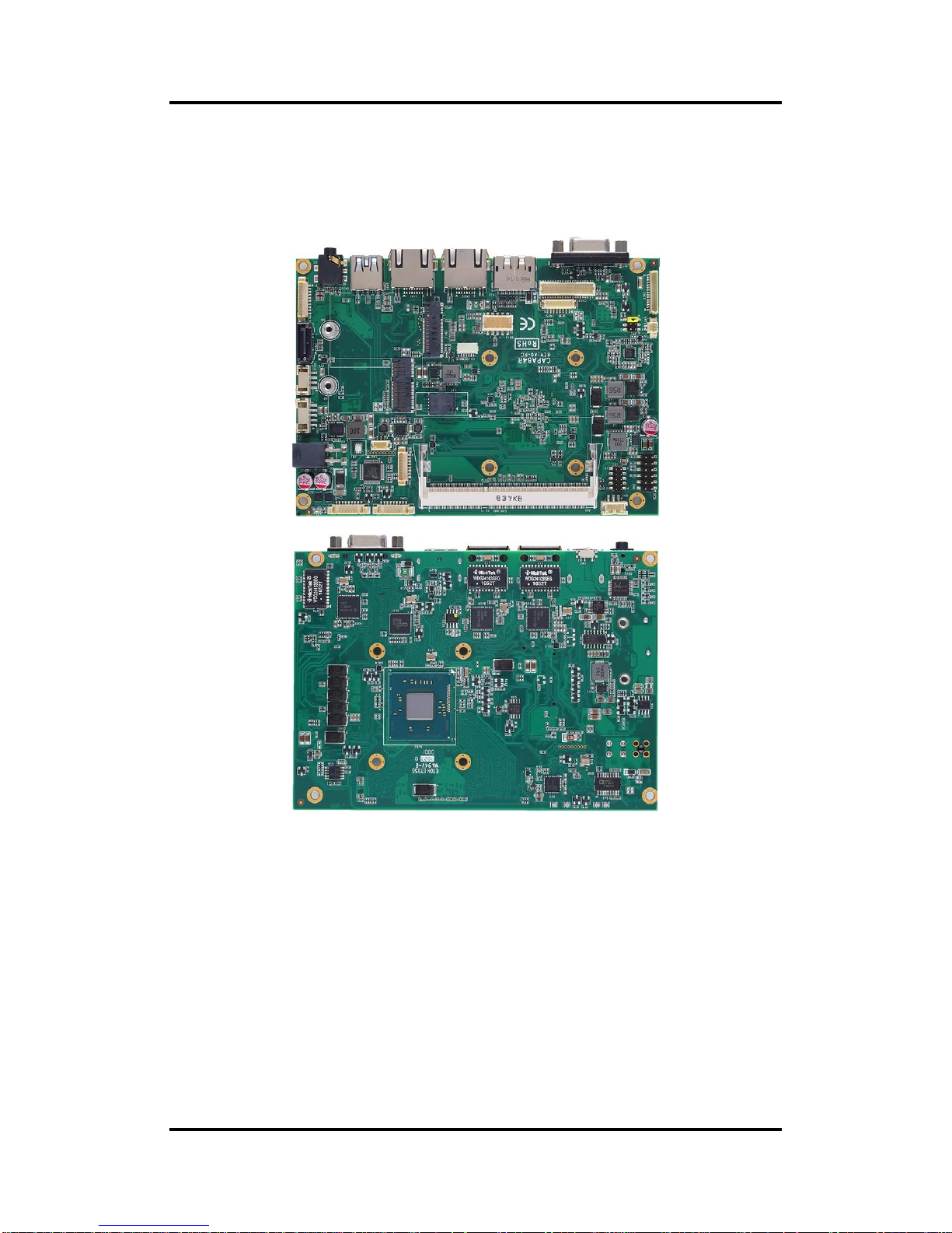
Top View
Side View
Page 14
CAPA84R Capa Board
8 Board and Pin Assignments
Bottom View
Page 15
CAPA84R Capa Board
Board and Pin Assignments 9
2.3 Jumper and Switch Settings
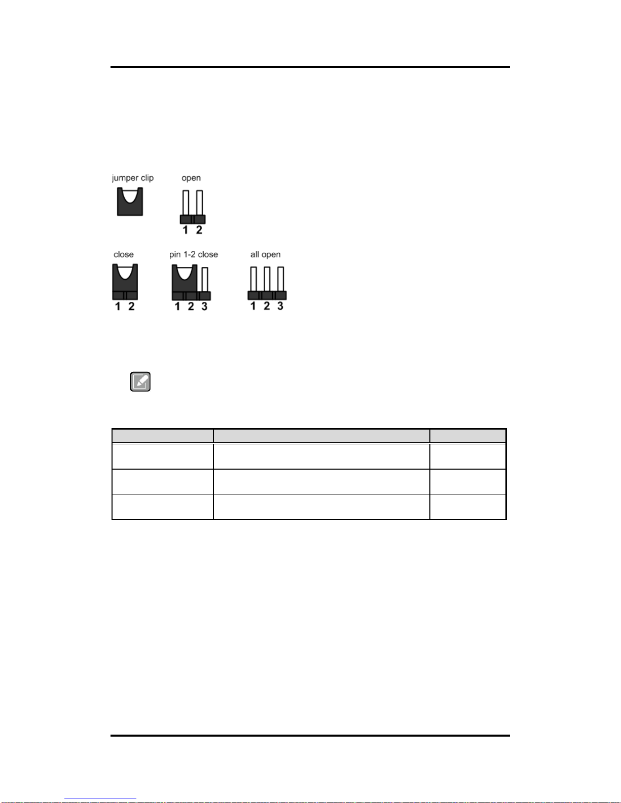
Jumper is a small component consisting of jumper clip and jumper pins. Install jumper clip on 2
jumper pins to close. And remove jumper clip from 2 jumper pins to open. Below illustration
shows how to set up jumper.
Properly configure jumper and switch settings on the CAPA84R to meet your application
purpose. Below you can find a summary table of jumpers, switch and onboard default settings.
Note
Once the default jumper or switch setting needs to be changed, please do it under
power-off condition.
Jumper and Switch
Description
Setting
JP1
LVDS Voltage Selection
Default: +3.3V Level
1-2 Close
SW1
Restore BIOS Optimal Defaults
Default: Normal Operation
Release
SW2
Auto Power On
Default: Disable
1-2 Close
Page 16
CAPA84R Capa Board
10 Board and Pin Assignments
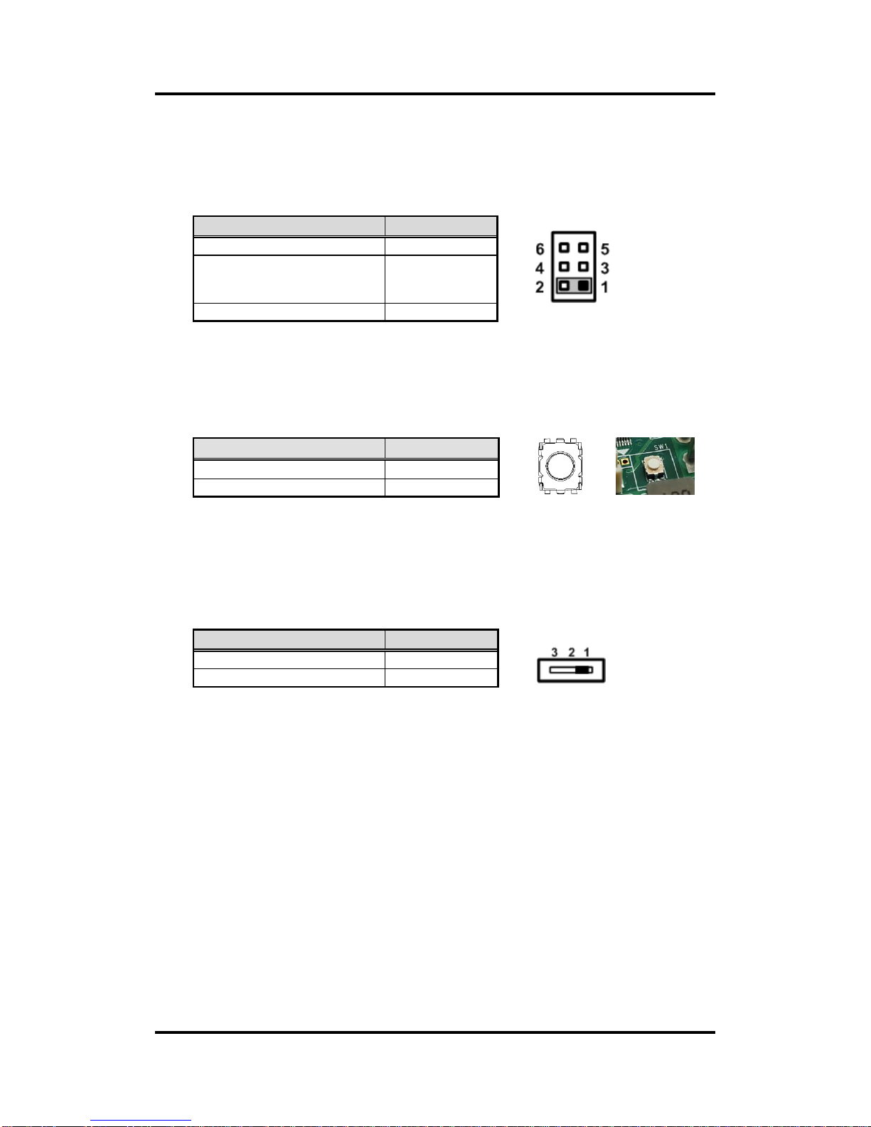
2.3.1 LVDS Voltage Selection (JP1)
This is a 2x3-pin (pitch=2.0mm) jumper. The board supports voltage selection for flat
panel displays. Use JP1 to set LVDS connector (CN18) pin 1~6 VCCM to +3.3V, +5V or
+12V voltage level. To prevent hardware damage, before connecting please make sure
that input voltage of the flat panel is correct.
2.3.2 Restore BIOS Optimal Defaults (SW1)
Use SW1 to clear CMOS. Press the tact switch for at least 1 second to restore BIOS
optimal defaults.
2.3.3 Auto Power On (SW2)
If SW2 is enabled for power input, the system will be automatically power on without
pressing soft power button. If SW2 is disabled for power input, it is necessary to
manually press soft power button to power on the system.
Function
Setting
+3.3V level (Default)
1-2 close
+5V level
2-4 close
Or
4-6 close
+12V level
5-6 close
Function
Setting
Normal (Default)
Release
Restore BIOS optimal defaults
Press
Function
Setting
Disable auto power on (Default)
1-2 close
Enable auto power on
2-3 close
Page 17

CAPA84R Capa Board
Board and Pin Assignments 11
2.4 Connectors
Signals go to other parts of the system through connectors. Loose or improper connection
might cause problems, please make sure all connectors are properly and firmly connected.
Here is a summary table of connectors on the hardware.
Connector
Description
CN1
SMBus Connector
CN2
Digital I/O Connector
CN3
Front Panel Connector
CN5/ATX1
DC +12V Power Input Connector
CN7
Fan Connector
CN8
DC +5V/15W Power Output Connector
CN9
M.2 2230 Key E Connector
CN10
SATA Power Connector
CN11
SIM Card Wafer Connector
CN12
SATA Connector
CN13
M.2 2242/3042 Key B Connector
CN14
USB 2.0 Port 1 and 2 Wafer Connector
CN15
Inverter Connector
CN16
Audio Line-in/Line-out/Mic-in Wafer Connector
CN17
Ethernet Port 3 Wafer Connector
CN18
LVDS Connector
CN19
USB 3.0/2.0 Port 0 Type A Connector
CN20
DisplayPort Connector
CN21, CN23
Ethernet Port 1 and 2
CN22
Audio Line-out Phone Jack
VGA1
VGA Connector
COM1, COM2
COM1 and COM2 Wafer Connector
BAT1
CMOS Battery Connector
SODIMM1
DDR3L SO-DIMM Connector
Page 18
CAPA84R Capa Board
12 Board and Pin Assignments
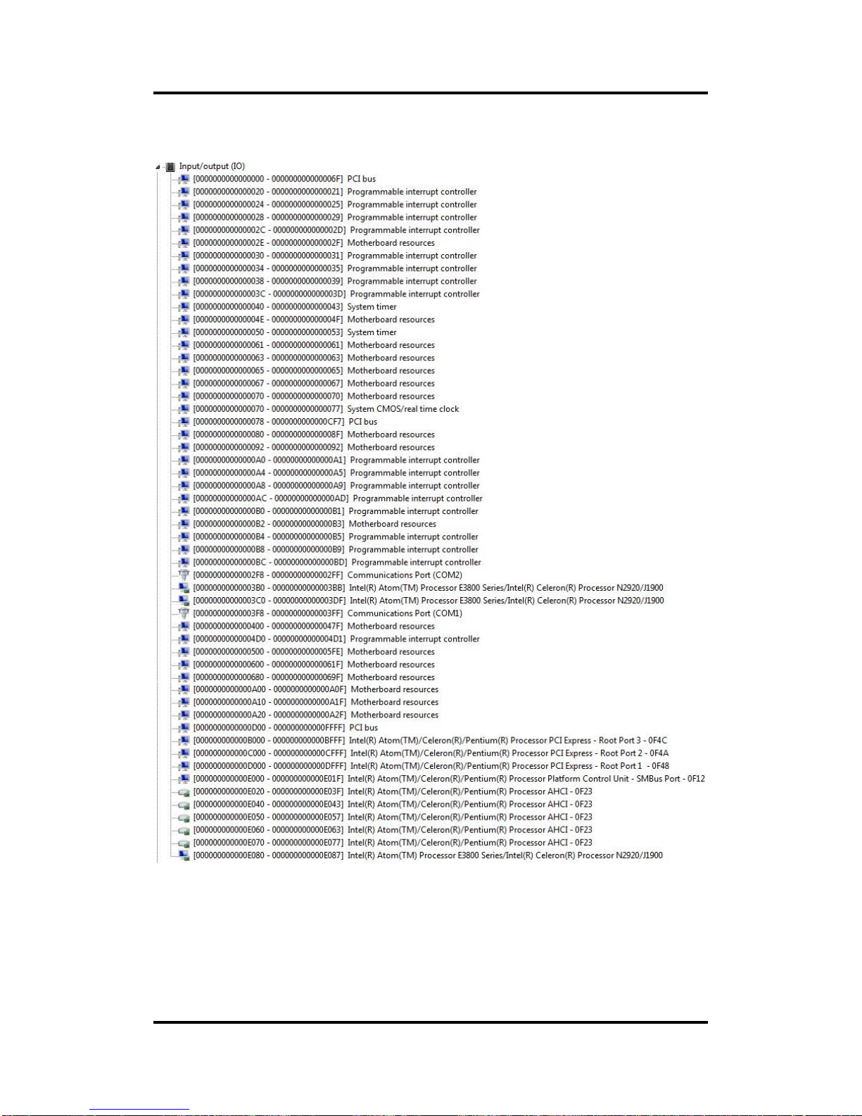
2.4.1 SMBus Connector (CN1)
This is a 3-pin (pitch=2.0mm) wafer connector which is compliant with JST
B4B-PH-SM3-TB for SMbus interface. The SMBus (System Management Bus) is a
simple bus for the purpose of lightweight communication.
1
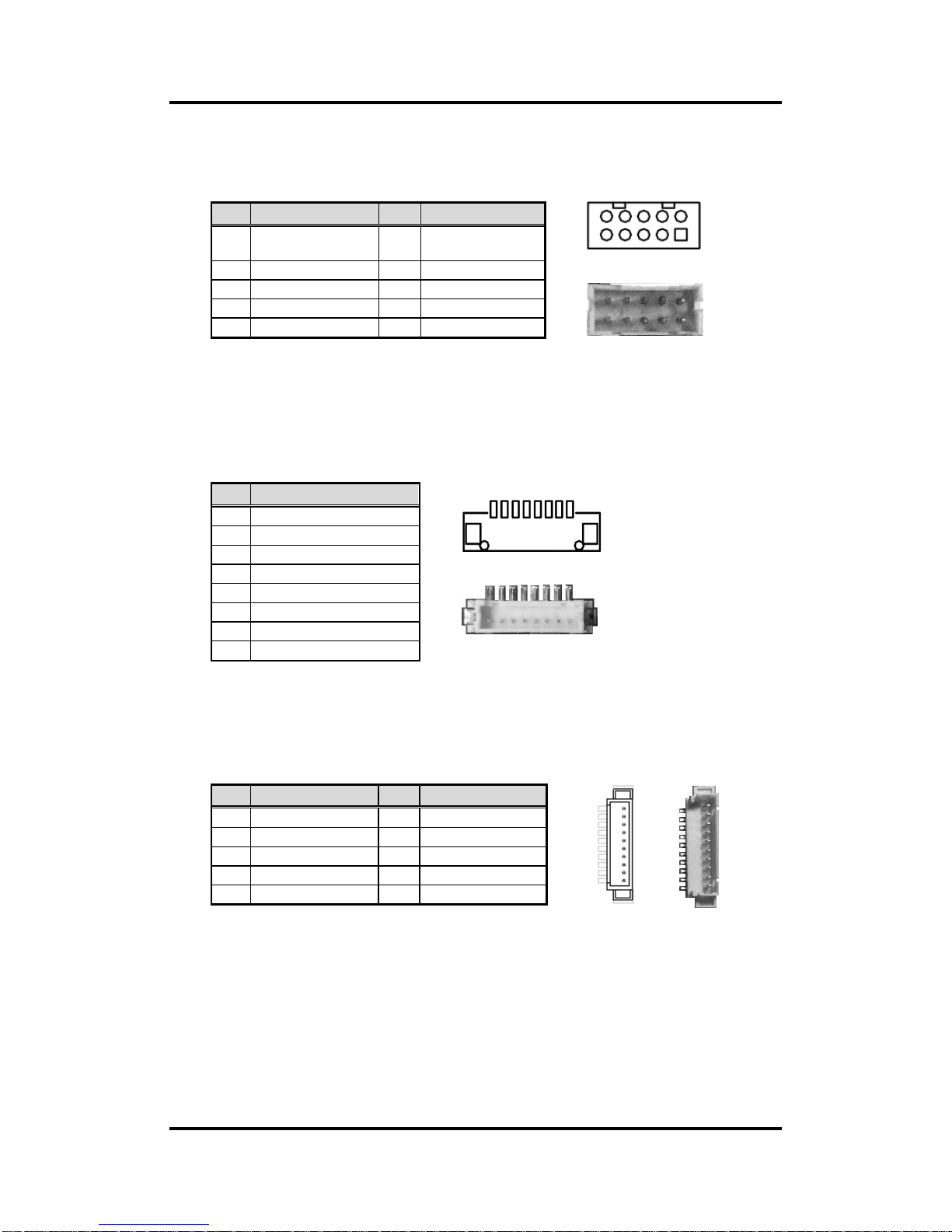
2.4.2 Digital I/O Connector (CN2)
This is a 2x5-pin (pitch=2.0mm) connector. The board is equipped with an 8-bit digital
I/O that meets requirements for a system customary automation control. The digital I/O
can be configured to control cash drawers and sense warning signals from an
Uninterrupted Power System (UPS), or perform store security control. You may use
software programming to control these digital signals, please refer to Appendix B.
Pin
Signal
1
CLK 2 DATA
3
GND
Pin
Signal
Pin
Signal
1
Digital Input Output 0
(Default: Output)
2
Digital Input Output 7
(Default: Input)
3
Digital Input Output 1
(Default: Output)
4
Digital Input Output 6
(Default: Input)
5
Digital Input Output 2
(Default: Output)
6
Digital Input Output 5
(Default: Input)
7
Digital Input Output 3
(Default: Output)
8
Digital Input Output 4
(Default: Input)
9
+5V level
10
GND
Page 19
CAPA84R Capa Board
Board and Pin Assignments 13
2.4.3 Front Panel Connector (CN3)
This is a 2x5-pin header (pitch=2.0mm) for front panel interface.
External Speaker
Pin 1(-) and 2(+) connect the case-mounted speaker unit or internal buzzer cable.
Power Status
Pin 4 and pin 3 are for power status button; letting user know the power status of this
board.
Power LED
Pin 6 connects anode (+) of LED and pin 5 connects cathode (-) of LED. The power LED
lights up when the system is powered on.
Power On/Off Button
Pin 8 and 7 connect the power button on front panel to CPU board, which allows users to
turn on or off power supply.
System Reset Switch
Pin 10 and 9 connect the case-mounted reset switch that reboots your computer without
turning off the power switch. It is a better way to reboot your system for a longer life of
system power supply.
HDD Activity LED
This connection is linked to hard drive activity LED on the control panel. LED flashes
when HDD is being accessed. Pin 12 and 11 connect the hard disk drive to the front
panel HDD LED, pin 11 is assigned as cathode(-) and pin 12 is assigned as anode(+).
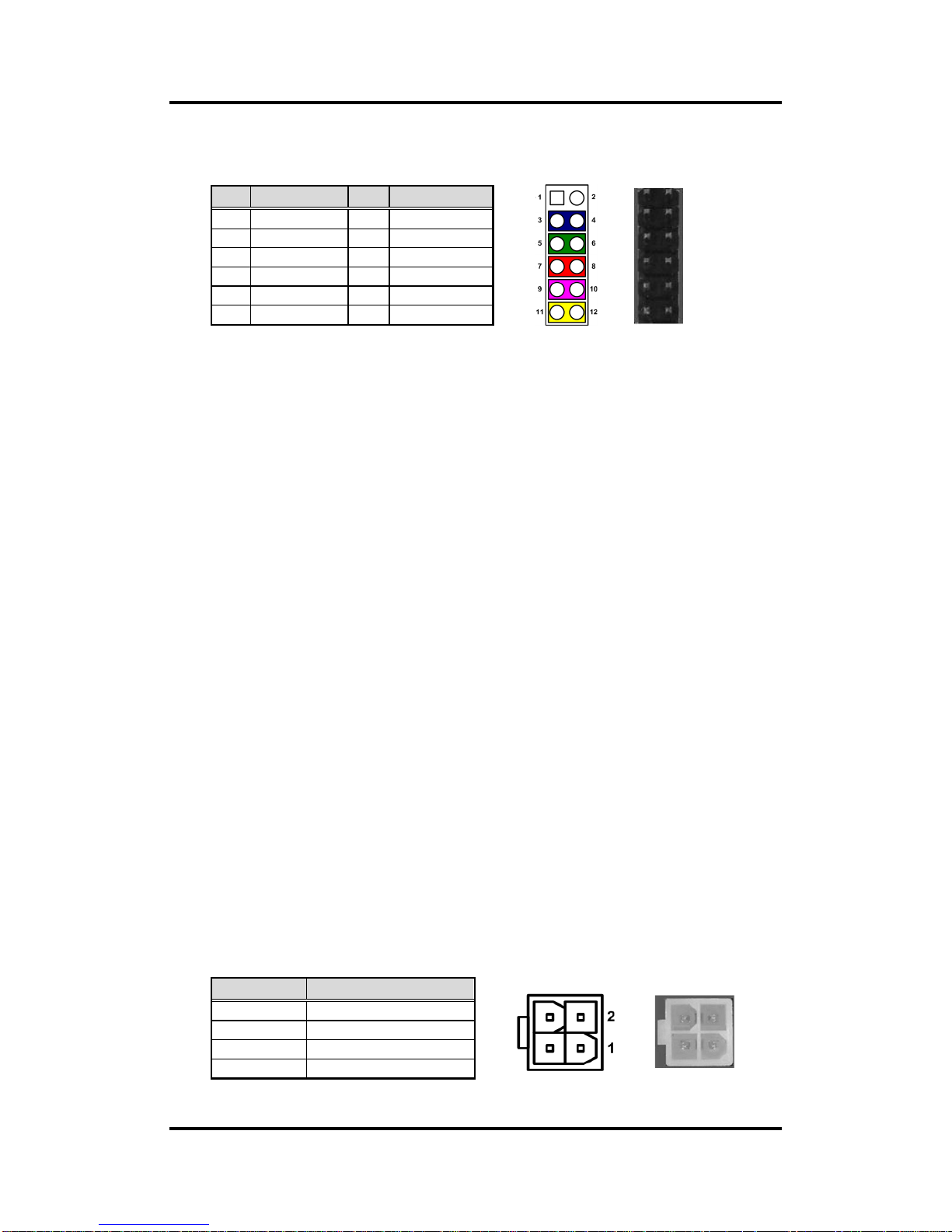
2.4.4 DC +12V Power Input Connector (CN5/ATX1)
Steady and sufficient power can be supplied to all components on the board by
connecting the power connector. Please make sure all components and devices are
properly installed before connecting the power connector.
The CN5/ATX1 is a 4-pin DC +12V power input interface. The CN5 is in right angle while
the ATX1 is in vertical position. Follow the connector orientation to plug the external
power supply. Properly press down power supply plug until it completely and firmly fits
into this connector. Loose connection may cause system instability.
Pin
Signal
Pin
Signal
1
EXT SPK-
2
EXT SPK+
3
GND
4
PWR_PSON
5
PWRLED-
6
PWRLED+
7
PWRSW-
8
PWRSW+
9
HW RST-
10
HW RST+
11
HDDLED-
12
HDDLED+
Pin
Signal
1
GND
2
GND
3
+12V
4
+12V
Page 20
CAPA84R Capa Board
14 Board and Pin Assignments
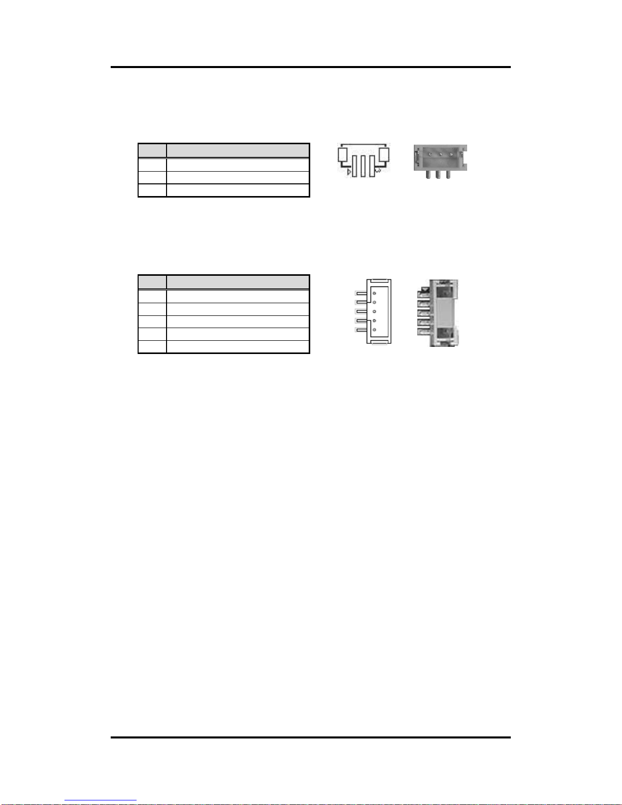
2.4.5 Fan Connector (CN7)
This is a 3-pin (pitch=1.5mm) connector. A fan interface is available through CN7. You
can find fan speed within BIOS Setup Utility if fan is installed. For further information,
see BIOS Setup Utility: Advanced\Hardware Monitor\PC Health Status in section 4.4.
2.4.6 DC +5V/15W Power Output Connector (CN8)
The CN8 is a 5-pin (pitch=2mm) wafer connector, which is compliant with JST
B5B-PH-K-S.
Pin
Signal
1
GND
2
+12V level
3
Fan speed feedback
Pin
Signal
1
GND
2
GND
3
GND
4
+5V 5 +5V
1
1
5
Page 21
CAPA84R Capa Board
Board and Pin Assignments 15
2.4.7 M.2 2230 Key E Connector (CN9)
The CN9 is a M.2 2230 Key E connector.
It is suggested to install the M.2 wireless module via PCIex1 with 22mm width and 30mm
length.
Pin
Signal
Pin
Signal
1
GND
2
+3.3V_SBY
3
NC 4 +3.3V_SBY
5
NC 6 NC 7 GND
8
NC 9 NC
10
NC
11
NC
12
NC
13
NC
14
NC
15
NC
16
NC
17
NC
18
GND
19
NC
20
NC
21
NC
22
NC
23
NC
24
Key E
25
Key E
26
27
28
29
30
31
32
NC
33
GND
34
NC
35
PCIE3_TX_P
36
NC
37
PCIE3_TX_N
38
NC
39
GND
40
NC
41
PCIE3_RX_P
42
NC
43
PCIE3_RX_N
44
NC
45
GND
46
NC
47
CLK_PCIE3_P
48
NC
49
CLK_PCIE3_N
50
SUSCLK(+3.3V Level)
51
GND
52
PERST#(+3.3V Level)
53
CLKREQ0#
54
W_DIS2#(+3.3V Level)
55
PEWAKE0#
56
W_DI12#(+3.3V Level)
57
GND
58
SMB_DATA(+3.3V
Level)
59
NC
60
SMB_CLK(+3.3V
Level)
61
NC
62
ALERT#(+3.3V Level)
63
GND
64
NC
65
NC
66
NC
67
NC
68
NC
69
GND
70
NC
71
NC
72
+3.3V_SBY
73
NC
74
+3.3V_SBY
75
GND
Page 22
CAPA84R Capa Board
16 Board and Pin Assignments
2.4.8 SATA Power Connector (CN10)
This is a 4-pin (pitch=2mm) wafer connector, which is compliant with JST B4B-PH-K-S,
for SATA power interface.
2.4.9 SIM Card Wafer Connector (CN11)
The CN11 is a 6-pin (pitch=1.0mm) wafer connector, which is compliant with JST
B6B-PH-K-S, for SIM Card interface. AX93A19 is suggested to use for CN11 to have
SIM card slot.
In order to work properly, the SIM card must be used together with 3G/LTE module in
M.2 Key B connector/CN13. It is mainly used in 3G/LTE wireless network application.
2.4.10 SATA Connector (CN12)
This Serial Advanced Technology Attachment (Serial ATA or SATA) connector is for
high-speed SATA interface. It is a computer bus interface for connecting to devices such
as hard disk drive.
Pin
Signal
1
+12V
2
GND
3
GND
4
+5V
Pin
Signal
1
PWR
2
RESET
3
CLK 4 DAT 5 VPP 6 GND
Pin
Signal
1
GND
2
SATA0_TXP
3
SATA0_TXN
4
GND
5
SATA0_RXN
6
SATA0_RXP
7
GND
1
7
1
Page 23
CAPA84R Capa Board
Board and Pin Assignments 17
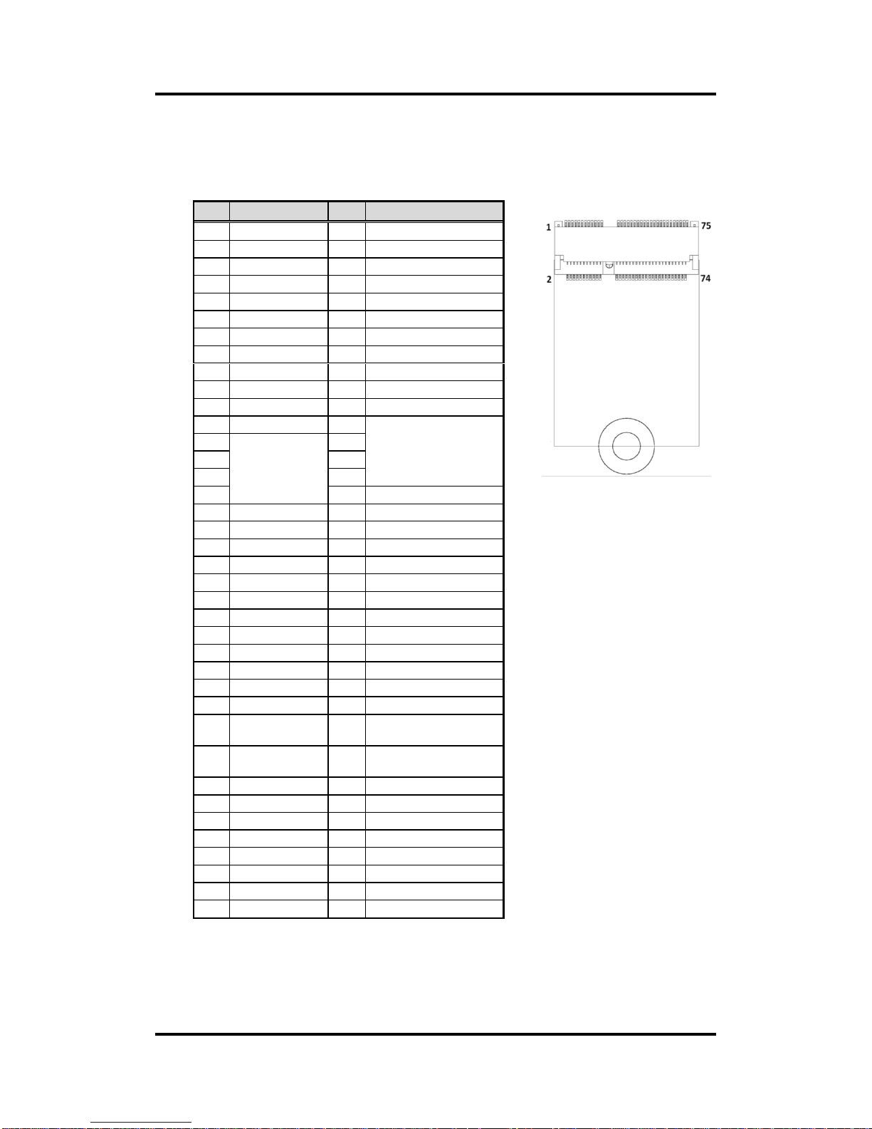
2.4.11 M.2 2242/3042 Key B Connector (CN13)
The CN13 is a M.2 Key B connector. It is suggested to install the M.2 storage module via
SATA with 22mm width and 42mm length or the M.2 cellular module via USB 2.0 with
30mm width and 42mm length.
Pin
Signal
Pin
Signal
1
CONFIG_3
2
+3.3V_SBY
3
GND
4
+3.3V_SBY
5
GND
6
Full Card PWR OFF
7
USB_D3+
8
W_DISABLE#
9
USB_D3-
10
NC
11
GND
12
Key B
13
Key B
14
15
16
17
18
19
20
NC
21
CONFIG_0
22
NC
23
GPIO11(+1.8V)
24
NC
25
NC
26
NC
27
GND
28
NC
29
NC
30
SMB_RST
31
NC
32
SMB_CLK
33
GND
34
SMB_DATA
35
NC
36
SMB_PWR
37
NC
38
NC
39
GND
40
SMB_CLK_SBY(+1.8V)
41
SATA1_RX_P
42
SMB_DATA_SBY(+1.8V)
43
SATA1_RX_N
44
SMB_CLK_ALRT(+1.8V)
45
GND
46
NC
47
SATA1_TX_N
48
NC
49
SATA1_RX_P
50
PERST#
51
GND
52
CLKREQ#
53
NC
54
PEWAKE#
55
NC
56
NC
57
GND
58
NC
59
NC
60
NC
61
NC
62
NC
63
NC
64
NC
65
NC
66
NC
67
PLTRST
68
SUSCLK
69
CONFIG_1
70
+3.3V_SBY
71
GND
72
+3.3V_SBY
73
GND
74
+3.3V_SBY
75
CONFIG_2
Page 24
CAPA84R Capa Board
18 Board and Pin Assignments
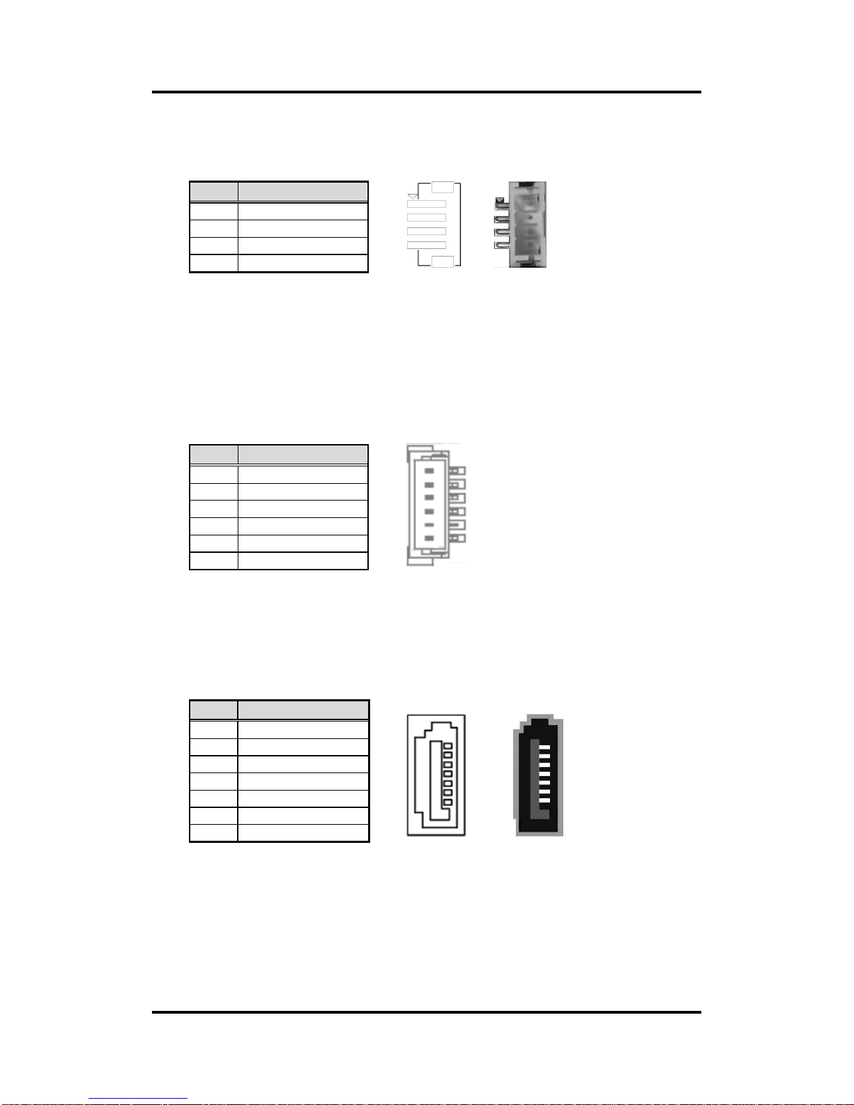
2.4.12 USB 2.0 Wafer Connector (CN14)
This is a 2x5-pin (pitch=2mm) wafer connector, which is compliant with Hirose
DF11-xdp-2dsa, for installing versatile USB 2.0 compliant interface peripherals.
9 1
2.4.13 Inverter Connector (CN15)
This is an 8-pin (pitch=1.25mm) connector, which is compliant with Hirose
DF13-8P-1.25V, for inverter interface. We strongly recommend you to use the matching
connector, DF13-8S-1.25C, to avoid malfunction.
1 8
2.4.14 Audio Wafer Connector (CN16)
This is a 10-pin (pitch=1.25mm) wafer connector, which is compliant with Molex
53047-1010, for line-in/line-out/MIC-in interface.
Pin
Signal
Pin
Signal
1
USB VCC
(+5V_SBY)
2
USB VCC
(+5V_SBY)
3
USB #1_D-
4
USB #2_D-
5
USB #1_D+
6
USB #2_D+
7
GND
8
GND
9
GND
10
GND
Pin
Signal
1
VBL1 (+12V level)
2
VBL1 (+12V level)
3
VBL2 (+5V level)
4
VBL_ENABLE
5
GND
6
GND
7
GND
8
VBL Brightness Control
Pin
Signal
Pin
Signal
1
MIC_IN
2
GND
3
LINE_IN_L
4
GND
5
LINE_IN_R
6
GND
7
AUDIO_OUT_L
8
GND
9
AUDIO_OUT_R
10
GND
1
Page 25

CAPA84R Capa Board
Board and Pin Assignments 19
2.4.15 Ethernet Wafer Connector (CN17)
This is a JST BM16B-SRSS-TB 15-pin (pitch=1.0mm) wafer connector for Ethernet port
3 interface.
Pin
Signal
1
LAN_1000_LED
2
LAN_100_LED
3
GND
4
MDI3-
5
MDI3+
6
MDI1-
7
MDI2-
8
MDI2+
9
MDI1+
10
MDI0-
11
MDI0+
12
GND
13
LAN_VDD33
14
LAN_LINK_ACT
15
GND
1
15
Page 26

CAPA84R Capa Board
20 Board and Pin Assignments
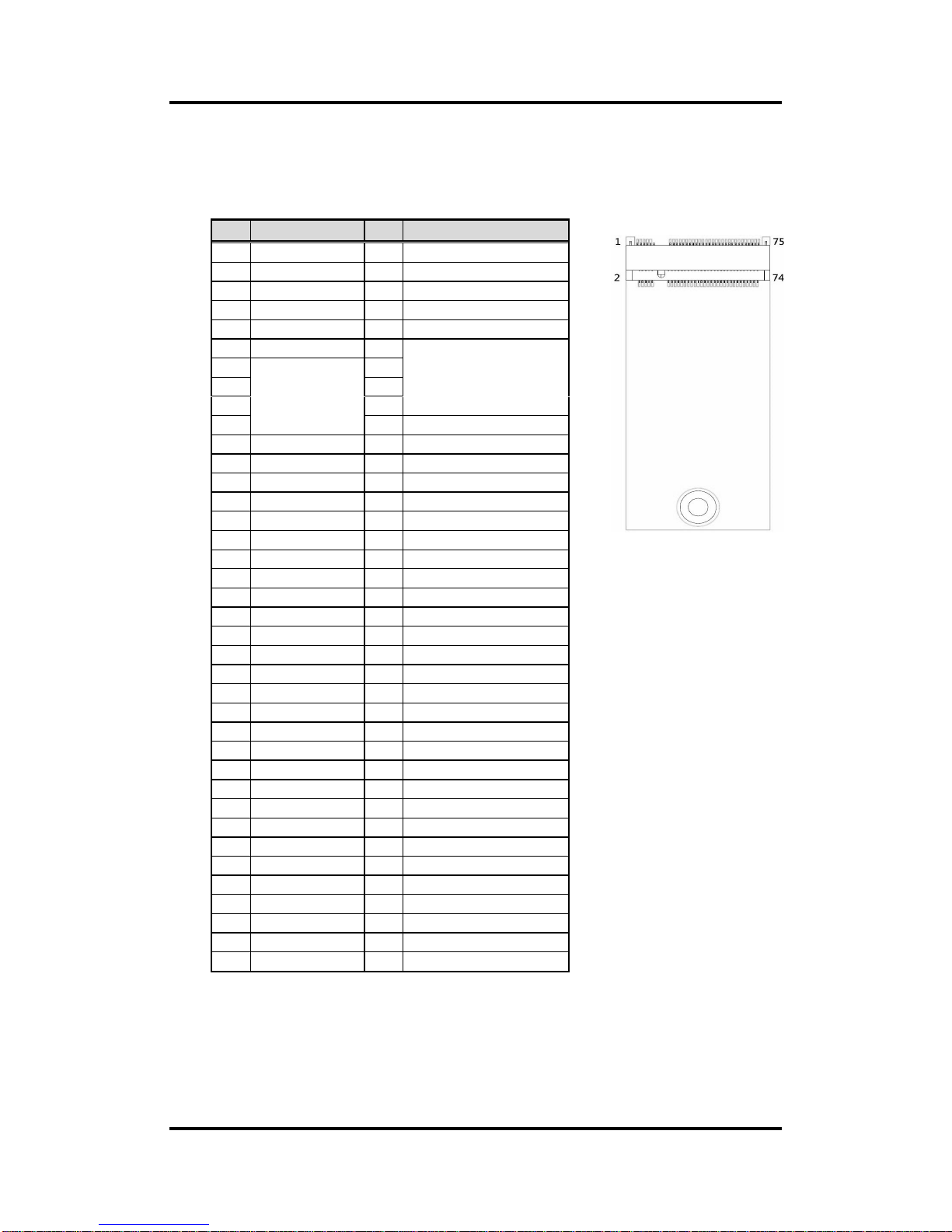
2.4.16 LVDS Connector (CN18)
This board has one 2x20-pin (pitch=1mm) connector for LVDS LCD interface. It is
strongly recommended to use the matching JST SHDR-40VS-B connector for LVDS
interface. Pin 1~6 VCCM can be set to +3.3V, +5V or +12V by setting JP1 (see section
2.3.1).
18-bit single channel
Pin
Signal
Pin
Signal
1
VCCM
2
VCCM
3
VCCM
4
VCCM
5
VCCM
6
VCCM
7
N.C 8 N.C 9 GND
10
GND
11
N.C
12
N.C
13
N.C
14
N.C
15
GND
16
GND
17
N.C
18
N.C
19
N.C
20
N.C
21
GND
22
GND
23
Channel A D0-
24
N.C
25
Channel A D0+
26
N.C
27
GND
28
GND
29
Channel A D1-
30
N.C
31
Channel A D1+
32
N.C
33
GND
34
GND
35
Channel A D2-
36
Channel A CLK-
37
Channel A D2+
38
Channel A CLK+
39
GND
40
GND
Page 27

CAPA84R Capa Board
Board and Pin Assignments 21
24-bit single channel 18-bit dual channel
Pin
Signal
Pin
Signal
Pin
Signal
Pin
Signal
1
VCCM
2
VCCM
1 VCCM
2
VCCM
3
VCCM
4
VCCM
3 VCCM
4
VCCM
5
VCCM
6
VCCM
5 VCCM
6
VCCM
7
N.C 8 N.C
7
N.C 8 N.C
9
GND
10
GND 9
GND
10
GND
11
N.C
12
N.C 11
N.C
12
Channel B D0-
13
N.C
14
N.C 13
N.C
14
Channel B D0+
15
GND
16
GND 15
GND
16
GND
17
N.C
18
N.C 17
Channel B CLK-
18
Channel B D1-
19
N.C
20
N.C 19
Channel B CLK+
20
Channel B D1+
21
GND
22
GND 21
GND
22
GND
23
Channel A D0-
24
N.C 23
Channel A D0-
24
Channel B D2-
25
Channel A D0+
26
N.C 25
Channel A D0+
26
Channel B D2+
27
GND
28
GND 27
GND
28
GND
29
Channel A D1-
30
Channel A D3-
29
Channel A D1-
30
N.C
31
Channel A D1+
32
Channel A D3+
31
Channel A D1+
32
N.C
33
GND
34
GND 33
GND
34
GND
35
Channel A D2-
36
Channel A CLK-
35
Channel A D2-
36
Channel A CLK-
37
Channel A D2+
38
Channel A CLK+
37
Channel A D2+
38
Channel A CLK+
39
GND
40
GND 39
GND
40
GND
24-bit dual channel
Pin
Signal
Pin
Signal
1
VCCM
2
VCCM
3
VCCM
4
VCCM
5
VCCM
6
VCCM
7
N.C
8
N.C
9
GND
10
GND
11
Channel B D3-
12
Channel B D0-
13
Channel B D3+
14
Channel B D0+
15
GND
16
GND
17
Channel B CLK-
18
Channel B D1-
19
Channel B CLK+
20
Channel B D1+
21
GND
22
GND
23
Channel A D0-
24
Channel B D2-
25
Channel A D0+
26
Channel B D2+
27
GND
28
GND
29
Channel A D1-
30
Channel A D3-
31
Channel A D1+
32
Channel A D3+
33
GND
34
GND
35
Channel A D2-
36
Channel A CLK-
37
Channel A D2+
38
Channel A CLK+
39
GND
40
GND
Page 28

CAPA84R Capa Board
22 Board and Pin Assignments
2.4.17 USB 3.0/2.0 Type A Connector (CN19)
The Universal Serial Bus (compliant with USB 3.0 (5Gb/s)) type A connector on the rear
I/O is for installing USB peripherals such as keyboard, mouse, scanner, etc.
2.4.18 DisplayPort Connector (CN20)
The DisplayPort interface is available through connector CN20.
Pin
Signal
1
USB_VCC (+5V)
2
USB #0_D-
3
USB #0_D+
4
GND
5
USB 3_SSRX0-
6
USB 3_SSRX0+
7
GND
8
USB 3_SSTX0-
9
USB 3_SSTX0+
Pin
Signal
1
DP_LANE0
2
GND
3
DP_LANE0#
4
DP_LANE1
5
GND
6
DP_LANE1#
7
DP_LANE2
8
GND
9
DP_LANE2#
10
DP_LANE3
11
GND
12
DP_LANE3#
13
Detect Pin
14
GND
15
DP_AUX
16
GND
17
DP_AUX#
18
DP_HPDE
19
GND
20
+3.3V
Page 29

CAPA84R Capa Board
Board and Pin Assignments 23
2.4.19 Ethernet Ports (CN21 and CN23)
The board has two RJ-45 Ethernet connectors, CN21 (for LAN2) and CN23 (for LAN1).
Connection can be established by plugging one end of the Ethernet cable into this
connector and the other end (phone jack) to a 1000/100/10-Base-T hub.
L1L2L3L4L5L6L7L8
A B
A B
2.4.20 Audio Line-out Phone Jack (CN22)
This is phone jack for audio out with HD audio support.
Install audio driver, and then attach audio device to
CN22.
2.4.21 VGA Connector (VGA1)
This is a standard 15-pin D-Sub connector commonly used for VGA display. This VGA
interface configuration can be configured via software utility.
Pin
1000
Base-T
100/10
Base-T
Description
L1
BI_DA+
TX+
Bidirectional or Transmit Data+
L2
BI_DA-
TX-
Bidirectional or Transmit Data-
L3
BI_DB+
RX+
Bidirectional or Receive Data+
L4
BI_DC+
N.C.
Bidirectional or Not Connected
L5
BI_DC-
N.C.
Bidirectional or Not Connected
L6
BI_DB-
RX-
Bidirectional or Receive Data-
L7
BI_DD+
N.C.
Bidirectional or Not Connected
L8
BI_DD-
N.C.
Bidirectional or Not Connected
A
Active Link LED
Off: No link
Blinking: Data activity detected
B
Speed LED
1000: Orange
100/10: Green/OFF
Pin
Signal
Pin
Signal
1
Red 2 Green
3
Blue 4 N.C. 5 GND
6
DETECT
7
GND
8
GND
9
VCC
10
GND
11
N.C.
12
DDC DATA
13
Horizontal Sync
14
Vertical Sync
15
DDC CLK
Page 30

CAPA84R Capa Board
24 Board and Pin Assignments
1
2.4.22 COM Wafer Connectors (COM1 and COM2)
These are 9-pin (pitch=1.25mm) connectors which are compliant with Molex
53047-0910. The pin assignments of RS-232/RS-422/RS-485 are listed in table below. If
you need COM1 port to support RS-422 or RS-485, please refer to BIOS setting in
section 4.4.
COM1:
COM2:
2.4.23 CMOS Battery Connector (BAT1)
This is a 2-pin (pitch=1.25mm) wafer connector for CMOS battery interface.
Pin
RS-232
RS-422
RS-485
1
DCD
TX-
Data-
2
RXD
TX+
Data+
3
TXD
RX+
No use
4
DTR
RX-
No use
5
GND
No use
No use
6
DSR
No use
No use
7
RTS
No use
No use
8
CTS
No use
No use
9
RI
No use
No use
Pin
RS-232
1
DCD
2
RXD
3
TXD 4 DTR 5 GND
6
DSR
7
RTS 8 CTS 9 RI
Pin
Signal
1
VBAT(+3V level)
2
GND
1
1
Page 31

CAPA84R Capa Board
Hardware Description 25
Chapter 3
Hardware Description
3.1 Microprocessors
The CAPA84R supports Intel® Celeron® J1900/J1800 processor which enables your system to
operate under Windows® 10 environments. The system performance depends on the
microprocessor. Make sure all correct settings are arranged for the installed microprocessor to
prevent the CPU from damages.
3.2 BIOS
The CAPA84R uses AMI Plug and Play BIOS with a single 16Mbit SPI Flash.
3.3 System Memory
The CAPA84R supports one 204-pin DDR3L SO-DIMM socket for maximum memory capacity
up to 8GB DDR3L SDRAMs. The memory module comes in sizes of 2GB, 4GB and 8GB.
Page 32
CAPA84R Capa Board
26 Hardware Description
3.4 I/O Port Address Map
Page 33

CAPA84R Capa Board
Hardware Description 27
3.5 Interrupt Controller (IRQ) Map
The interrupt controller (IRQ) mapping list is shown as follows:
Page 34

CAPA84R Capa Board
28 Hardware Description
Page 35

CAPA84R Capa Board
Hardware Description 29
3.6 Memory Map
The memory mapping list is shown as follows:
Page 36

CAPA84R Capa Board
30 Hardware Description
This page is intentionally left blank.
Page 37

CAPA84R Capa Board
AMI BIOS Setup Utility 31
Chapter 4
AMI BIOS Setup Utility
The AMI UEFI BIOS provides users with a built-in setup program to modify basic system
configuration. All configured parameters are stored in a flash chip to save the setup information
whenever the power is turned off. This chapter provides users with detailed description about
how to set up basic system configuration through the AMI BIOS setup utility.
4.1 Starting
To enter the setup screens, follow the steps below:
1. Turn on the computer and press the <Del> key immediately.
2. After you press the <Del> key, the main BIOS setup menu displays. You can access the
other setup screens from the main BIOS setup menu, such as the Advanced and Chipset
menus.
Note
If your computer cannot boot after making and saving system changes with BIOS
setup, you can restore BIOS optimal defaults by setting SW1 (see section 2.3.2).
It is strongly recommended that you should avoid changing the chipset’s defaults. Both AMI
and your system manufacturer have carefully set up these defaults that provide the best
performance and reliability.
4.2 Navigation Keys
The BIOS setup/utility uses a key-based navigation system called hot keys. Most of the BIOS
setup utility hot keys can be used at any time during the setup navigation process. These keys
include <F1>, <F2>, <Enter>, <ESC>, <Arrow> keys, and so on.
Note
Some of the navigation keys differ from one screen to another.
Page 38

CAPA84R Capa Board
32 AMI BIOS Setup Utility
Hot Keys
Description
Left/Right
The Left and Right <Arrow> keys allow you to select a setup screen.
Up/Down
The Up and Down <Arrow> keys allow you to select a setup screen or
sub-screen.
+ Plus/Minus
The Plus and Minus <Arrow> keys allow you to change the field value of a
particular setup item.
Tab
The <Tab> key allows you to select setup fields.
F1
The <F1> key allows you to display the General Help screen.
F2
The <F2> key allows you to Load Previous Values.
F3
The <F3> key allows you to Load Optimized Defaults.
F4
The <F4> key allows you to save any changes you have made and exit
Setup. Press the <F4> key to save your changes.
Esc
The <Esc> key allows you to discard any changes you have made and exit
the Setup. Press the <Esc> key to exit the setup without saving your
changes.
Enter
The <Enter> key allows you to display or change the setup option listed for a
particular setup item. The <Enter> key can also allow you to display the
setup sub- screens.
Page 39
CAPA84R Capa Board
AMI BIOS Setup Utility 33
4.3 Main Menu
When you first enter the setup utility, you will enter the Main setup screen. You can always
return to the Main setup screen by selecting the Main tab. System Time/Date can be set up as
described below. The Main BIOS setup screen is shown below.
BIOS Information
Display BIOS information.
System Language
Use this option to choose the system default language.
System Date/Time
Use this option to change the system time and date. Highlight System Time or System
Date using the <Arrow> keys. Enter new values through the keyboard. Press the <Tab>
key or the <Arrow> keys to move between fields. The date must be entered in MM/DD/YY
format. The time is entered in HH:MM:SS format.
Access Level
Display the access level of current user.
Page 40

CAPA84R Capa Board
34 AMI BIOS Setup Utility
4.4 Advanced Menu
The Advanced menu also allows users to set configuration of the CPU and other system
devices. You can select any of the items in the left frame of the screen to go to the sub menus:
► ACPI Settings
► F81803 Super IO Configuration
► Hardware Monitor
► Onboard DIO Configuration
► CPU Configuration
► IDE Configuration
► Miscellaneous Configuration
► USB Configuration
► Utility Configuration
For items marked with “”, please press <Enter> for more options.
Page 41
CAPA84R Capa Board
AMI BIOS Setup Utility 35
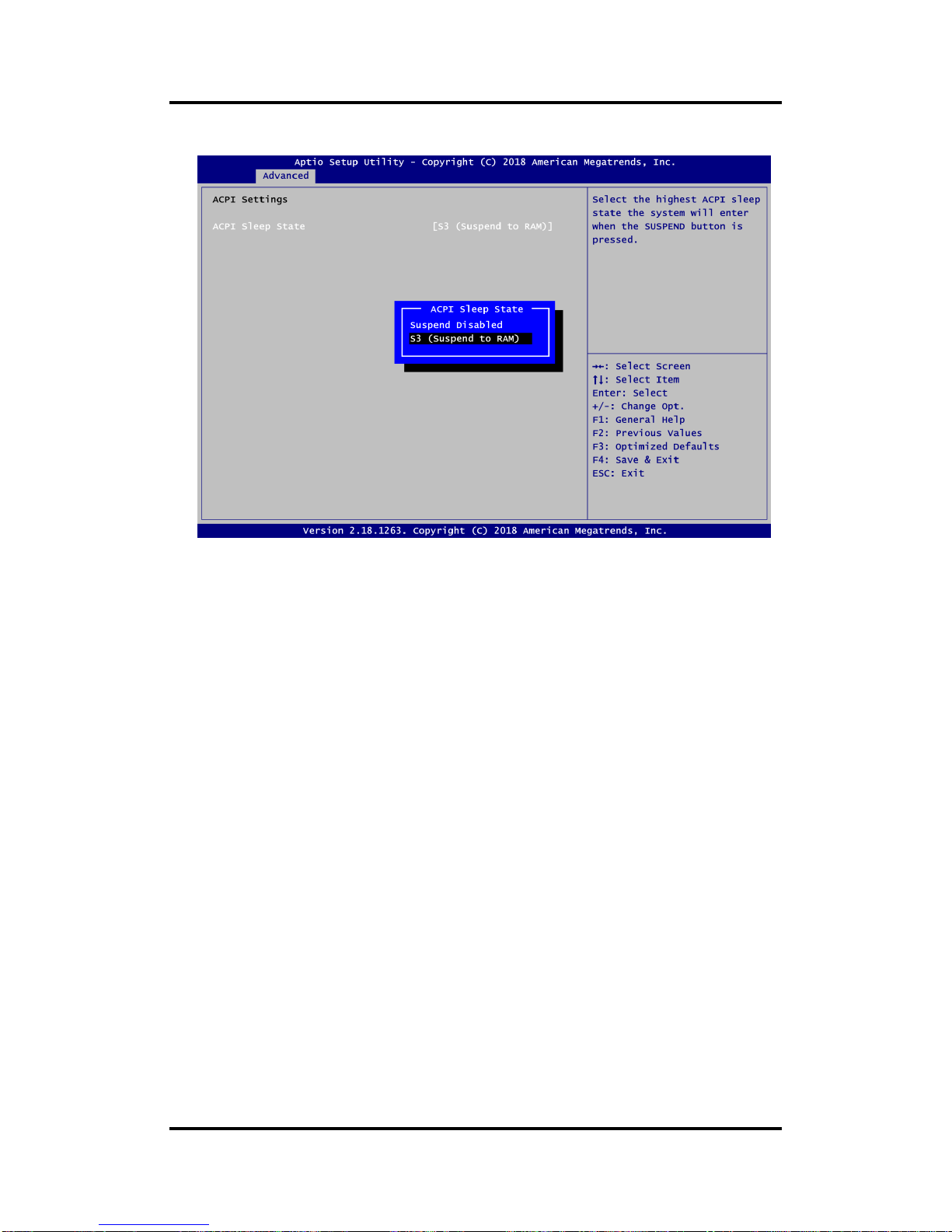
ACPI Settings
ACPI Sleep State
Select the ACPI (Advanced Configuration and Power Interface) sleep state. Configuration
options are Suspend Disabled and S3 (Suspend to RAM). The S3 (Suspend to RAM)
option selects ACPI sleep state the system will enter when suspend button is pressed.
Page 42

CAPA84R Capa Board
36 AMI BIOS Setup Utility
F81803 Super IO Configuration
You can use this screen to select options for serial port configuration, and change the
value of the selected option. A description of the selected item appears on the right side of
the screen. For items marked with “”, please press <Enter> for more options.
Serial Port 1~2 Configuration
Use these items to set parameters related to serial port 1~2.
Page 43
CAPA84R Capa Board
AMI BIOS Setup Utility 37
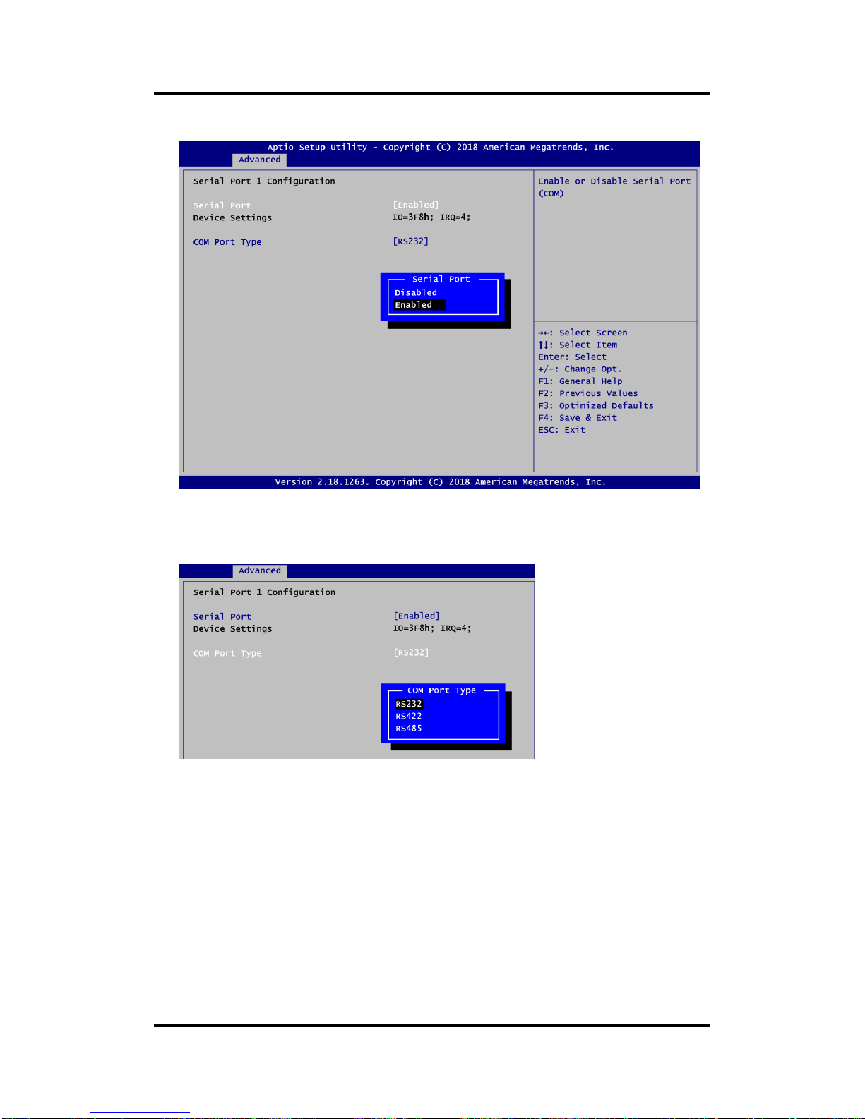
Serial Port 1 Configuration
Serial Port
Enable or disable serial port 1. The optimal setting for base I/O address is 3F8h and for
interrupt request address is IRQ4.
COM Port Type
Use this item to set RS-232/422/485 communication mode.
Page 44
CAPA84R Capa Board
38 AMI BIOS Setup Utility
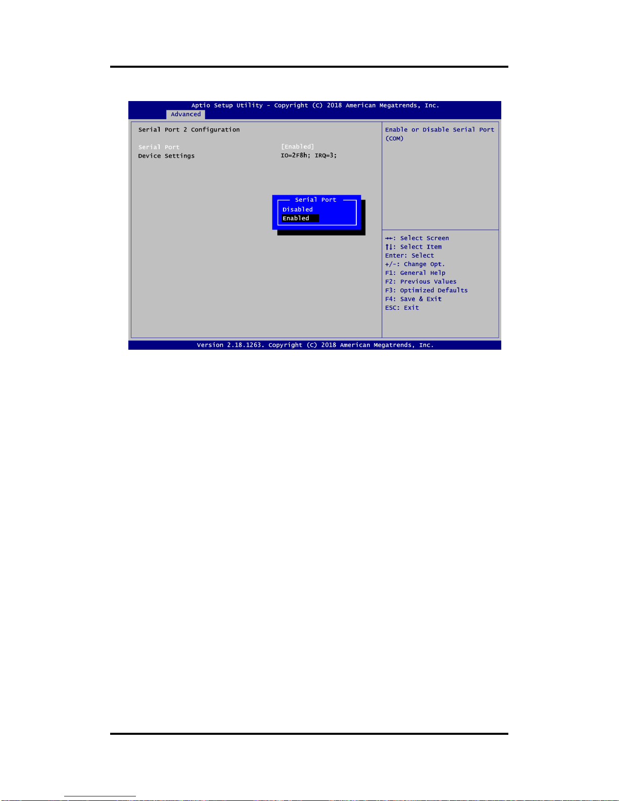
Serial Port 2 Configuration
Serial Port
Enable or disable serial port 2. The optimal setting for base I/O address is 2F8h and for
interrupt request address is IRQ3.
Page 45

CAPA84R Capa Board
AMI BIOS Setup Utility 39
Hardware Monitor
This screen monitors hardware health status.
This screen displays the temperature of system and CPU, fan speed in RPM and system
voltages (VBAT and +5V).
Page 46

CAPA84R Capa Board
40 AMI BIOS Setup Utility
Onboard DIO Configuration
You can use this screen to select options for the 8-bit Digital I/O Configuration. A
description of the selected item appears on the right side of the screen. For items marked
with “”, please press <Enter> for more options.
DIO Modification
Enable or disable digital I/O modification. The default is Disabled.
DIO port 1-8
Select this option to open DIO status sub screen.
Page 47

CAPA84R Capa Board
AMI BIOS Setup Utility 41
If DIO Modification is disabled, you are not allowed to change input/output setting. The
DIO status sub screen is as follows:
If DIO Modification is enabled, you can load manufacture default and access to the DIO
status sub screen to change input/output setting, see image below.
The DIO status sub screen is as follows:
Page 48
CAPA84R Capa Board
42 AMI BIOS Setup Utility
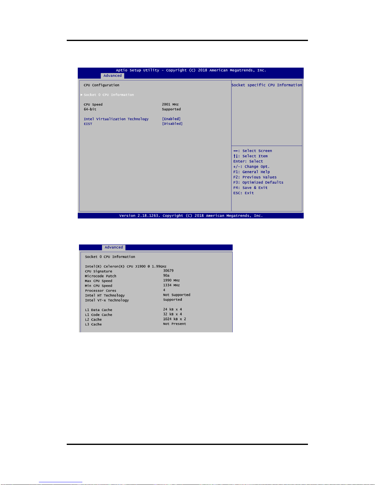
CPU Configuration
This screen shows the CPU Configuration.
Socket 0 CPU Information
Displays CPU information
Intel Virtualization Technology
Enable or disable Intel Virtualization Technology. When enabled, a VMM (Virtual Machine
Mode) can utilize the additional hardware capabilities. It allows a platform to run multiple
operating systems and applications independently, hence enabling a computer system to
work as several virtual systems.
EIST
Enable or disable Intel® SpeedStep. When disabled, CPU runs at its default speed. When
enabled, the CPU speed is controlled by the operating system.
Page 49
CAPA84R Capa Board
AMI BIOS Setup Utility 43
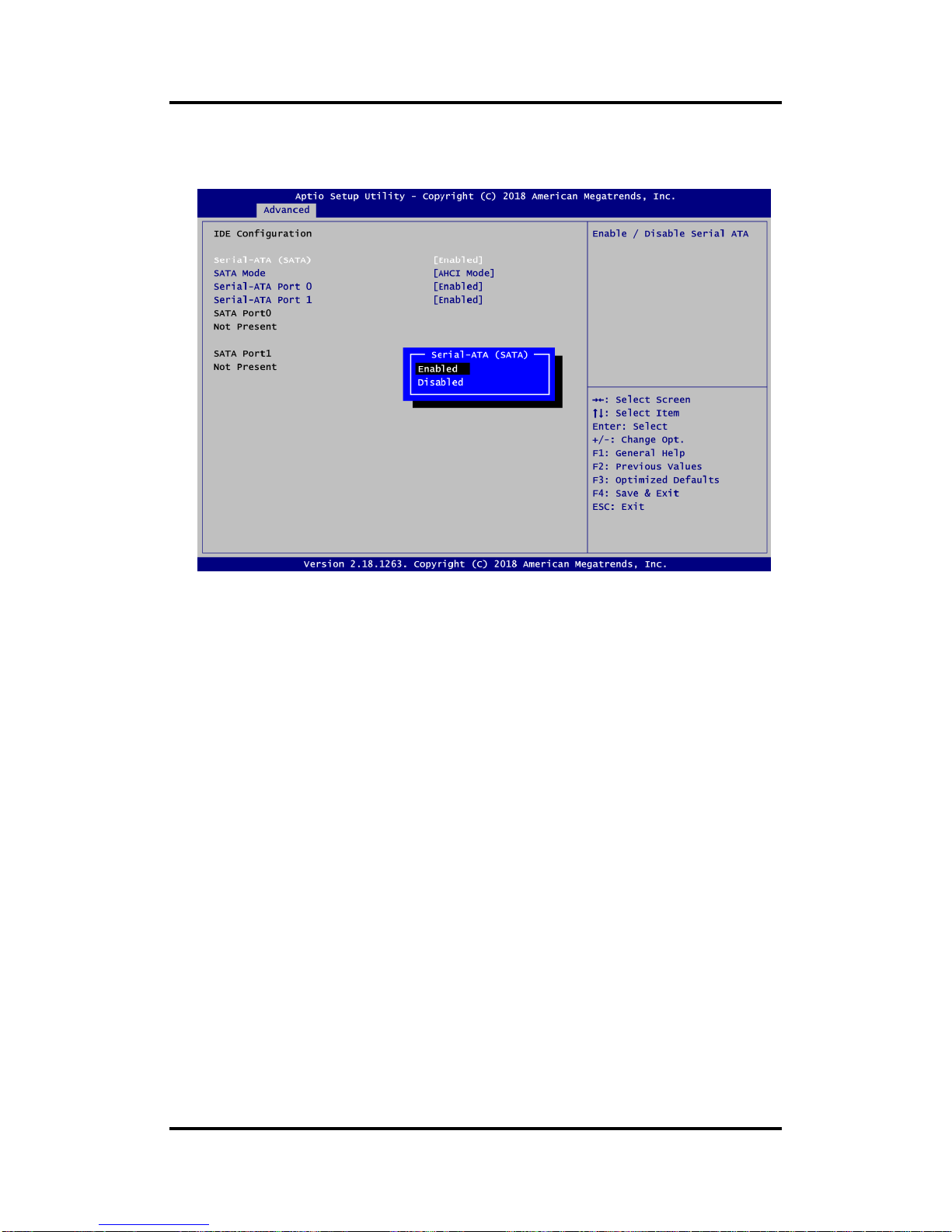
IDE Configuration
In IDE Configuration menu, you can see the current installed hardware in SATA ports.
During system boot up, BIOS automatically detects the presence of SATA devices.
Serial-ATA (SATA)
Enable or disable Chipset SATA Controller.
SATA Mode
Determine how SATA controller(s) operate. Operation mode options are IDE Mode and
AHCI (Advanced Host Controller Interface) Mode.
Serial-ATA Port 0~1
Enable or disable SATA port 0~1
Page 50

CAPA84R Capa Board
44 AMI BIOS Setup Utility
Miscellaneous Configuration
OS Selection
Use this option to do OS selection. The default is Windows
®
10.
If the Window® 7 is needed to be installed via USB 3.0 port (CN19, see section 2.4.17), it is
suggested to select Windows® 7. After installation of Windows® 7, XHCI driver is needed to
be installed to activate USB 3.0 port (CN19, see section 2.4.17).
Note
If the Windows® 10 is selected but install Windows® 7 via USB 3.0 port
(CN19, see section 2.4.17), the fail message may be occurred in installation.
Page 51

CAPA84R Capa Board
AMI BIOS Setup Utility 45
USB Configuration
USB Devices
Display all detected USB devices.
Legacy USB Support
Enable legacy support for USB devices. Auto option disables legacy support if no USB
devices are connected. Disable option will keep USB devices available only for EFI
applications.
Page 52

CAPA84R Capa Board
46 AMI BIOS Setup Utility
Utility Configuration
BIOS Flash Utility
BIOS flash utility configuration. For more detailed information, please refer to Appendix C.
Page 53

CAPA84R Capa Board
AMI BIOS Setup Utility 47
4.5 Chipset Menu
The Chipset menu allows users to change the advanced chipset settings. You can select any
of the items in the left frame of the screen to go to the sub menus:
► North Bridge
► South Bridge
For items marked with “”, please press <Enter> for more options.
Page 54

CAPA84R Capa Board
48 AMI BIOS Setup Utility
North Bridge
This screen allows users to configure parameters of North Bridge chipset.
LVDS Panel Type
Select the appropriate LVDS panel resolution, see image below.
Memory Information
Display system memory information.
Page 55
CAPA84R Capa Board
AMI BIOS Setup Utility 49
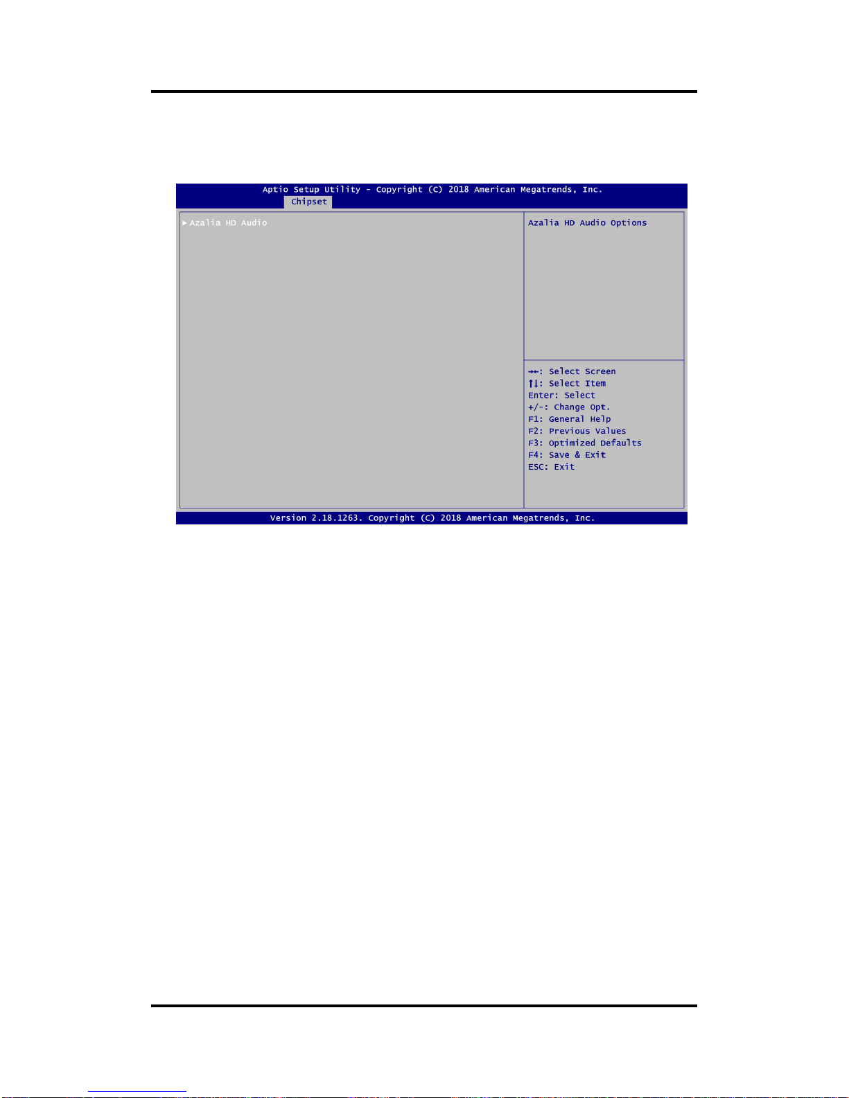
South Bridge
This screen shows the information of South Bridge chipset. A description of the selected
item appears on the right side of the screen. For items marked with “”, please press
<Enter> for more options.
Azalia HD Audio
Use these items to set parameters related to HD Audio configuration. Please press
<Enter> to go to the sub menus.
Page 56

CAPA84R Capa Board
50 AMI BIOS Setup Utility
Audio Controller
Control detection of HD Audio device.
- Disabled: Azalia will be unconditionally disabled.
- Enabled: Azalia will be unconditionally enabled.
Page 57

CAPA84R Capa Board
AMI BIOS Setup Utility 51
4.6 Security Menu
The Security menu allows users to change the security settings for the system.
Administrator Password.
Set administrator password.
User Password
Set user password.
HDD Security Configuration
HDD Security Configuration for selected drive.
Page 58

CAPA84R Capa Board
52 AMI BIOS Setup Utility
4.7 Boot Menu
The Boot menu allows users to change boot options of the system.
Setup Prompt Timeout
Number of seconds to wait for setup activation key. 65535(0xFFFF) means indefinite
waiting.
Bootup NumLock State
Use this item to select the power-on state for the keyboard NumLock.
Quiet Boot
Select to display either POST output messages or a splash screen during boot-up.
PXE ROM
Enable or disable the Preboot eXecution Environment (PXE) boot ROM function of the
onboard LAN chip during system boots up.
Boot Option Priorities [Boot Option #1, …]
These are settings for boot priority. Specify the boot device priority sequence from the
available devices.
Hard Drive BBS Priorities
Set the order of hard drive boot. This option appears only if at least one device of this
group is detected.
Page 59
CAPA84R Capa Board
AMI BIOS Setup Utility 53
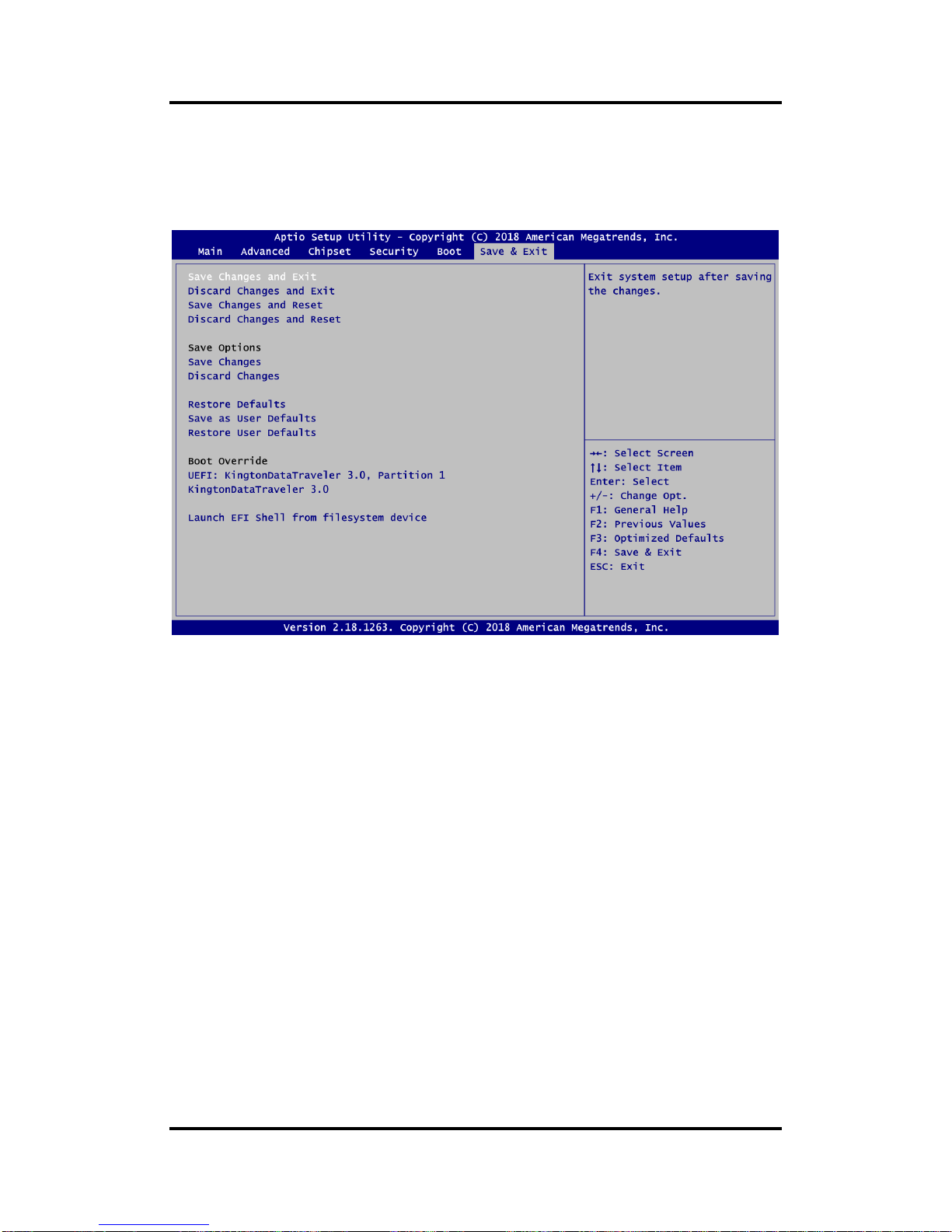
4.8 Save & Exit Menu
The Save & Exit menu allows users to load your system configuration with optimal or fail-safe
default values.
Save Changes and Exit
When you have completed the system configuration changes, select this option to leave
Setup and return to Main Menu. Select Save Changes and Exit from the Save & Exit menu
and press <Enter>. Select Yes to save changes and exit.
Discard Changes and Exit
Select this option to quit Setup without making any permanent changes to the system
configuration and return to Main Menu. Select Discard Changes and Exit from the Save &
Exit menu and press <Enter>. Select Yes to discard changes and exit.
Save Changes and Reset
When you have completed the system configuration changes, select this option to leave
Setup and reboot the computer so the new system configuration parameters can take
effect. Select Save Changes and Reset from the Save & Exit menu and press <Enter>.
Select Yes to save changes and reset.
Discard Changes and Reset
Select this option to quit Setup without making any permanent changes to the system
configuration and reboot the computer. Select Discard Changes and Reset from the Save
& Exit menu and press <Enter>. Select Yes to discard changes and reset.
Save Changes
When you have completed the system configuration changes, select this option to save
changes. Select Save Changes from the Save & Exit menu and press <Enter>. Select Yes
to save changes.
Page 60

CAPA84R Capa Board
54 AMI BIOS Setup Utility
Discard Changes
Select this option to quit Setup without making any permanent changes to the system
configuration. Select Discard Changes from the Save & Exit menu and press <Enter>.
Select Yes to discard changes.
Restore Defaults
It automatically sets all Setup options to a complete set of default settings when you select
this option. Select Restore Defaults from the Save & Exit menu and press <Enter>.
Save as User Defaults
Select this option to save system configuration changes done so far as User Defaults.
Select Save as User Defaults from the Save & Exit menu and press <Enter>.
Restore User Defaults
It automatically sets all Setup options to a complete set of User Defaults when you select
this option. Select Restore User Defaults from the Save & Exit menu and press <Enter>.
Boot Override
Select a drive to immediately boot that device regardless of the current boot order.
Launch EFI Shell from filesystem device
Attempt to launch EFI Shell application (Shellx64.efi) from one of the available filesystem
devices.
Page 61

CAPA84R Capa Board
Watchdog Timer 55
Appendix A
Watchdog Timer
A.1 About Watchdog Timer
Software stability is major issue in most application. Some embedded systems are not
watched by operator for 24 hours. It is usually too slow to wait for someone to reboot when
computer hangs. The systems need to be able to reset automatically when things go wrong.
The watchdog timer gives us solution.
The watchdog timer is a counter that triggers a system reset when it counts down to zero from
a preset value. The software starts counter with an initial value and must reset it periodically. If
the counter ever reaches zero which means the software has crashed, the system will reboot.
A.2 How to Use Watchdog Timer
The I/O port base addresses of watchdog timer are 2E (hex) and 2F (hex). The 2E (hex) and
2F (hex) are address and data port respectively.
Assume that program A is put in a loop that must execute at least once every 10ms. Initialize
watchdog timer with a value bigger than 10ms. If the software has no problems; watchdog
timer will never expire because software will always restart the counter before it reaches zero.
Begin
Enable and Initialize
Watchdog Timer
Program “A”
Disable Watchdog
Timer
Next
Next
Next
Next
Begin
Enable and Initialize
Watchdog Timer
Program “A”
Reset Watchdog
Timer
Next
Next
Next
Next
Page 62

CAPA84R Capa Board
56 Watchdog Timer
A.3 Sample Program
Assembly sample code :
;Enable WDT:
mov dx,2Eh
mov al,87 ;Un-lock super I/O
out dx,al
out dx,al
;Select Logic device:
mov dx,2Eh
mov al,07h
out dx,al
mov dx,2Fh
mov al,07h
out dx,al
;Enable WDT base address:
mov dx,2Eh
mov al,30h
out dx,al
mov dx,2Fh
mov al,01h
out dx,al
;Activate WDT:
mov dx,2Eh
mov al,0F0h
out dx,al
mov dx,2Fh
mov al,80h
out dx,al
;Set base timer :
mov dx,2Eh
mov al,0F6h
out dx,al
mov dx,2Fh
mov al,Mh ;M=00h,01h,...FFh (hex),Value=0 to 255
out dx,al ;(see
Note
below)
;Set Second or Minute :
mov dx,2Eh
mov al,0F5h
out dx,al
mov dx,2Fh
mov al,Nh ;N=71h or 79h(see
Note
below)
out dx,al
Note:
If N=71h, the time base is set to second.
M = time value
00: Time-out disable
01: Time-out occurs after 1 second
02: Time-out occurs after 2 seconds
03: Time-out occurs after 3 seconds
.
.
FFh: Time-out occurs after 255 seconds
Page 63

CAPA84R Capa Board
Watchdog Timer 57
If N=79h, the time base is set to minute.
M = time value
00: Time-out disable
01: Time-out occurs after 1 minute
02: Time-out occurs after 2 minutes
03: Time-out occurs after 3 minutes
.
.
FFh: Time-out occurs after 255 minutes
Page 64

CAPA84R Capa Board
58 Watchdog Timer
This page is intentionally left blank.
Page 65
CAPA84R Capa Board
Digital I/O 59
Appendix B
Digital I/O
B.1 About Digital I/O
The onboard GPIO or digital I/O has 8 bits. Each bit can be set to function as input or output by
software programming. In default, all pins are pulled high with +5V level (according to main
power). The BIOS default settings are 4 inputs and 4 outputs.
CN2
B.2 Digital I/O Programming
I
2
C to GPIO PCA9554PW GPIO.
I
2
C address: 01001000.
Command byte
Command
Protocol
Function
0
Read byte
Input port register
1
Read/write byte
Output port register
2
Read/write byte
Polarity inversion register
3
Read/write byte
Configuration register
The command byte is the first byte to follow the address byte during a write transmission. It is
used as a pointer to determine which of the following registers will be written or read.
Pin
Signal
Pin
Signal
1
DIO0 2 DIO7
3
DIO1 4 DIO6
5
DIO2 6 DIO5 7 DIO3 8 DIO4 9 +5V
10
GND
Page 66
CAPA84R Capa Board
60 Digital I/O
Register 0: Input port register.
This register is a read-only port. It reflects the incoming logic levels of the pins, regardless of
whether the pin is defined as an input or an output by Register 3. Writes to this register have
no effect.
The default “X” is determined by the externally applied logic level, normally “1” when no
external signal externally applied because of the internal pull-up resistors.
Register 0 – Input port register bit description
Bit
Symbol
Access
Value
Description
7
I7
Read only
X
Determined by externally applied
logic level.
6
I6
Read only
X 5 I5
Read only
X 4 I4
Read only
X 3 I3
Read only
X 2 I2
Read only
X 1 I1
Read only
X 0 I0
Read only
X
Register 1: Output port register.
This register reflects the outgoing logic levels of the pins defined as outputs by Register 3. Bit
values in this register have no effect on pins defined as inputs. Reads from this register return
the value that is in the flip-flop controlling the output selection, not the actual pin value.
Register 1 – Output port register bit description
Bit
Symbol
Access
Default Value
Description
7
O7 R 1
Reflects outgoing logic levels of pins defined as
outputs by Register 3.
6
O6 R 1 5 O5 R 1 4 O4 R 1 3 O3 R 1 2 O2 R 1 1 O1 R 1 0 O0 R 1
Register 2: Polarity Inversion register.
This register allows the user to invert the polarity of the Input port register data. If a bit in this
register is set (written with “1”), the corresponding Input port data is inverted. If a bit in this
register is cleared (written with “0”), the Input port data polarity is retained.
Register 2 – Polarity inversion register bit description
Bit
Symbol
Access
Default Value
Description
7
N7
R/W
0
Inverts polarity of Input port register data.
0 = Input port register data retained (default
value).
1 = Input port register data inverted.
6
N6
R/W 0 5
N5
R/W 0 4
N4
R/W 0 3
N3
R/W
0
2
N2
R/W
0
1
N1
R/W 0 0
N0
R/W
0
Page 67
CAPA84R Capa Board
Digital I/O 61
Register 3: Configuration register.
This register configures the directions of the I/O pins. If a bit in this register is set, the
corresponding port pin is enabled as an input with high-impedance output driver. If a bit in this
register is cleared, the corresponding port pin is enabled as an output. At reset, the I/Os are
configured as inputs with a weak pull-up to VDD.
Register 3 – Configuration register bit description
Bit
Symbol
Access
Default Value
Description
7
C7
R/W
1
Configures the directions of the I/O pins.
0 = Corresponding port pin enabled as an output.
1 = Corresponding port pin configured as input
(default value).
6
C6
R/W
1
5
C5
R/W 1 4
C4
R/W 1 3
C3
R/W 1 2
C2
R/W 1 1
C1
R/W 1 0
C0
R/W
1
Page 68

CAPA84R Capa Board
62 Digital I/O
This page is intentionally left blank.
Page 69

CAPA84R Capa Board
BIOS Flash Utility 63
Appendix C
BIOS Flash Utility
The BIOS Flash utility is a new helpful function in BIOS setup program. With this function you
can easily update system BIOS without having to enter operating system. In this appendix you
may learn how to do it in just a few steps. Please read and follow the instructions below
carefully.
1. In your USB flash drive, create a new folder and name it “Axiomtek”, see figure below.
2. Copy BIOS ROM file (e.g. CAPA84R.005) to “Axiomtek” folder.
3. Insert the USB flash drive to your system.
4. Enter BIOS setup menu and go to Advanced\Utility Configuration. Select BIOS Flash
Utility and press <Enter>.
CAPA84R.005
Page 70

CAPA84R Capa Board
64 BIOS Flash Utility
5. BIOS automatically detect all USB drive(s) attached to the system. In this example only
one USB drive is attached to the system. That’s why, you can see only one device is
displayed in figure below.
6. Select the USB drive containing BIOS ROM file you want to update using the <> or
<> key. Then press <Enter> to get into “Axiomtek” folder.
7. Now you can see the BIOS ROM file on the screen, press <Enter> to select.
8. Select Start to flash system BIOS option to begin updating procedure.
CAPA84R.005
Page 71

CAPA84R Capa Board
BIOS Flash Utility 65
9. Please wait while BIOS completes the entire flash update process: erase data, write new
data and verify data.
10. When you see the following figure, press <Enter> to finish the update process. After that
the system will shut down and restart immediately.
 Loading...