D O C - 0 509- 0 1 0 , R E V B
DEMO9S12XHY256
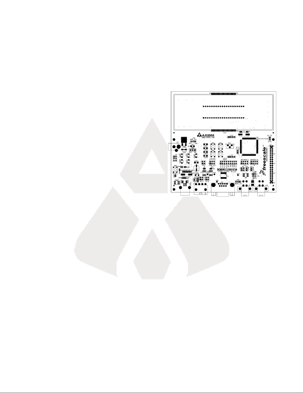
Demonstration Board for Freescale MC9S12XHY256
Microcontroller
USER GUIDE
Web Site: www.axman.com
Support: support@axman.com

D E M O 9 S 1 2 X H Y 2 5 6 J U L Y 1 5 , 2 0 1 0
U S E R G U I D E
CONTENTS
CAUTIONARY NOTES .............................................................................................................. 4
TERMINOLOGY ......................................................................................................................... 4
FEATURES ................................................................................................................................ 5
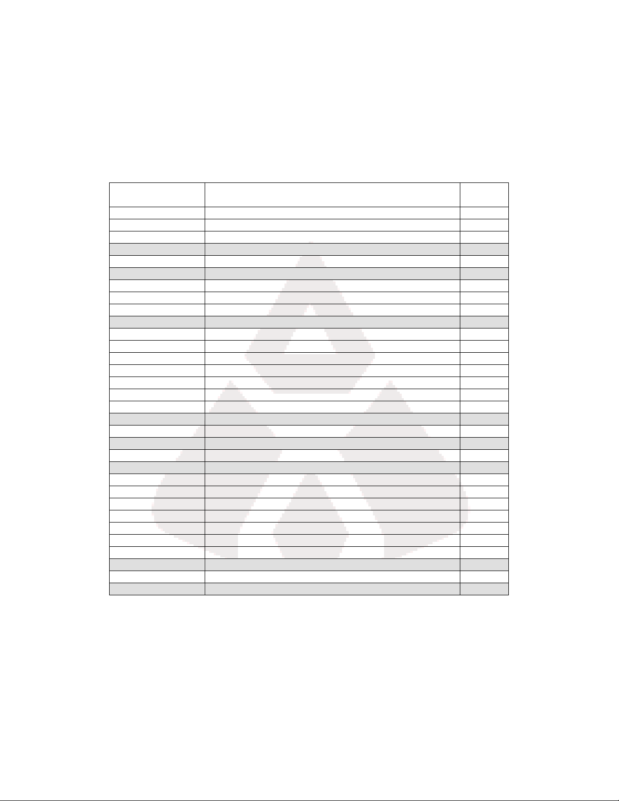
MEMORY MAP .......................................................................................................................... 6
SOFTWARE DEVELOPMENT ................................................................................................... 6
DEVELOPMENT SUPPORT ...................................................................................................... 7
INTEGRATED BDM .............................................................................................................. 7
BDM_PORT HEADER ........................................................................................................... 7
POWER ...................................................................................................................................... 8
POWER SELECT .................................................................................................................. 8
PWR_SEL ......................................................................................................................... 8
VX_EN ............................................................................................................................... 9
RESET SWITCH ...................................................................................................................... 10
LOW VOLTAGE RESET .......................................................................................................... 10
CLOCK ..................................................................................................................................... 10
COMMUNICATIONS ................................................................................................................ 10
RS-232 ................................................................................................................................ 11
COM CONNECTOR ........................................................................................................ 11
COM_SEL ....................................................................................................................... 11
USB SERIAL LINK .............................................................................................................. 12
LIN PORT ............................................................................................................................ 12
LIN ENABLE .................................................................................................................... 13
LIN COM INPUT .............................................................................................................. 13
WAKE OPTION ............................................................................................................... 13
LIN_PWR OPTION .......................................................................................................... 13
MSTR OPTION................................................................................................................ 14
LIN CONNECTOR ........................................................................................................... 14
CAN PORT .......................................................................................................................... 14
CAN TERMINATION ENABLE ................................ ........................................................ 15
STANDBY MODE ............................................................................................................ 16
LCD .......................................................................................................................................... 16
LCD CONNECTIONS .......................................................................................................... 16
MOTOR CONTROLLER .......................................................................................................... 18
MC POWER INPUT ............................................................................................................. 18
MC PWM OUTPUT ............................................................................................................. 18
MCU I/O PORT ......................................................................................................................... 19
USER I/O .................................................................................................................................. 20
2

D E M O 9 S 1 2 X H Y 2 5 6 J U L Y 1 5 , 2 0 1 0
Date
Rev
Comments
June 29, 2010
A
Initial Release
July 15, 2010
B
Minor corrections, Added option reference designators, Re-ordered
document structure, Added acronyms section
U S E R G U I D E
POTENTIOMETER .............................................................................................................. 20
LED’S .................................................................................................................................. 20
PUSHBUTTON SWITCHES ................................................................................................ 20
ACRONYMS ............................................................................................................................. 21
FIGURES
Figure 1: Memory Map................................................................................................................ 6
Figure 2: BDM_PORT Header .................................................................................................... 8
Figure 3: V_SEL Option Header ................................................................................................. 9
Figure 4: VX_EN Option Header .............................................................................................. 10
Figure 5: Serial Connections .................................................................................................... 11
Figure 6: COM1 Connector ....................................................................................................... 11
Figure 7: COM_SEL Option Header ......................................................................................... 12
Figure 8: BCOM_EN Option Header ........................................................................................ 12
Figure 9: LIN Block Diagram ..................................................................................................... 12
Figure 10: Option Header ......................................................................................................... 13
Figure 11: LIN Option Header .................................................................................................. 14
Figure 12: LIN Connector ......................................................................................................... 14
Figure 13: CAN_PORT ............................................................................................................. 15
Figure 14: CAN Termination Enable ......................................................................................... 15
Figure 15: LCD Connections .................................................................................................... 17
Figure 16: Motor Power Input ................................................................................................... 18
Figure 17: Motor Controller I/O PORT ...................................................................................... 19
Figure 18: MCU I/O PORT ........................................................................................................ 19
Figure 19: User Option Header ................................................................................................. 20
REVISION
3

D E M O 9 S 1 2 X H Y 2 5 6 J U L Y 1 5 , 2 0 1 0
U S E R G U I D E
CAUTIONARY NOTES
1) Electrostatic Discharge (ESD) prevention measures should be used when handling this
product. ESD damage is not a warranty repair item.
2) Axiom Manufacturing does not assume any liability arising out of the application or use of
any product or circuit described herein; neither does it convey any license under patent
rights or the rights of others.
3) EMC Information on the DEMO9S12XHY256 board:
a) This product as shipped from the factory with associated power supplies and cables,
has been verified to meet with requirements of CE and the FCC as a CLASS A product.
b) This product is designed and intended for use as a development platform for hardware
or software in an educational or professional laboratory.
c) In a domestic environment, this product may cause radio interference in which case the
user may be required to take adequate prevention measures.
d) Attaching additional wiring to this product or modifying the products operation from the
factory default as shipped may effect its performance and cause interference with
nearby electronic equipment. If such interference is detected, suitable mitigating
measures should be taken.
TERMINOLOGY
This development module utilizes option select jumpers to configure default board operation.
Terminology for application of the option jumpers is as follows:
Jumper – a plastic shunt that connects 2 terminals electrically
Jumper on, in, or installed = jumper is a plastic shunt that fits across 2 pins and the shunt is
installed so that the 2 pins are connected with the shunt.
Jumper off, out, or idle = jumper or shunt is installed so that only 1 pin holds the shunt, no 2
pins are connected, or jumper is removed. It is recommended that the jumpers be placed
idle by installing on 1 pin so they will not be lost.
Cut-Trace – a circuit trace connection between component pads. The circuit trace may be
cut using a knife to break the default connection. To reconnect the circuit, simply install a
suitably sized 0-ohm resistor or attach a wire across the pads.
Signal names followed by an asterisk (*) denote active-low signals.
4

D E M O 9 S 1 2 X H Y 2 5 6 J U L Y 1 5 , 2 0 1 0
U S E R G U I D E
FEATURES
The DEMO9S12XHY256 is a demonstration board for the MC9S12XHY256 microcontroller.
Application development is quick and easy with the integrated USB-BDM, sample software
tools, and examples. An optional BDM_PORT port is also provided to allow use of a
BDM_PORT cable. A 40-pin connector provides access to most IO signals on the target MCU.
MC9S12XHY256, 100 LQFP
S12XCPU
256K Bytes Flash
8K Bytes Data Flash
12K Bytes RAM
8Ch, 12b ADC
Integrated LCD Driver
Integrated 4-Ch Stepper Motor Controller
Integrated Stepper Motor Stall Detect
40MHz Maximum Bus Frequency
On-Board 4x40 Custom LCD Glass
2 ea. High-Speed CAN Physical Layer Transceivers
Enhanced LIN Physical Layer Transceiver
RS-232 Serial Data Physical Layer Transceiver
Integrated USB-BDM
BDM_PORT header for external BDM cable support
MCU_PORT pin header for access to MCU IO signals
On-board +5V regulator
Optional Power from USB-BDM or MCU_PORT connector
Power Input Selection Jumpers
Power input from USB-BDM
Power input from on-board regulator
Power input from Connector J1
Optional Power output through Connector J1
User Components Provided
5 Push Switches; 4 User, 1 Reset
6 LED Indicators; 4 User, +5V, USB
5K ohm POT w /LP Filter
User Option Jumpers to disconnect Peripherals
Connectors
40-pin MCU I/O Pin Header
2.0mm Barrel Connector
BDM_PORT Connector for External BDM Cable
USB Connector
DB9 Connector
4.2mm, 1x4 Molex CAN Cable Connector
4.2mm, 2x2 Molex LIN Cable Connector
Specifications:
Board Size 5.5” x 5.25”
5

D E M O 9 S 1 2 X H Y 2 5 6 J U L Y 1 5 , 2 0 1 0
Address
Module
Size
(Bytes)
0x0000–0x0009
PIM (port integration module)
10
0x000A–0x000B
MMC (memory map control)
2
0x000C–0x000D
PIM (port integration module)
2
0x000E–0x000F
Reserved
2
0x0010–0x0017
MMC (memory map control)
8
0x0018–0x0019
Reserved
2
0x001A–0x001B
Device ID register
2
0x001C–0x001F
PIM (port integration module)
4
0x0020–0x002F
DBG (debug module)
16
0x0030–0x0033
Reserved
4
0x0034–0x003F
ECRG (clock and reset generator)
12
0x0040–0x006F
TIM0 (timer module)
48
0x0070–0x009F
ATD (analog-to-digital converter 10 bit 8-channel)
48
0x00A0–0x00C7
PWM (pulse-width modulator 8 channels)
40
0x00C8–0x00 D7
SCI[1:0] (serial communications interface)
16
0x00D8–0x00DF
SPI (serial peripheral interface)
8
0x00E0–0x00E7
IIC (Inter IC bus)
8
0x00E8–0x00FF
Reserved
24
0x0100–0x0113
FTMR control registers
20
0x0114–0x011F
Reserved
12
0x0120-0x012F
INT (interrupt module)
1
0x0130–0x013F
Reserved
31
0x0140–0x017F
CAN0
64
0x0180–0x01BF
CAN1
64
0x01C0–0x01FF
MC(motor controller)
64
0x0200–0x021F
LCD
32
0x0220–0x023F
Stepper Stall Detector 0 (SSD[3:0])
32
0x0240–0x029F
PIM (port integration module)
96
0x02A0–0x02CF
TIM1(timer module)
48
0x02D0–0x02EF
Reserved
32
0x02F0–0x02F7
Voltage Regulator
8
0x02F8–0x07FF
Reserved
1288
U S E R G U I D E
MEMORY MAP
Figure 1 below shows the device register memory map. Refer to the MC9S12XHY256
Reference Manual (RM) for further information.
Figure 1: Memory Map
SOFTWARE DEVELOPMENT
Software development requires the use of a compiler or an assembler supporting the
HCS12(X) instruction set and a host PC operating a debug interface. CodeWarrior
Development Studio is supplied with this board for application development and debug. Refer
to the supporting CodeWarrior documentation for details on use and capabilities.
6

D E M O 9 S 1 2 X H Y 2 5 6 J U L Y 1 5 , 2 0 1 0
CAUTION:
When powered from the USB bus, do not exceed the 500mA maximum
allowable current drain. Damage to the target board or host PC may
result
NOTE:
10K ohm pull-ups are applied to BDM signals RESET* and BKGD
inside the P&E BDM block. These pull-ups are not shown on the
schematic.
U S E R G U I D E
DEVELOPMENT SUPPORT
Application development and debug for the target MC9S12XHY256 is supported through the
background debug mode (BDM) interface. The BDM interface consists of an integrated USBMultilink BDM and a 6-pin interface header (BDM_PORT). The BDM_PORT header allows
connecting an external HCS12 BDM cable. Refer to the MC9S12XHY Reference Manual for
details and capabilities of the BDM.
Integrated BDM
The DEMO9S12XHY256 board features an integrated USB-BDM. The integrated BDM
supports application development and debug via background debug mode. All necessary
signals are provided by the integrated BDM. A USB, type B, connector provides connection
from the target board to a host PC.
The integrated USB-Multilink BDM provides power and ground to the target board eliminating
the need for external power. Power from the USB-Multilink BDM is derived from the USB bus;
therefore, total current consumption for the target board, and connected circuitry, must not
exceed 500mA. This current limit describes the current supplied by the USB cable to the
BDM circuit, the target board, and any connected circuitry. Excessive current drain will violate
the USB specification causing the bus to disconnect. Damage to the host PC USB hub or the
target board may result.
BDM_PORT Header
An HCS(X)12 compatible BDM cable may be attached to the 6-pin BDM interface header (J2)
if desired. Figure 2 below shows the pin-out for the BDM_PORT header.
7
 Loading...