

Page 1

DOC-0398-010, REV A
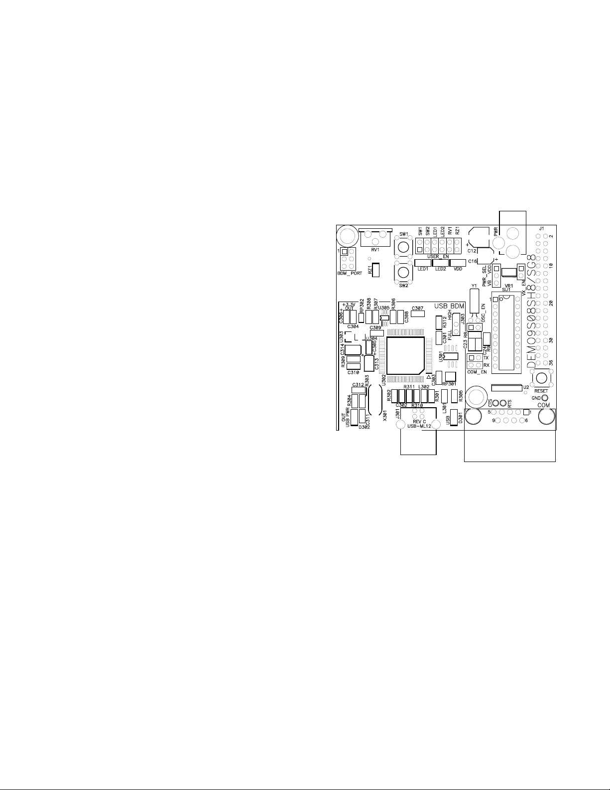
DEMO9S08SH8/SG8
Demonstration Board for Freescale MC9S08SH8/SG8
Axiom Manufacturing • 2813 Industrial Lane • Garland, TX 75041
Email: Sales@axman.com Web: http://www.axman.com
Page 2

DEMO9S08SH8 APRIL 27, 2007
USER GUIDE
CONTENTS
CAUTIONARY NOTES ..............................................................................................................4
TERMINOLOGY.........................................................................................................................4
FEATURES................................................................................................................................5
REFERENCES...........................................................................................................................6
GETTING STARTED..................................................................................................................6
OPERATING MODES................................................................................................................6
RUN MODE........................................................................................................................... 6
DEBUG MODE......................................................................................................................7
MEMORY MAP ..........................................................................................................................7
SOFTWARE DEVELOPMENT...................................................................................................8
DEVELOPMENT SUPPORT......................................................................................................8
INTEGRATED BDM .............................................................................................................. 8
BDM_PORT HEADER........................................................................................................... 9
POWER......................................................................................................................................9
POWER SELECT.................................................................................................................. 9
PWR_SEL.........................................................................................................................9
VX_EN............................................................................................................................. 10
RESET SWITCH ......................................................................................................................11
LOW VOLTAGE RESET..........................................................................................................11
TIMING.....................................................................................................................................11
COMMUNICATIONS................................................................................................................ 11
RS-232 ................................................................................................................................ 12
COM CONNECTOR........................................................................................................ 12
COM_EN......................................................................................................................... 12
USER I/O..................................................................................................................................13
POTENTIOMETER.......................................................................................................... 13
SWITCHES ..................................................................................................................... 13
LED’S.............................................................................................................................. 13
USER SIGNALS.................................................................................................................. 13
USER ENABLE ................................................................................................................... 14
MCU I/O PORT.........................................................................................................................14
2
Page 3

DEMO9S08SH8 APRIL 27, 2007
USER GUIDE
FIGURES
Figure 1: BDM_PORT Header....................................................................................................9
Figure 2: PWR_SEL Option Header.........................................................................................10
Figure 3: VX_EN Option Header ..............................................................................................11
Figure 4: COM Connector.........................................................................................................12
Figure 5: USER Option Header................................................................................................14
Figure 6: MCU I/O PORT – J1..................................................................................................14
TABLES
Table 1: Run Mode Setup...........................................................................................................6
Table 2: BDM Mode Setup .........................................................................................................7
Table 3: Memory Map.................................................................................................................8
Table 4: COM Connections ......................................................................................................12
Table 5: COM_EN Option .........................................................................................................12
Table 6: User I/O...................................................................................................................... 13
REVISION
Date Rev Comments
April 27, 2007 A Initial Release
3
Page 4

DEMO9S08SH8 APRIL 27, 2007
USER GUIDE
CAUTIONARY NOTES
1) Electrostatic Discharge (ESD) prevention measures should be used when handling this
product. ESD damage is not a warranty repair item.
2) Axiom Manufacturing does not assume any liability arising out of the application or use of
any product or circuit described herein; neither does it convey any license under patent
rights or the rights of others.
3) EMC Information on the DEMO9S08SH8 board:
a) This product as shipped from the factory with associated power supplies and cables,
has been verified to meet with requirements of CE and the FCC as a CLASS B product.
b) This product is designed and intended for use as a development platform for hardware
or software in an educational or professional laboratory.
c) In a domestic environment, this product may cause radio interference in which case the
user may be required to take adequate prevention measures.
d) Attaching additional wiring to this product or modifying the products operation from the
factory default as shipped may effect its performance and cause interference with
nearby electronic equipment. If such interference is detected, suitable mitigating measures should be taken.
TERMINOLOGY
This development module utilizes option select jumpers to configure default board operation.
Terminology for application of the option jumpers is as follows:
Jumper – a plastic shunt that connects 2 terminals electrically
Jumper on, in, or installed = jumper is a plastic shunt that fits across 2 pins and the shunt is
installed so that the 2 pins are connected with the shunt.
Jumper off, out, or idle = jumper or shunt is installed so that only 1 pin holds the shunt, no 2
pins are connected, or jumper is removed. It is recommended that the jumpers be placed
idle by installing on 1 pin so they will not be lost.
Cut-Trace – a circuit trace connection between component pads. The circuit trace may be
cut using a knife to break the default connection. To reconnect the circuit, simply install a
suitably sized 0-ohm resistor or attach a wire across the pads.
Signal names followed by an asterisk (*) denote active-low signals.
4
Page 5
DEMO9S08SH8 APRIL 27, 2007
USER GUIDE
FEATURES
The DEMO9S08SH8/SG8 is a demonstration board for the MC9S08SH8 or the MC9S08SG
microcontroller. Application development is quick and easy with the integrated USB-BDM,
sample software tools, and examples. An optional BDM_PORT port is also provided to allow
use of a BDM_PORT cable. Two, 40-pin connectors provide access to all IO signals on the
target MCU.
• MC9S08SH8, 20 PDIP
• 8K Bytes Flash
• 512 Bytes RAM
• Internal Oscillator
• Integrated P&E USB-BDM
• BDM_PORT header for BDM cable support (not installed)
• MCU_PORT socket header for access to MCU IO signals
• On-board +5V regulator
• Optional power from USB-BDM or MCU_PORT connec-
tor
• Power Input Selection Jumpers
• Power input from USB-BDM
• Power input from on-board regulator
• Power input from Connector J1
• Optional Power output through Connector J1
• User Components Provided
• 3 Push Switches; 2 User, 1 Reset
• 7 LED Indicators; 2 User, VDD, USB Power, USB
Power Out
• 5K ohm POTs w /LP Filter
• Light Sensor w/ LP Filter and Op Amp
• Jumpers
• PWR_SEL
• VX_EN
• USER_EN
• COM_EN
• Connectors
• 40-pin MCU I/O Connector
• 2.0mm Barrel Connector
• BDM_PORT (not installed)
• USB Connector
• DB9 Connector
Specifications:
Board Size 2.95 x 2.75”
Power Input: +6VDC to +18VDC
5
Page 6

DEMO9S08SH8 APRIL 27, 2007
USER GUIDE
REFERENCES
Reference documents are provided on the support CD in Acrobat Reader format.
DEMO9S08SH8_UG.pdf DEMO9S08SH8 User Guide (this document)
DEMO9S08SH8_QSG.pdf DEMO9S08SH8 Quick Start Guide
DEMO9S08SH8 _SCH_A.pdf DEMO9S08SH8 Schematic Rev. A
DEMO9S08SH8_Silk_A.pdf DEMO9S08SH8 Top Silk, Rev A
SH8DEMO.zip Demo Program Source Code
GETTING STARTED
To get started quickly, please refer to the DEMO9S08SH8 Quick Start Guide. This quick start
will illustrate connecting the board to a PC, installing the correct version of CodeWarrior Development Studio, and running a simple LED test program.
OPERATING MODES
The DEMO9S08SH8 board operates in two modes: Run Mode, and Debug Mode. Run Mode
executes the user application from Power-On or Reset. Debug Mode supports application
development and debug. See the related sections below for quickly starting the board in the
desired operation mode.
RUN MODE
Run mode executes the user application when power is applied to the board or the RESET
button is pressed. Use the following settings to configure the DEMO9S08SH8 board for RUN
Mode to get started quickly.
1. Connect auxiliary equipment to board as required by application.
2. Configure the board option jumpers for run mode.
Table 1: Run Mode Setup
PWR_SEL Pin1 – Pin2 (VB)
COM_SEL As Required
VX_EN As Required
USER As Required
LIN_EN As Required
NOTE: See Power section below to configure power input from PWR connecto r or from J1 connector.
3. Apply power to the board.
6
Page 7

DEMO9S08SH8 APRIL 27, 2007
USER GUIDE
4. The programmed application will begin to execute.
Debug Mode
Debug Mode supports application development and debug. Debug mode is available to the
user through the integrated USB-Multilink BDM or through the use of an external
HCS12/HCS08 BDM cable. Use of the integrated USB-Multilink BDM requires only a host PC
with an available USB port and an A/B type USB cable. A 6-pin BDM interface header
(BDM_PORT) supports the use of an external HCS08/HCS12 BDM cable. The BDM_PORT
header is not installed in default configuration. The steps below describe using the integrated
USB-Multilink BDM.
1. Connect auxiliary equipment to board as required by application.
2. Install and launch CodeWarrior Development Studio, or P&E PKGHCS08Z tool set.
3. Configure the board option jumpers for DEBUG mode.
Table 2: BDM Mode Setup
PWR_SEL Pin1 – Pin2 (VB)
COM_SEL As Required
VX_EN As Required
USER As Required
LIN_EN As Required
NOTE: Refer to the Development Support section below for details on using an external HCS12 BDM cable.
4. Connect the supplied USB cable between an available USB port on the host PC and the
USB connector on the board.
5. Hosting development software will establish DEBUG communication.
6. Refer to BDM cable documentation for details on use of BDM.
MEMORY MAP
The table below shows the default memory map for the MC9S08SH8 immediately out of reset.
Refer to the MC9S08SH8 Data Sheet (DS) for further information.
7
Page 8

DEMO9S08SH8 APRIL 27, 2007
USER GUIDE
Table 3: Memory Map
$0000 $007F
$0080 $027F
$0280 $17FF
$1800 $185F
$1860 $7FFF
$E000 $FFFF
Direct Page
REGISTERS
RAM 512 bytes
Unimplemented 5504 bytes
High Page Registers 95 bytes
Unimplemented 51104 bytes
FLASH 8192 bytes
128 bytes
SOFTWARE DEVELOPMENT
Software development requires the use of a compiler or an assembler supporting the HCS08
instruction set and a host PC operating a debug interface. CodeWarrior Development Studio
and Axiom IDE for Windows for Debugging and Flash programming are supplied with this
board.
DEVELOPMENT SUPPORT
Application development and debug for the target MC9S08SH8 is supported through a background debug mode (BDM) interface. The BDM interface consists of an integrated USBMultilink BDM and a 6-pin interface header (BDM_PORT). The BDM_PORT header allows
connecting a HCS12/HCS08 BDM cable.
Integrated BDM
The DEMO9S08SH8 board features an integrated USB-Multilink BDM from P&E Microcomputer Systems. The integrated USB-Multilink BDM supports application development and debugging via background debug mode. All necessary signals are provided by the integrated
USB-Multilink BDM. A USB, type B, connector provides connection from the target board to
the host PC.
The integrated USB-Multilink BDM provides +5V power and ground to target board eliminating
the need to power the board externally. Power from the USB-Multilink BDM is derived from the
USB bus; therefore, total current consumption for the target board, and connected circuitry,
must not exceed 500mA. This current limit describes the current supplied by the USB cable
to the BDM circuit, the target board, and any connected circuitry. Excessive current drain will
violate the USB specification causing the bus to disconnect. Damage to the host PC USB hub
or the target board may result.
8
Page 9

DEMO9S08SH8 APRIL 27, 2007
USER GUIDE
BDM_PORT Header
A compatible HCS12 BDM cable can also attach to the 6-pin BDM interface header
(BDM_PORT). This header is not installed in default configuration. The figure below shows
the pin-out for the DEBUG header. This information is included for completeness.
Figure 1: BDM_PORT Header
BKGD
NOTE: This header is not installed in default configuration.
1 2
3 4
5 6
GND
RESET*
VDD
See the MC9S08SH8 Data Sheet for complete
DEBUG documentation
POWER
The DEMO9S08SH8 is designed to allow the user to power the board through the USBMultilink BDM during application development. A 2.0-mm barrel connector has been applied to
support stand-alone operation and to support LIN functionality. The board may also be powered through connector J1. This connection may also be used to supply power from the board
to external circuitry. Optionally, the board may be powered from the LIN connectors.
During application development, the board may be powered from either the USB-BDM or the
PWR connector. To utilize LIN functionality, the board must be powered from PWR connector
with a typical input voltage of +12VDC or from the LIN bus.
POWER SELECT
Power may be applied to the board through the integrated USB-Multilink BDM circuitry, a
2.0mm barrel connector, or through connector J1. Power selection is achieved using 2 selec-
tion headers: PWR_SEL option header and the VX_EN option header.
PWR_SEL
The PWR_SEL option header selects power input either from the integrated USB-Multilink
BDM circuitry or from the on-board voltage regulator. The figure below details the PWR_SEL
header connections.
9
Page 10

DEMO9S08SH8 APRIL 27, 2007
USER GUIDE
Figure 2: PWR_SEL Option Header
VB
1 2 3
PWR_SEL
VB
1 2 3
PWR_SEL
NOTE: Set PWR_SEL jumper to VB during application development. Use barrel connector in-
put (PWR) to support LIN functionality if needed.
VDD
Selects power input from USB-BDM
VDD
Selects power input from on-board regulator or J1
Power from the integrated BDM is drawn from the USB bus and is limited to 500 mA. This current limit accounts for the total current supplied over the USB cable to the BDM circuit, the target board, and any connected circuitry. Current drain in excess of 500 mA will violate the USB
specification and will cause the USB bus to disconnect. This will cause the board to exhibit
power cycling where the board appears to turn-on then off continually. Damage to the host PC
or the target board may also result.
The on-board voltage regulator (VR1) accepts power input through a 2.0mm barrel connector
(PWR). Input voltage may range from +6V to +18V. The voltage regulator (VR1) provides a
+5V fixed output limited to 250mA. Over-temperature and over-current limit built into the voltage regulator provides protection from excessive stress. The user should consider the maximum output current limit of VR1 when attempting to power off-board circuitry through connector J1.
If powered from the PWR connector, the integrated BDM may still be used to develop and debug application code. Alternately, the board may be powered from the integrated BDM while
the LIN bus is powered from the PWR connector.
VX_EN
The VX_EN option header is a 2-pin jumper that connects or disconnects input J1-1 directly to
the target board, +5V voltage rail. J1-3 is directly connected to the ground plane. Use of this
feature requires a regulated +5V input power source. This power input is decoupled to minimize noise but is not regulated. Care should be exercised when using this feature; no protection is applied on this input and damage to the target board may result if over-driven. Also, do
not attempt to power the target board through this connector while also applying power through
the USB-Multilink BDM or the PWR connector; damage to the board may result.
Power may also be sourced to off-board circuitry through the J1 connector. The current supplied from the USB bus or the on-board regulator limits current available to external circuitry.
Excessive current drain may damage the target board, the host PC USB hub, or the on-board
regulator. The figure below details the VX_EN header connections.
10
Page 11

DEMO9S08SH8 APRIL 27, 2007
USER GUIDE
Figure 3: VX_EN Option Header
ON OFF
1 2
VX_EN
CAUTION: Do not exceed available current supply from USB-Multilink BDM or on-board regu-
Enabled Disabled
lator, when sourcing power through connector J1 to external circuitry.
RESET SWITCH
The RESET switch applies an asynchronous RESET to the MCU. The RESET switch is connected directly to the RESET* input on the MCU. Pressing the RESET switch applies a low
voltage level to the RESET* input. A pull-up bias resistor allows normal MCU operation.
Shunt capacitance ensures an adequate input pulse width.
LOW VOLTAGE RESET
The MC9S08SH8 utilizes an internal Low Voltage Detect (LVD) circuit. The LVD holds the
MCU in reset until applied voltage reaches an appropriate level. The LVD also protect against
under-voltage conditions. Consult the MC9S08SH8 reference manual for details LVD operation.
TIMING
The DEMO9S08SH8 is configured to use the target MCU’s internal clock source by default.
Space is provided for an external, 32 kHz XTAL oscillator; however, this timing source is not
populated. The internal timing source is active out of RESET. Default configuration sets the
internal bus to run at 8.4MHz. The internal clock source is trimmable to ± 0.2%. Refer to the
MC9S08SH8 Data Sheet for further details.
COMMUNICATIONS
The DEMO9S08SH8 board applies a single Serial Communications Interface (SCI) port configurable between either SCI or LIN functionality. RS-232 communications are supported
through a DB9 connector. LIN communications are supported through associated pins at connector J1. An option header at COM_EN allows the user to isolate the RS-232 transceiver
from the MCU. This allows the associated MCU pins to be used for alternate functionality.
11
Page 12

DEMO9S08SH8 APRIL 27, 2007
USER GUIDE
RS-232
An RS-232 translator provides RS-232 to TTL/CMOS logic level translation on the COM connector. The COM connector is a 9-pin Dsub, right-angle connector. A ferrite bead on shield
ground provides conducted immunity protection. Communication signals TXD1 and RXD1 are
routed from the transceiver to the MCU. Hardware flow control signals RTS and CTS are
available on the logic side of the transceiver. These signals are routed to vias located near the
transceiver. RTS has been biased properly to support 2-wire RS-232 communications.
Table 4: COM Connections
MCU Port COM Signal I/O PORT
CONNECTOR
PTB1/PIB1/SLTXD/TXD/ADP5 TXD J1-5
PTB0/PIB0/SLRXD/RXD/ADP4 RXD J1-7
COM Connector
A standard 9-pin Dsub connector provides external connections for the SCI0 port. The Dsub
shell is connected to board ground through a ferrite bead. The ferrite bead provides noise
isolation on the RS-232 connection. The figure below details the DB9 connector.
Figure 4: COM Connector
4, 6
TXD
RXD
1, 6
GND
1
2
3
4
5
1, 4
6
RTS
7
CTS
8
NC
9
Female DB9 connector that interfaces to the MCU internal SCI0 serial
port via the RS232 transceiver. Flow control is provided at test points on
the board.
Pins 1, 4, and 6 are connected together.
COM_EN
The RS-232 PHY is connected to the MCU through the COM_EN option header. Installing
shunts in position TX and RX connects the transceiver. Removing the shunts isolates the
transceiver from the MCU.
Table 5: COM_EN Option
ON OFF
1 2
COM_EN
TX Enabled Disabled
RX Enabled Disabled
12
Page 13

DEMO9S08SH8 APRIL 27, 2007
USER GUIDE
USER I/O
User I/O includes 1 potentiometers, 1 Light Sensor, 2 push button switches, and 2 green LEDs
for user I/O. The User option header block enables or disables each User I/O function individually.
Potentiometer
The DEMO9S08SH8 target board provides a 5K ohm potentiometer (POT) to simulate analog
input. The POT is decoupled to minimize noise during adjustment. Potentiometer RV1 connects to analog input PTA0. The figure below shows the USER enable position and associated signal for the potentiometer.
Switches
The DEMO9S08SH8 provides 2 push button switches for user input. Each push button switch
provides an active low input with a pull-up resistor bias to prevent indeterminate input conditions. Pressing a push-button switch causes a low logic input on the associated input. The figure below shows the USER enable position and associated signal for each user switch.
LED’s
The DEMO9S08SH8 target board provides 2 green LEDs for output indication. Each LED is
an active low output. Writing a low logic level to an LED output causes the associated LED to
turn on. A series, current-limit resistor prevents excessive diode current. The figure below
shows the USER enable position and associated signal for each user LED.
User Signals
The following table shows the connections for each user I/O device.
Table 6: User I/O
USER Ref Des Signal Device
1
2
3
4
5
6
SW1 PTA2/PIA2/SDA/ADP2 Push Button Switch
SW2 PTA3/PIA3/SCL/ADP3 Push Button Switch
LED1 PTB6/SDA/XTAL Green LED
LED2 PTB7/SCL/EXTAL Green LED
RV1 PTA0/PIA0/ACMP1+ Potentiometer
RZ1 PTA1/PIA1/ACMP1- Sensor
13
Page 14

DEMO9S08SH8 APRIL 27, 2007
USER GUIDE
User Enable
The User option header block enables or disables each User I/O device individually. User I/O
includes 4 green LEDs, 2 push button switches, one 4-position DIP switch, a Light Sensor, and
a potentiometer. Installing a shunt enables the associated option. Removing a shunt disables
the associated option. The table below shows the configuration option for each USER I/O.
Figure 5: USER Option Header
Shunt
USER Installed Removed Description
1 2
3 4
5 6
7 8
9 10
11 12
SW1 Enable Disable Push Button Switch
SW2 Enable Disable Push Button Switch
LED1 Enable Disable Green LED
LED2 Enable Disable Green LED
RV1 Enable Disable Potentiometer
RZ1 Enable Disable Sensor
MCU I/O PORT
The MCU I/O PORT connector (J1) provide access to the MC9S08SH8 I/O signals. The figures below show the pin-out of the connector J1.
Figure 6: MCU I/O PORT – J1
J1
VDD
VSS
PTB1/PIB1/TXD/ADP5
PTB0/PIB0/RXD/ADP4
PTA2/PIA2/SDA/ADP2
PTA3/PIA3/SCL/ADP3
PTA5/IRQ/TCLK/RESET*
PTA0/PIA0/TPM1CH0/ADP0/AXMP+
PTB3/PIB3/MOSI/ADP7
PTB4/TMP2CH1/MISO
PTB2/PIB2/SPSCK/ADP6
PTB5/TPM1CH1/SS*
PTA1/PIA1/TPC2CH0/ADP1/ACMP-
PTB6/SDA/XTAL
PTC0/TPM1CH0/ADP8
PTC1/TPM1CH1/ADP9
PTC2/ADP10
PTC3/ADP1
12
34
56
78
910
11 12
13 14
15 16
17 18
19 20
21 22
23 24
25 26
27 28
29 30
31 32
33 34
35 36
PTA5/IRQ/TCLK/RESET*
PTA5/IRQ/TCLK/RESET*
PTA4/ACMP0/BKGD/MS
PTB7/SCL/EXTAL
PTB6/SDA/XTAL
NC
NC
NC
PTA1/PIA1/TPC2CH0/ADP1/ACMPPTA0/PIA0/TPM1CH0/ADP0/AXMP+
NC
NC
NC
NC
NC
NC
NC
NC
14
 Loading...