

Page 1

D O C - 0479- 0 1 0 , R E V A
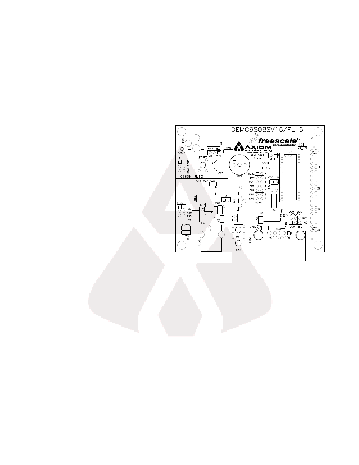
DEMO9S08SV16/FL16
Demonstration Board for Freescale MC9S08SV16 or
MC9S08FL16 Microcontroller
USER GUIDE
Web Site: www.axman.com
Support: support@axman.com
Page 2

D E M O 9 S 0 8 S V 1 6 / F L 1 6 J U N E 5 , 2 0 0 9
U S E R G U I D E
CONTENTS
CAUTIONARY NOTES .............................................................................................................. 4
TERMINOLOGY ......................................................................................................................... 4
FEATURES ................................................................................................................................ 5
REFERENCES ........................................................................................................................... 6
MEMORY MAP .......................................................................................................................... 6
SOFTWARE DEVELOPMENT ................................................................................................... 7
DEVELOPMENT SUPPORT ...................................................................................................... 7
INTEGRATED BDM .............................................................................................................. 7
BDM_PORT HEADER ........................................................................................................... 7
POWER ...................................................................................................................................... 8
POWER SELECT .................................................................................................................. 8
PWR_SEL ......................................................................................................................... 8
VX_EN ............................................................................................................................... 9
RESET SWITCH ...................................................................................................................... 10
LOW VOLTAGE RESET .......................................................................................................... 10
TIMING ..................................................................................................................................... 10
COMMUNICATIONS ................................................................................................................ 10
COM PORT ......................................................................................................................... 10
VIRTUAL COM PORT ......................................................................................................... 11
COM_SEL ........................................................................................................................... 11
COM CONNECTOR ............................................................................................................ 12
USER OPTIONS ...................................................................................................................... 12
PUSHBUTTON SWITCHES ............................................................................................ 12
LED INDICATORS .......................................................................................................... 12
POTENTIOMETER .......................................................................................................... 12
TEMPERATURE SENSOR ............................................................................................. 13
BUZZER .......................................................................................................................... 13
MCU I/O PORT ......................................................................................................................... 14
2
Page 3

D E M O 9 S 0 8 S V 1 6 / F L 1 6 J U N E 5 , 2 0 0 9
Date
Rev
Comments
June 5, 2009
A
Initial Release
U S E R G U I D E
FIGURES
Figure 1: Memory Map................................................................................................................ 6
Figure 2: BDM_PORT Header .................................................................................................... 7
Figure 3: V_SEL Option Header ................................................................................................. 8
Figure 4: VX_EN Option Header ................................................................................................ 9
Figure 5: COM_EN Option Header ........................................................................................... 11
Figure 6: COM Connector ......................................................................................................... 12
Figure 7: MCU I/O PORT – J1 .................................................................................................. 14
TABLES
Table 1: COM Connections ...................................................................................................... 11
Table 2: User Option Jumper Settings ...................................................................................... 13
REVISION
3
Page 4

D E M O 9 S 0 8 S V 1 6 / F L 1 6 J U N E 5 , 2 0 0 9
U S E R G U I D E
CAUTIONARY NOTES
1) Electrostatic Discharge (ESD) prevention measures should be used when handling this
product. ESD damage is not a warranty repair item.
2) Axiom Manufacturing does not assume any liability arising out of the application or use of
any product or circuit described herein; neither does it convey any license under patent
rights or the rights of others.
3) EMC Information on the DEMO9S08SV16/FL16 board:
a) This product as shipped from the factory with associated power supplies and cables,
has been verified to meet with requirements of CE and the FCC as a CLASS A product.
b) This product is designed and intended for use as a development platform for hardware
or software in an educational or professional laboratory.
c) In a domestic environment, this product may cause radio interference in which case the
user may be required to take adequate prevention measures.
d) Attaching additional wiring to this product or modifying the products operation from the
factory default as shipped may effect its performance and cause interference with
nearby electronic equipment. If such interference is detected, suitable mitigating
measures should be taken.
TERMINOLOGY
This development module utilizes option select jumpers to configure default board operation.
Terminology for application of the option jumpers is as follows:
Jumper – a plastic shunt that connects 2 terminals electrically
Jumper on, in, or installed – jumper is a plastic shunt that fits across 2 pins and the shunt is
installed so that the 2 pins are connected with the shunt.
Jumper off, out, or idle – jumper or shunt is installed so that only 1 pin holds the shunt, no 2
pins are connected, or jumper is removed. It is recommended that the jumpers be placed
idle by installing on 1 pin so they will not be lost.
Cut-Trace – a circuit trace connection between component pads. The circuit trace may be
cut using a knife to break the default connection. To reconnect the circuit, simply install a
suitably sized 0-ohm resistor or attach a wire across the pads.
Signal names followed by an asterisk (*) denote active-low signals.
4
Page 5
D E M O 9 S 0 8 S V 1 6 / F L 1 6 J U N E 5 , 2 0 0 9
U S E R G U I D E
FEATURES
The DEMO9S08SV16/FL16 is a demonstration board for the MC9S08SV16 or MC9S08FL16
microcontroller. Application development is quick and easy with the integrated, Open-Source,
USB-BDM, sample software tools, and examples. An optional BDM_PORT port is also
provided to allow use of a BDM_PORT cable. One, 40-pin connector provides access to all IO
signals on the target MCU.
MC9S08SV16 or MC9S08FL16, 32 SDIP
16K Bytes Flash
1K Bytes RAM
RS-232 Serial Data Physical Layer Transceiver
Integrated Open-Source, USB-BDM
BDM_PORT header for external BDM cable
support
MCU_PORT pin header for access to MCU IO
signals
On-board +5V regulator
Optional Power from USB-BDM or MCU_PORT
connector
Power Input Selection Jumpers
Power input from USB-BDM
Power input from on-board regulator
Power input from Connector J1
Optional Power output through Connector
J1
User Components Provided
3 Push Switches; 2 User, 1 Reset
5 LED Indicators; 2 User, VDD, STATUS, TPWR
5K ohm POT w /LP Filter
2300 Hz Piezo Buzzer w/ External Drive Circuit
User Option Jumpers to disconnect Peripherals
Connectors
40-pin MCU I/O Pin Header
2.0mm Barrel Connector
BDM_PORT Connector for External BDM Cable (not installed)
USB Connector
DB9 Connector
Specifications:
Board Size 3.25” x 3.0”
5
Page 6

D E M O 9 S 0 8 S V 1 6 / F L 1 6 J U N E 5 , 2 0 0 9
$0000
$003F
Direct Page Registers
$0040
$043F
RAM
1024 bytes
$0440
$017F
Unimplemented
$1800
$187F
High Page Registers
$1880
$BFFF
Unimplemented
$C000
$DFFF
FLASH
16,384 bytes
U S E R G U I D E
REFERENCES
The following reference documents are available on the CD or DVD provided with this board in
Acrobat Reader format. These documents are also available at www.axman.com/support.
DEMO9S08SV16_FL16_UG.doc DEMO9S08SV16/FL16 User Guide (this document)
DEMO9S08SV16_FL16_SCH_A.pdf DEMO9S08SV16/FL16 Schematic Rev. A
DEMO9S08SV16_FL16_Silk_A.pdf DEMO9S08SV16/FL16 Top Silk, Rev A
DEMO9S08SV16_FL16_Assy_A.pdf DEMO9S08SV16/FL16 Default Shunt Placement
DEMO9S08FL16.zip DEMO9S08FL16 LED Demo Application
DEMO9S08SV16.zip DEMO9S08SV16 LED Demo Application
MEMORY MAP
Figure 1 below shows the default memory map for the MC9S08SV16 and the MC9S08FL16
immediately out of reset. Refer to the MC9S08SV16 or MC9S08FL16 Reference Manual
(RM) for further details.
Figure 1: Memory Map
NOTE: The memory map above applies to the MC9S08SV16 and MC9S08FL16
microcontrollers
6
Page 7

D E M O 9 S 0 8 S V 1 6 / F L 1 6 J U N E 5 , 2 0 0 9
BKGD
1
2
GND
See the MC9S08SV16 or MC9S08FL16 Reference
Manual for details
3
4
RESET*
5
6
VDD
U S E R G U I D E
SOFTWARE DEVELOPMENT
Software development requires the use of a compiler or an assembler supporting the HCS08
instruction set and a host PC operating a debug interface. CodeWarrior Development Studio
for Microcontrollers is supplied with this board for application development and debug. Refer
to the supporting CodeWarrior documentation for details on use and capabilities.
DEVELOPMENT SUPPORT
Application development and debug for the target MC9S08SV16 or MC9S08FL16 is supported
through the integrated, Open-Source Background Debug Mode (BDM) interface. An optional
6-pos BDM_PORT header allows connecting an external HCS12/HCS08 BDM cable. The
BDM_PORT header is not installed in default configurations.
Integrated BDM
The DEMO9S08SV16/FL16 board features an integrated Open Source BDM (OSBDM-JM60)
based on the Freescale MC9S08JM60 MCU. The integrated USB BDM supports application
development and debugging via background debug mode. The integrated BDM is fully
supported by CodeWarrior development tools.
The integrated USB BDM provides power and ground to the target board eliminating the need
to power the board externally. Power from the USB BDM is derived from the USB bus. The
integrated USB BDM is designed to sink a maximum of 300mA of current from the USB bus.
Therefore, total current consumption for the target board, and connected circuitry, must not
exceed 300mA. This current limit describes the current supplied by the USB cable to the
BDM circuit, the target board, and any connected circuitry. Excessive current drain will violate
the USB specification causing the bus to disconnect. Damage to the host PC USB hub or the
target board may result.
BDM_PORT Header
A compatible HCS12 BDM cable may also attach to the 6-pin BDM interface header
(BDM_PORT). Figure 2 below shows the pin-out for the BDM_PORT header.
Figure 2: BDM_PORT Header
NOTE: The BDM_PORT header is not installed in default configuration.
7
Page 8

D E M O 9 S 0 8 S V 1 6 / F L 1 6 J U N E 5 , 2 0 0 9
CAUTION:
Damage to the board may result if voltages greater than +5.5V are applied
at connector J1 input.
PWR_SEL
Enable power to board from integrated BDM
VB VR1
PWR_SEL
Enable power to board from external power supply
VB VR1
U S E R G U I D E
POWER
The DEMO9S08SV16/FL16 may be powered from the integrated USB-BDM or from an onboard voltage regulator and external power connector. The desired power source is selected
using the PWR_SEL option header.
For application development and debug, the board may be powered from the integrated USB
BDM. As noted above, total current consumption from this source is limited to 300 mA. A
2.0mm, center-positive, barrel connector (VIN) and on-board regulator supports stand-alone
operation and higher power requirements.
Power may also be applied to connector J1 or the board may be configured to supply power
from connector J1 to external circuitry.
POWER SELECT
Power may be applied to the board through the integrated BDM circuitry, a 2.0mm barrel
connector, or through connector J1. Power selection is achieved using 2 selection headers:
the PWR_SEL option header and the VX_EN option header.
PWR_SEL
The PWR_SEL option header allows the user to select power input either from either an
external power source connected to the VIN connector or from the integrated USB-BDM.
Figure 3 below details the PWR_SEL header connections.
Figure 3: V_SEL Option Header
8
Page 9

D E M O 9 S 0 8 S V 1 6 / F L 1 6 J U N E 5 , 2 0 0 9
CAUTION:
Do not configure the target board to draw more than 300mA when
powered from the integrated USB BDM. Damage to the target board or
host PC may result otherwise.
ON
OFF
1
2
Enabled
Disabled
VX_EN
CAUTION:
Do not exceed available current from USB-BDM or on-board regulator
when sourcing power through connector J1 to external circuitry.
U S E R G U I D E
Power from the integrated BDM is drawn from the USB bus and is limited to 300 mA. This
current limit accounts for the total current supplied over the USB cable to the BDM circuit, the
target board, and any connected circuitry. Current drain in excess of value violates the USB
specification and will cause the USB bus to disconnect. This will cause the board to exhibit
power cycling where the board appears to turn off and back on continually. Damage to the
host PC or the target board may result.
Although the on-board regulator can accept voltage input to +25VDC, the applied voltage
should not exceed +12V to prevent the regulator (VR1) from overheating.
VX_EN
The VX_EN option header is a 2-pin jumper that connects or disconnects input J1-1 directly to
the target board voltage rail. J1-3 connects directly to the target board ground plane. Use of
this feature requires a regulated input power source. This power input is decoupled to
minimize noise but is not regulated or protected. Care should be exercised when using this
feature; no protection is applied on this input and damage to the target board may result if
excessive voltage is applied. Also, do not attempt to power the target board through this
connector while also applying power through the USB BDM or the PWR connector; damage to
the board may result.
Power may also be sourced to off-board circuitry through the J1 connector. The current
supplied from the USB bus or the on-board regulator limits current available to external
circuitry. Excessive current drain may damage the target board, the host PC USB hub, or the
on-board regulator. The figure below details the VX_EN header connections.
Figure 4: VX_EN Option Header
9
Page 10

D E M O 9 S 0 8 S V 1 6 / F L 1 6 J U N E 5 , 2 0 0 9
U S E R G U I D E
RESET SWITCH
The RESET switch applies an asynchronous RESET to the MCU. The RESET switch is
connected directly to the RESET* input on the MCU. Pressing the RESET switch applies a
low voltage level to the RESET* input. A pull-up bias resistor allows normal MCU operation.
Shunt capacitance ensures an adequate input pulse width.
Both the MC9S08SV16 and MC9S08FL16 MCU’s apply a multiplexed RESET* input. To use
the RESET switch, the RESET pin must be enabled (SOPT1_RSTPE). Refer to the
MC9S08SV16 or MC9S08FL16 Reference Manual for details on configuring using the RESET*
input.
LOW VOLTAGE RESET
Both the MC9S08SV16 and the MC9S08FL16 apply an internal Low Voltage Detect (LVD)
circuitry. The LVD holds the MCU in reset until applied voltage reaches the appropriate level.
The LVD also protects against under-voltage conditions. Consult the MC9S08SV16 or
MC9S08FL16 Reference Manual for details on LVD operation.
TIMING
Default timing for the DEMO9S08SV16/FL16 is provided by the MC9S08SV16 or
MC9S08FL16 internal timing source which is active out of RESET. External circuitry for an
external 32 kHz XTAL oscillator is provided; however, these components are not populated in
default configuration. Refer to the MC9S08SV16 or MC9S08FL16 Reference Manual for
details on configuring the timing source.
COMMUNICATIONS
Serial communication on the DEMO9S08SV16/FL16 board is supported through an RS-232
physical layer interface and DB-9 connector and through a virtual serial port implemented in
the USB-BDM. The COM_SEL option header selects between the applied serial function.
NOTE: Virtual serial port services are not functional as of the date of this document
COM Port
An RS-232 transceiver provides RS-232 to TTL/CMOS logic level translation between the
COM connector and the MCU. The COM connector is a 9-pin Dsub, right-angle connector. A
ferrite bead on shield ground provides conducted immunity protection. Communication signals
TXD and RXD are routed from the transceiver to the MCU. These signals are also available
on connector J1. Hardware flow control signals RTS and CTS are available on the logic side
10
Page 11
D E M O 9 S 0 8 S V 1 6 / F L 1 6 J U N E 5 , 2 0 0 9
MCU Port
COM Signal
I/O PORT
CONNECTOR
PTB1/KBIP5/TXD/ADP5
TXD
J1-5
PTB0/KBIP4/RXD/ADP4
RXD
J1-7
BDM COM
●
Select virtual COM port through USB-BDM
●
COM_SEL
COM BDM
●
Select RS-232 PHY
COM_SEL
U S E R G U I D E
of the RS-232 transceiver and are routed to test point vias located near the transceiver. RTS
has been biased properly to provide handshaking if required.
RS-232 signals TXD and RXD are connected to the MCU through the COM_SEL option
header. Table 1 below shows the RS-232 signal connections.
Table 1: COM Connections
Virtual COM Port
The UART output from the target MCU is connected to the BDM through the COM_SEL
header. Future enhancements to the BDM firmware will support a Virtual COM Port through
the USB-BDM. This functionality is not currently supported.
NOTE: Virtual serial port services are not functional as of the date of this document
COM_SEL
The COM_SEL option header selects between the virtual serial port implemented through the
USB-BDM or the RS-232 PHY. Figure 5 below shows the shunt positions to select between
the two options.
Figure 5: COM_EN Option Header
NOTE: Virtual serial port services are not functional as of the date of this document
11
Page 12

D E M O 9 S 0 8 S V 1 6 / F L 1 6 J U N E 5 , 2 0 0 9
4, 6
1
Female DB9 connector that interfaces to the HC(S)08 internal SCI1 serial
port via the U2 RS232 transceiver. It provides simple 2-wire
asynchronous serial communications without flow control. Flow control is
provided at test points on the board.
Pins 1, 4, and 6 are connected together.
6
1, 4
TXD
2
7
RTS
RXD
3
8
CTS
1, 6
4
9
NC
GND
5
U S E R G U I D E
COM Connector
A standard 9-pin Dsub connector provides external connections for the SCI port. The Dsub
shell is connected to board ground through a ferrite bead. The ferrite bead provides noise
isolation on the RS-232 connection. Figure 6 below, shows the pin-out of the DB9 connector.
Figure 6: COM Connector
USER OPTIONS
The DEMO9S08SV16/FL16 includes various input and output devices to aid application
development and debug. User I/O includes 2 momentary pushbutton switches, 2 green LEDs,
1 potentiometer, 1 temperature sensor, and 1 piezo buzzer. Each device may be enabled or
disabled individually with the USER_EN option header. Each user enable is clearly marked as
to functionality.
Pushbutton Switches
Two push button switches provide momentary, active-low input, for user applications. Pull-ups
internal to the MCU must be enabled to provide error free switch operation. Pushbutton
switches SW1 and SW2 are enabled to the MCU I/O ports by the USER option bank. Table 2
below shows the user jumper settings and MCU connections.
LED Indicators
Two LEDs provide visual output for user applications. Both LEDs are configured for activehigh operation. Table 2 below shows the user jumper settings and MCU connections.
Potentiometer
A 5k ohm, thumb-wheel type, potentiometer at RV1 provides variable resistance input for user
applications. The output is the result of a voltage divider that changes as the thumb-wheel is
turned. The potentiometer is connected between VDD and GND with the center tap providing
the divider output. Table 2 below shows the user jumper settings and MCU connection.
12
Page 13

D E M O 9 S 0 8 S V 1 6 / F L 1 6 J U N E 5 , 2 0 0 9
Jumper
On
Off
MCU PORT
BUZZ
Enable BUZZ
Disable BUZZ
PTB4/TMP1CH0
TEMP
Enable TEMP
Disable TEMP
PTA0/KBIP0/ADP0
POT
Enable POT
Disable POT
PTA1/KBIP1/ADP1
LED1
Enable LED1
Disable LED1
PTB2/KBIP6/ADP6
LED2
Enable LED2
Disable LED2
PTB3/KBIP7/ADP7
SW1
Enable SW1
Disable SW1
PTA2/KBIP2/ADP2
SW2
Enable SW2
Disable SW2
PTA3/KBIP3/ADP3
U S E R G U I D E
Temperature Sensor
A surface-mount, NTC Thermistor (B = 3900) is installed at location RZ1. This component
provides a voltage input to the MCU inversely proportional to temperature. Table 2 below
shows the user jumper settings and MCU connections.
Buzzer
An externally modulated piezo-buzzer, with a center frequency of 2300 Hz for audible
applications is applied. A push-pull drive circuit allows the target MCU to easily drive the
buzzer. Table 2 below shows the user jumper settings and MCU connections.
Table 2: User Option Jumper Settings
NOTE: Signal names in BOLD are not available on the 9S08FL16 derivative
13
Page 14

D E M O 9 S 0 8 S V 1 6 / F L 1 6 J U N E 5 , 2 0 0 9
SV16
FL16
FL16
SV16
VDD
VDD
1 2 PTA5/IRQ*/TCLK/RESET*
PTA5/IRQ*/TCLK/RESET*
VSS
VSS
3 4 PTA5/IRQ*/TCLK/RESET*
PTA5/IRQ*/TCLK/RESET*
PTB1/KBIP5/TxD/ADP5
PTB1/TXD/ADP5
5 6 PTA4/BKGD/MS
PTA4/ACMPO/BKGD/MS
PTB0/KBP4/RxD/ADP4
PTB0/RXD/ADP4
7 8 NC
NC
PTA2/KBIP2/ADP2
PTA2/ADP2
9
10
NC
NC
PTA3/KBIP3/ADP3
PTA3/ADP3
11
12
NC
NC
PTC0/ADP8
PTC0/ADP8
13
14
PTA0/ADP0
PTA0/KBIP0/ADP0
PTC1/ADP9
PTC1/ADP9
15
16
PTA1/ADP1
PTA1/KBIP1/ADP1
PTB3/KBIP7/ADP7
PTB3/ADP7
17
18
NC
NC
PTB4/TPM1CH0
PTB4/TPM1CH0
19
20
NC
NC
PTB2/KBIP6/ADP6
PTB2/ADP6
21
22
PTA6/TMP2CH0
PTA6/TPM2CH0
PTB5/TPM1CH1
PTB5/TPM1CH1
23
24
PTA7/TPM2CH1
PTA7/TPM2CH1
PTD1/SDA
PTD1
25
26
PTB7/EXTAL
PTB7/EXTAL
PTD2/TPM1CH2
PTD2/TPM1CH2
27
28
PTB6/XTAL
PTB6/XTAL
PTD0/SCL
PTD0
29
30
PTD4
PTD4/TPM1CH4
PTD3/TPM1CH3
PTD3/TPM1CH3
31
32
PTD5
PTD5/TPM1CH5
PTC2/ADP10/ACMP+
PTC2/ADP10
33
34
NC
NC
PTC3/ADP11/ACMP
PTC3/ADP11
35
36
NC
NC
PTC4/SS
PTC4
37
38
PTC7
PTC7/MISO
PTC5/SPSCK
PTC5
39
40
PTC6
PTC6/MOSI
U S E R G U I D E
MCU I/O PORT
The MCU I/O PORT connector provides access to the MC9S08SV16 or MC9S08FL16 I/O
signals. Figure 7 below show the pin-out for the MCU I/O connector.
Figure 7: MCU I/O PORT – J1
14
 Loading...