

Axcera 79XITS-7026, 79XITS-7040, 79XITS-7025 User Manual

Transmitter Output Power Amplifier Module Bias Protection
Model Rating Style Board
5721 2.5W QAM
10W Analog 1 Section Bias Protection Board
20W PEP
5722 5W QAM
20W Analog 3 Section Bias Protection Board
40W PEP
5723 10W QAM
30W Analog Feed Forward 3 Section Bias Protection Board
50W PEP Linearization
5724 15W QAM
50W Analog Feed Forward 5 Section Bias Protection Board
70W PEP Linearization
31

Bias Protection Board
The RF power transistors contained in the amplifier module are supplied current and voltage
through the bias protection board. The number of transistors contained in the amplifier
module determines the size of the Bias Protection Boards as listed in the previous table.
Logic circuitry on this board protects the transistors by shutting off power to the module in
the event that the gate bias voltage is lost. This circuitry also monitors the status of the
amplifier module and triggers fault conditions in the Control and Monitoring Module if either
a transistor is damaged or the gate bias voltage is lost.
Dual Power Detector
Detection of the forward and reflected output power levels is performed by the Dual Power
Detector Board. This board produces DC outputs representing the forward and reflected
output power levels of the transmitter. Depending on the type of modulation used in the
system the Power Detector can be configured for either average power detection or peak
power detection by positioning the selection jumper on the back of the board. If the system
is to be used to transmit a QAM signal average detection should be selected. If the system is
to be used to transmit an analog video signal the peak detection should be selected. There
are also a set of potentiometers and test points on the front of the module to provide a
means of calibrating the detection circuitry. There are two zero adjustments and
two metering level adjustments used to calibrate the detector outputs for 1V at 100% power.
When the transmitter is used with an analog video scrambling system that suppresses the
synchronizing pulse there are two additional potentiometers provided to realign the power
detection with these types of video signals. They work with a gating pulse that is applied to
the detector module and is provided by the scramling system. This pulse signals the detec
tor to readjust its gain during the regions of video where the synchronizing pulse has been
suppressed.
Power Amplifier Module Controls
Potentiometers Description
FWD LEV Forward Level Adjust potentiometer calibrates the forward power metering level.
REFL LEV Reflected Level Adjust potentiometer calibrates the reflected power metering level.
FWD ZERO Forward Zero Adjust potentiometer calibrates the zero level for the forward power
metering.
REFL ZERO Reflected Zero Adjust potentiometer calibrates the zero level for the reflected power
metering.
GATE LEV Gate Level Adjust potentiometer sets the detected forward power level in conjunction
with an external gating pulse provided by certain video scrambling systems to properly
reference the peak power level.
GATE TMG Gate Timing Adjust potentiometer sets the trigger timing of an external gating pulse
provided by certain video scrambling systems to properly reference the peak power
level.
32

Test Points Description
FWD DET LEV T/P Forward Power Detection Level Test Point provides a DC voltage that is pro-
portional to the forward output power of the transmitter. (1V=100%)
REFL DET LEV T/P Reflected Power Detection Level Point provides a DC voltage that is propor-
tional to the reflected output power of the transmitter. (1V=100%)
ENV DET T/P Envelope Detection Test Point provides a representation of the RF envelope
used to align the gating pulse provided by certain video scrambling systems to
properly reference the peak power level.
Jumpers
J2 Peak / Average Detection peak 2,3
average 1,2
33
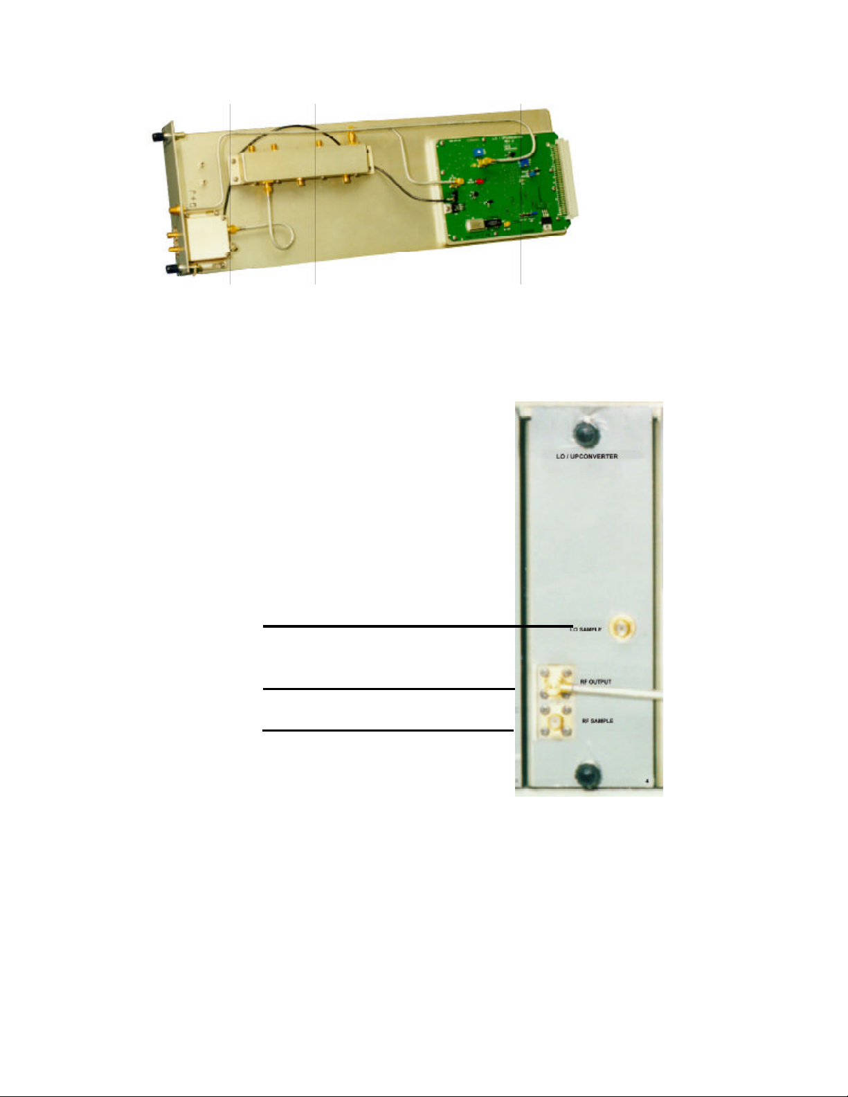
LO / Upconverter Module
LO Sample - SMA connector
RF Output - SMA connector
Sample - SMA connector
34

This module consists of the A1, LO/ Upconverter board, a channel filter, and an output
amplifier board. This module takes an external IF and converts it to the final RF output
frequency using an internally generated local oscillator.
The local oscillator consists of a VCO that is phase locked to an external 10 MHz reference.
The 10 MHz reference and the VCO are both divided down to 500kHz and compared by the
phase lock loop. Error signal from this comparison is generated in the form of an error cur
rent that is converted to a bias voltage to the VCO. This voltage adjusts the output fre
quency of the VCO until it is on the desired frequency.
Phase lock loop is programmed by loading in data generated by the control module . This
data sets the dividers so that the 10MHz and the VCO frequency are divided to 500kHz.
These divide numbers are loaded into U6 using the clock, data and LE lines. This data is
sent whenever the module is first plugged into the back plain or when power is applied to the
tray. This is necessary because the divide numbers are lost when power is removed from the
module.
There is an alarm generated if the phase locked loop is unlocked. This alarm is displayed
locally and is also sent to the control module in the transmitter to be displayed as a fault.
The bias voltage to the VCO is also available to be monitored at TP1 and also can be viewed
an the transmitter front panel display. Normal values for this voltage are 0.5 to 5V.
The 10 MHz reference is normally an external reference. There is also a high stability inter
nal reference option that is available if there is a desire to operate the transmitter without
an external reference. Jumper W1 determines whether an external or internal high stability
reference is to be used.
The IF signal is applied at a level of -5dbm peak sync plus sound and is converted to the
final RF channel frequency. The RF signal is applied to a filter that selects the right conver
sion product. Next, the signal is amplified to -7 dBm by A3 and exits the front of the module
at J2. There is also a front panel sample of the RF output , J3, and the LO, J1. The RF
sample level is approximately -20 dB below the RF output. The LO sample level is -13 dBm.
Jumpers
J2 Internal / external 10 MHz reference internal 2,3
external 1,2
J4 Setup / operate to set L.O. oscillator frequency operate 1,2
works with R10 setup frequency adjustment setup 2,3
35
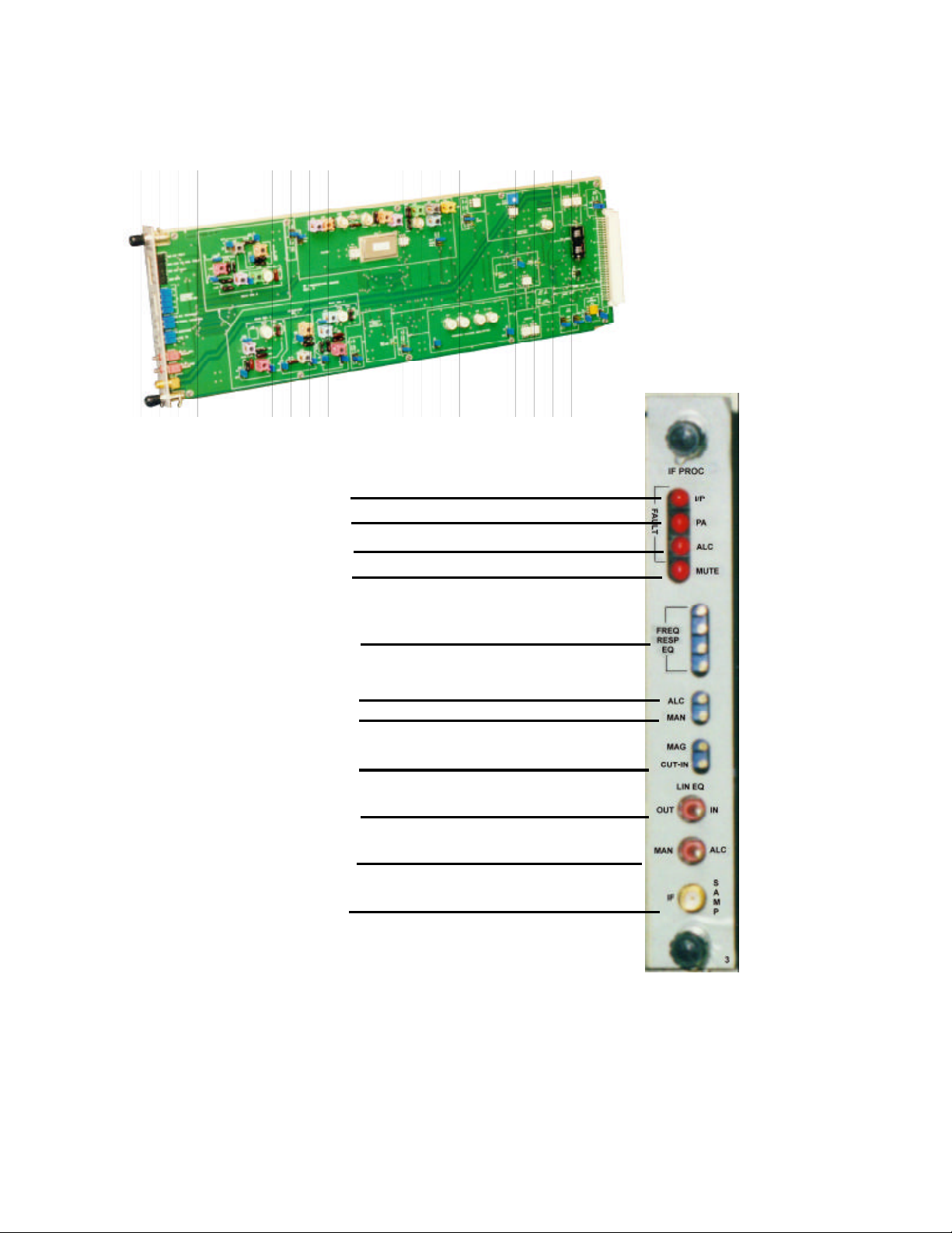
IF Processor Module
The IF Processing module provides frequency response, group delay, and linearity equal
ization for the transmission system. This module also monitors and controls the level of
output power generated by the power amplifier.
I/P - red LED indicates an input fault
P/A - red LED indicates a PA fault (peak to ave)
ALC - red LED indicates an ALC fault
MUTE - red LED indicates loss of video
or IF when in ALC Mode.
Frequency Response Equalization -
ALC -sets reference level of the ALC circuit.
MAN -adjusts gain when ALC is disabled.
MAG/CUT-IN-MAG potentiometer to set linear
equalization of system. CUT-IN sets reference power
level above when the linearity equalization is active.
OUT/IN - Toggle switch that changes linearity
equalization out or in
MAN/ALC -Toggle switch that changes linearity
equalization into ALC or manual
IF SAMPLE - SMA connector
36

The circuitry of the IF Processor Module goes through the following stages as described in
the text that follows.
Impedance Matching and Gain Selection Circuitry
The IF input signal is applied from the backplane connection to J1-32B, the DIN connector
located at the back of the module. An input impedance transformer can be set to 50Ω or
75Ω using jumper J28 and J29. The input range is selected with the I/P gain jumpers J8,
J9, J10, and J11.
Gain Jumper Setting Input Range
HI Gain -22 to -12 dBm PEP
MED Gain -17 to -7 dBm PEP
LO Gain -12 to -2 dBm PEP
37

Input Signal Detection Circuitry
A sample of the IF input signal that is taken through a directional coupler after passing
through the impedance matching and gain circuitry, is applied to an envelope detector. The
average and peak amplitudes of the envelope are measured and sent to a set of comparator
circuits. These circuits will detect the following fault conditions if present.
Fault Condition Action
Input Fault The peak level of the input signal When the module is in ALC mode set the input fault line
drops below the specified I/P range J1-8C to logic low and mute ALC circuitry. Illuminate RED
Peak vs The average level of the input signal is Set the peak vs average line to logic low and mute the ALC
Average Fault 1dB or less below the peak level of the curcuitry. Illuminate RED P/A fault LED.
input signal
The peak vs average fault condition can be enabled or disabled with jumper J30 on the
module
Frequency Response Equalization Circuitry
I/P fault LED
Placing jumper J2 and J3 to the IN position will form a four point frequency response equal
ization circuit in the IF path to offset any frequency response in the system.
Output Signal Detection Circuitry
Analog DC signals relating the level of output power generated by the power amplification
stages of the system provide feedback to the ALC circuit. These signals are applied to the IF
processing module through DIN connectors J1-24C INNER LOOP IN and J1-25C OUTER
LOOP IN. Next, the signals are processed through the output signal detection circuitry before
being applied to the ALC circuit.
The inner loop signal is a DC voltage that originates from within the unit that contains the IF
processing module and represents the level of RF output power generated from the PA stages
of the unit. The optional outer loop signal is a DC voltage generated from outside the unit
and represents the level of RF output power generated from an external amplifier. For both
signals 1 volt equals 100% output power. The output signal detection circuit selects one of
these signals and applies it to the ALC circuit. If the outer loop signal is greater than 90% it
will be selected, otherwise the inner loop signal will be selected. Both signals are buffered
and sent back out of the module through DIN connectors J1-23C and J1-26C. Test point
TP5 loop voltage is used to measure the level of the loop signal being applied to the ALC
circuit.
38

Automatic Level Control Circuitry
A voltage controlled attenuator placed after the frequency response equalization circuit
allows dynamic adjustment of the IF signal gain and provides a means of controlling the
level of output power generated by the power amplification stages of the system.
Mode Operation
Manual - the attenuator gain is controlled manually by The voltage to the attenuator can be adjusted directly by
selecting the manual mode of operation with the toggle the manual gain poteniometer R149 on the front of the module
switch SW2 on the front of the module
ALC - the output power of the system is controlled The desired level of output power can be adjusted from the
automatically by selecting the ALC mode of operation fron of the module by the ALC potentiometer R139. The ALC
with the toggle switch SW2 on the front of the module. circuit will automatically adjust the voltage to the attenuator in
The voltage to the attenuator can be monitored externally through the DIN connection J111C ALC VOLTAGE. If the attenuator voltage exceeds 8V the Red ALC FAULT LED on the
front of the module will illuminate. If this occurs the ALC has reached the end of its operat
ing range and will no longer maintain the proper output power level.
order to maintain the desired output power.
Certain conditions will also place the ALC in a mute state. In this condition the attenuator
voltage is reduced to zero and the level of output is extremely low. A red LED labeled MUTE
on the front of the module indicates this condition. The mute status can also be monitored
externally through DIN connector J1-9 which is set to logic low when the ALC circuit is in a
mute state, however when operating in manual mode the mute condition will be overidden.
Various conditions are described in the table below.
Condition Action
The input signal detection circuitry senses an input fault. The ALC will be forced into the mute state to prevent
transmission of noise.
The input signal detection circuitry senses a peak vs The ALC will be forced into the mute state to prevent
average fault overloading the final transit path and the antenna.
An external device is commanding the ALC circuit to There is an external mute signal that can be applied to the
be placed in the mute state. module through DIN connector J1-10C MUTE I/P. Pulling this
connection to ground will force the ALC circuit to the mute
state.
39

Group Delay Equalization Circuitry
A set group of delay equalizer circuits can be inserted into the signal path after the ALC
attenuator circuit. These have been designed for improved group delay performance for
certain filtering and channel combining schemes. A description of these circuits are given
below.
Equalizer Circuit Operation
Delay Equalizer 1 Selected for equalization of digital systems using adjacent or channel combiners
selected with jumper J35 and J36 non adjacent channel combiners as well as analog systems using adjacent
Attenuation Equalizer 1 Always selected when delay equalizer 1 is selected
selected with jumper J37 and J38
Delay Equalizer 2 Selected for equalization of lumped element band pass filter circuit which
selected with jumper J43 and J44 can also be selected on the module
Delay Equalizer 3 Selected for equalization of analog systems using adjacent or non adjacent
selected with jumper J33 and J34 channel combiners
Equalizer Circuit Operation
Delay Equalizer 1 Selected for analog systems using adjacent combiners
selected with jumper J35 and J36
44 MHz Version
combiners
36 MHz Version
Attenuation Equalizer 1 Always selected when delay equalizer 1 is selected
selected with jumper J37 and J38
Delay Equalizer 2 Selected for equalization of lumped element band pass filter circuit which
selected with jumper J43 and J44 can also be selected on the module
Delay Equalizer 3 Selected for equalization of analog systems using adjacent or non adjacent
selected with jumper J33 and J34 channel combiners
Attenuation Equalizer 3 Always selected when delay equalizer 3 is selected
selected with jumper J33 and J34
Band Pass Filtering Circuitry
Several selections of band pass filters are provided after delay equalization to reduce out of
band products.
Filter Circuit Operation
BPF Used in most analog and digital systems. Delay equalization for this filter
Lumped element band pass filter is activated by selecting delay equalizer 2
SAW (optional) Used in digital systems that require sharper out of band filtering of the
Surface acoustic wave filter IF input
NONE Filtering is bypassed with this option.
40
 Loading...