

Page 1
SERVICE MANUAL
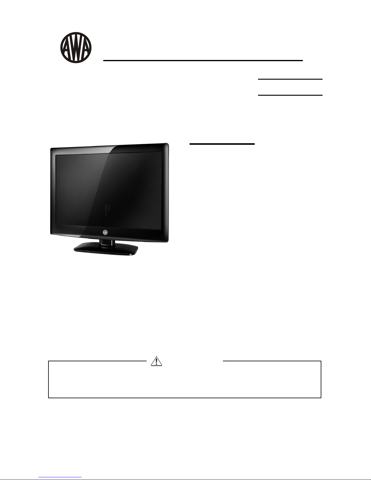
LCD TV
Model No.
MSDV2413-03-D0
Chassis
MSD306
This service information is designed for experienced repair technicians only and is not designed for use by the general public.
It does not contain warnings or cautions to advise non-technical individuals of potential dangers in attempting to service a product.
Products powered by electricity should be serviced or repaired only by experienced professional technicians. Any attempt to
service or repair the product or products dealt with in this service information by anyone else could result in serious injury or death.
WARNING
Page 2

1-1. Table of Contents
1. General Information...........................................................................
1-1. Table of Contents
1-3. Important Notice
1
Chapter 1: General Information
1
3
1-2. General Guidelines
1-4. How to Read this Service Manual
3
6
2. Specifications....................................................................................
Service Manual
Model No.:
- 01 -
3. Location of Controls and Components...........................................
3-1. Board Location
3-2. Main Board & AV Board
3-3. Power Board
3-4. LCD Panel
4. Disassemble and Assemble..........................................................
4-1 Remove the Pedestal
6
88
8
8
11
12
15
15
4-2 Remove the Back Cover 15
4-3 Remove the Adhesive Tape 15
4-4 Remove the Power Module 16
4-5 Remove the Main Board
16
4-6 Remove the Speaker 17
4-7 Remove the Remote Control Board 17
5. Installation Instructions..…....………………...........………….........
18
5-1 External Equipment Connections
18
5-2 HDMI Connections
21
6. Operation Instructions....
…....………………...........………….........
24
6-1 Front Panel Controls
6-2 Back Panel Controls
6-3 Universal Remote Control
24
24
25
7. Electrical Parts…....………………...........………….........................
26
7-1. Block Diagram
8-1. How to enter into the factory model
8-2. How to update software
7-2. Circuit Diagram
7-3. Wiring Connection Diagram
26
27
42
35
43
8. Measurements and Adjustments........…………............................
39
Page 3

Service Manual
Model No.:
- 02 -
9. Trouble-shooting
…………..............................................................
44
9-1. Simple Check 44
9-2. Main Board Failure Check
9-3. Panel Failure
45
52
10. DVD OPERATION
…………..............................................................
57
11.DVD TROUBLE SHOOTING
…………..............................................................
61
Page 4

1-2. General Guidelines
When servicing, observe the original lead dress. If a short circuit is found, replace all parts
which have been overheated or damaged by the short circuit.
After servicing, see to it that all the protective devices such as insulation barriers, insulation
papers shields are properly installed.
After servicing, make the following leakage current checks to prevent the customer from
being exposed to shock hazards.
1) Leakage Current Cold Check
2) Leakage Current Hot Check
3) Prevention of Electro Static Discharge (ESD) to Electrostatically Sensitive
1-3. Important Notice
1-3-1. Follow the regulations and warnings
Most important thing is to list up the potential hazard or risk for the service personnel to
open the units and disassemble the units. For example, we need to describe properly
how to avoid the possibility to get electrical shock from the live power supply or charged
electrical parts (even the power is off).
This symbol indicates that high voltage is present inside.It is dangerous to
make any king of contact with any inside part of this product.
This symbol indicates that there are important operating and maintenance
instructions in the literture accompanying the appliance.
1-3-2. Be careful to the electrical shock
To prevent damage which might result in electric shock or re, do not expose this TV set
to rain or excessive moisture. This TV must not be exposed to dripping or splashing water,
and objects lled with liquid, such as vases, must not be placed on top of or above the TV.
1-3-3. Electro static discharge (ESD)
Some semiconductor (solid state) devices can be damaged easily by static electricity. Such
components commonly are called Electrostatically Sensitive (ES) Devices. The following
techniques should be used to help reduce the incidence of component damage caused by
electros static discharge (ESD).
1-3-4. About lead free solder (PbF)
This product is manufactured using lead-free solder as a part of a movement within the
consumer products industry at large to be environmentally responsible. Lead-free solder
must be used in the servicing and repairing of this product.
1-3-5. Use the genewing parts (specied parts)
Special parts which have purposes of fire retardant (resistors), high-quality sound
(capacitors), low noise (resistors), etc. are used.
When replacing any of components, be sure to use only manufacture's specified parts
shown in the parts list.
Safety Component
● Components identied by mark have special characteristics important for safety.
Service Manual
Model No.:
- 03 -
Page 5

1-3-6 Safety Check after Repairment
- 04 -
Service Manual
Model No.:
Conrm that the screws, parts and wiring which were removed in order to service are put
in the original positions, or whether there are the positions which are deteriorated around
the serviced places serviced or not. Check the insulation between the antenna terminal or
external metal and the AC cord plug blades. And be sure the safety of that.
General Servicing Precautions
1. Always unplug the receiver AC power cord from the AC power source before;
a. Removing or reinstalling any component, circuit board module or any other receiver
assembly.
b. Disconnecting or reconnecting any receiver electrical plug or other electrical
connection.
c. Connecting a test substitute in parallel with an electrolytic capacitor in the receiver.
CAUTION: A wrong part substitution or incorrect polarity installation of electrolytic
capacitors may result in an explosion hazard.
2. Test high voltage only by measuring it with an appropriate high voltage meter or other
voltage measuring device (DVM, FETVOM, etc) equipped with a suitable high voltage
probe.
Do not test high voltage by "drawing an arc".
5. Do not defeat any plug/socket B+ voltage interlocks with which receivers covered by this
service manual might be equipped.
8. Use with this receiver only the test xtures specied in this service manual.
CAUTION: Do not connect the test xture ground strap to any heat sink in this receiver.
3. Do not spray chemicals on or near this receiver or any of its assemblies.
4. Unless specified otherwise in this service manual, clean electrical contacts only by
applying the following mixture to the contacts with a pipe cleaner, cotton-tipped stick or
comparable non-abrasive applicator; 10% (by volume) Acetone and 90% (by volume)
isopropyl alcohol (90%-99% strength).
CAUTION: This is a ammable mixture.
Unless specied otherwise in this service manual, lubrication of contacts is not required.
Capacitors may result in an explosion hazard.
6. Do not apply AC power to this instrument and/or any of its electrical assemblies unless
all solid-state device heat sinks are correctly installed.
7. Always connect the test receiver ground lead to the receiver chassis ground before
connecting the test receiver positive lead.
Always remove the test receiver ground lead last. Capacitors may result in an explosion
hazard.
9. Remove the antenna terminal on TV and turn on the TV.
10. Insulation resistance between the cord plug terminals and the eternal exposure metal
should be more than Mohm by using the 500V insulation resistance meter.
11. If the insulation resistance is less than M ohm, the inspection repair should be required.
If you have not the 500V insulation resistance meter, use a Tester. External exposure
metal: Antenna terminal Headphone jack
Page 6

Service Manual
Model No.:
- 05 -
Electrostatically Sensitive (ES) Devices
1-3-7. Ordering Spare Parts
1. Immediately before handling any semiconductor component or semiconductorequipped assembly, drain off any electrostatic charge on your body by touching a known
earth ground. Alternatively, obtain and wear a commercially available discharging wrist
strap device, which should be removed to prevent potential shock reasons prior to applying
power to the unit under test.
2. After removing an electrical assembly equipped with ES devices, place the assembly
on a conductive surface such as aluminum foil, to prevent electrostatic charge buildup or
exposure of the assembly.
5. Do not use freon-propelled chemicals. These can generate electrical charges sufcient
to damage ES devices.
7. Immediately before removing the protective material from the leads of a replacement
ES device, touch the protective material to the chassis or circuit assembly into which the
device will be installed.
CAUTION: Be sure no power is applied to the chassis or circuit, and observe all other
safety precautions.
3. Use only a grounded-tip soldering iron to solder or unsolder ES devices.
Some semiconductor (solid-state) devices can be damaged easily by static electricity.
Such components commonly are called Electrostatically Sensitive (ES) Devices.
Examples of typical ES devices are integrated circuits and some field-effect transistors
and semiconductor "chip" components. The following techniques should be used to help
reduce the ncidence of component damage caused by static by static electricity.
4. Use only an anti-static type solder removal device. Some solder removal devices not
classied as "anti-static" can generate electrical charges sufcient to damage ES devices.
6. Do not remove a replacement ES device from its protective package until immediately
before you are ready to install it.
(Most replacement ES devices are packaged with leads electrically shorted together by
conductive foam, aluminum foil or comparable conductive material).
8. Minimize bodily motions when handling unpackaged replacement ES devices.
(Otherwise harmless motion such as the brushing together of your clothes fabric or the
lifting of your foot from a carpeted oor can generate static electricity sufcient to damage
an ES device.)
Please include the following informations when you order parts. (Particularly the Version
letter)
1. Model number, Serial number and Software Version
The model number and Serial number can be found on the back of each product and the
Software Version can be found at the Spare Parts List.
2. Spare Part No. and Description
You can nd them in the Spare Parts List
Page 7

- 06 -
Service Manual
Model No.:
1-3-8. Photo used in this manual
The illustration and photos used in this Manual may not base on the final design of
products, which may differ from your products in some way.
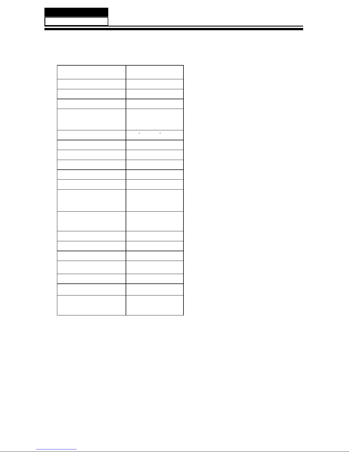
1-4. How to Read this Service Manual
Using Icons:
Icons are used to attract the attention of the reader to specic information. The meaning of
each icon is described in the table below:
Note:
A “note” provides information that is not indispensable, but may nevertheless be valuable
to the reader, such as tips and tricks.
Caution:
A “caution” is used when there is danger that the reader, through incorrect manipulation,
may damage equipment, loose data, get an unexpected result or has to restart(part of) a
procedure.
Warning:
A “warning” is used when there is danger of personal injury.
Reference:
A “reference” guides the reader to other places in this binder or in this manual, where he/
she will nd additional information on a specic topic.
Page 8
Service Manual
Model No.:
- 07 -
2. Specifications
Model
MSDV2413-03-D0
Screen Size 23.6inch
Aspect Ratio
16:9
Resolution
1920*1080
Response Time (ms)
8 (GRAY TO
GRAY)
Angel of View
Color Display
16.7M
No. of Preset Channels 400
OSD Language English
Color System PAL/SECAM
Audio System
DK, BG, I, M, L, L'
Audio Output Power
(Built-in) (W)
3W×2
Audio Output Power
(outer) (W)
No
Total Power Input (W) 60W
Voltage Range (V)
AC100V-240V
Power Frequency (Hz)
50~60Hz
Net Weight (KG)
5.56
Gross Weight (KG)
7.04
Net Dimension (MM)
577*170*427
Packaged Dimension
(MM)
650*201*494
176(H)/176(V)
Page 9
- 08 -
Service Manual
Model No.:
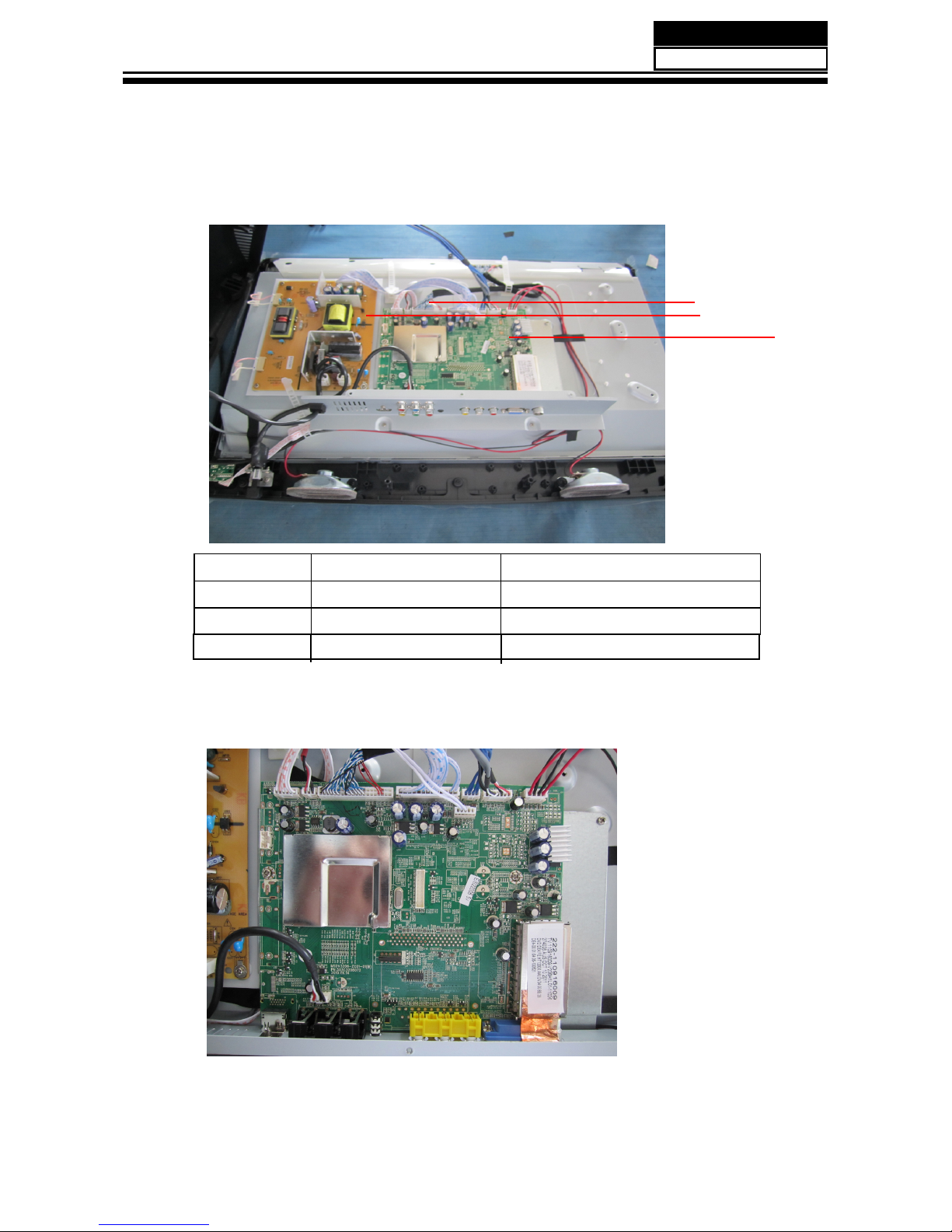
3. Location of Controls and Components
3-1 Board Location
No. Description
A Board Main Board
B Board
Power Board
3-2 Main Board
A Board
B Board
C
C
LVDS WIRE
30433920301
514C2411M14
515C3206M57
Page 10
Service Manual
Model No.:
- 09 -
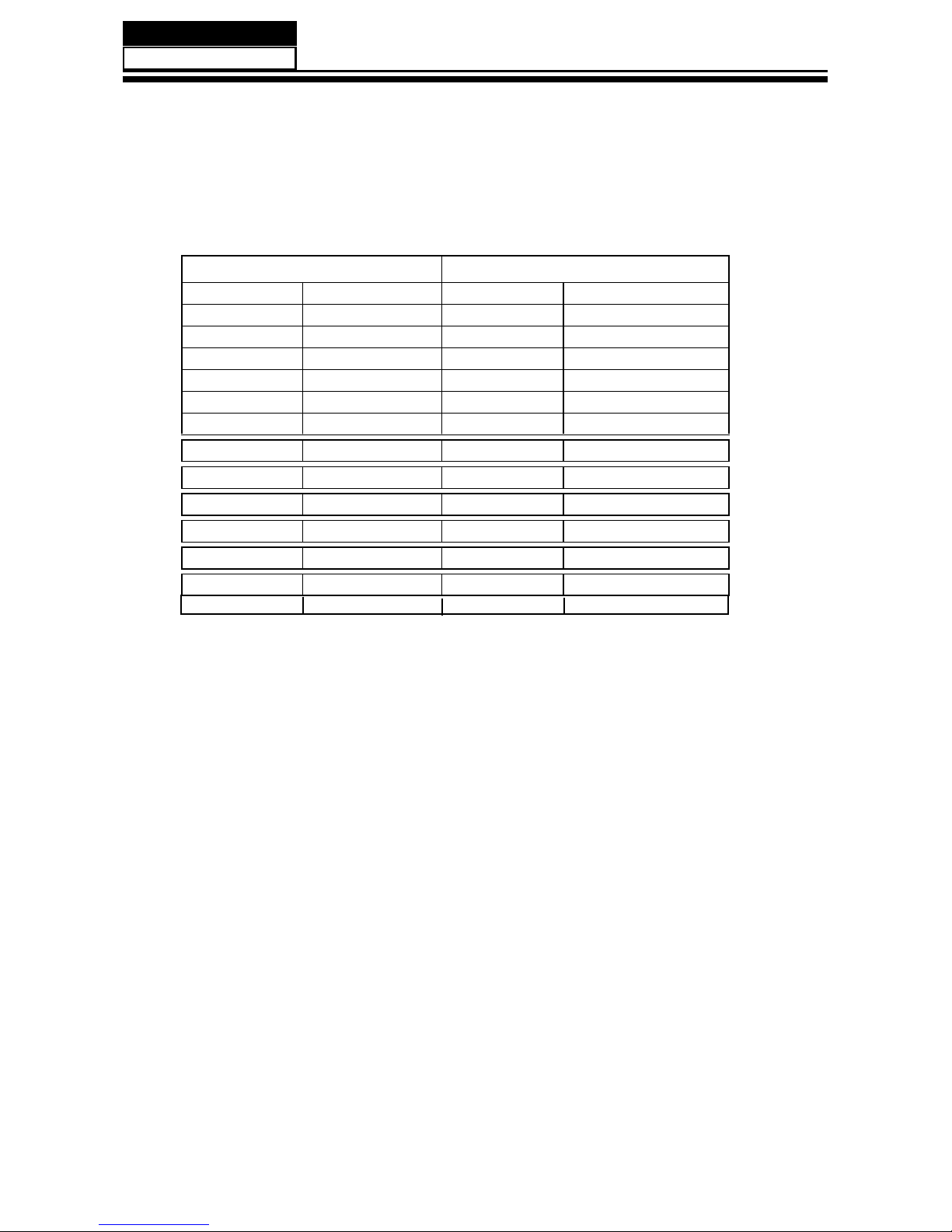
3-2-1 Function Description:
Main Board
Process signal which incept from exterior equipment then translate into signal that panel
can display.
3-2-2 Connector denition
Main board connector
Power connectors (J2,J25)
J2
Pin number Signal name
1 GND
2
ADJ
3 BK ON /OFF
4
+5V
5 POWER ON/OFF
6 +5VSTB
7 +5V
8
+5V
9 GND
10 GND
11 GND
12
+12V
Notes:
J2-Pin 3: Backlight on/off:
The system can turn on or turn off the backlight of TFT LED Panel through the power
supply unit path.
J2-Pin 5: System power on / standby
System board will use this pin to control system power.
J2-Pin 2: Control the luminance of backlight
The system can generate the PWN signal to control the strength of TFT LED Panel’s
backlight through this connector
13 +12V
J25
Pin number
Signal name
1
2
3
4
5
+5V
BL ON/OFF
ADJ
+5V
GND
Page 11
- 10 -
Service Manual
Model No.:
3LQQXPEHU 6LJQDOQDPH 'HVFULSWLRQ
/('B5 /$035('
/('B* /$03*5((1
,5 5(027(&21752/
*1' *1'
9 32:(5)255(027(
3LQQXPEHU 6LJQDOQDPH 'HVFULSWLRQ
.(<
.(<
*1'
remote connector (J21)
Keypad and connector (J22)
Speaker connectorJ26
Pin number Signal name Description
1 RSPK+ RSPK+
2 RSPK- RSPK3 LSPK- LSPK4 LSPK+ LSPK+
Page 12

3-3. Power Board
3-3-1 Function Description:
Supply power for Main board, Panel.
3-3-2Connectordefinition
Service Manual
Model No.:
- 11 -
CON5
Pin number Signal name
Pin number Signal name
9
10
11
12
PWR-ON/OFF
GND
GND
DIM
+12V
BL-ON
GND
GND
+12V
+5V
+5V
5V-STBY
Page 13
3-4. LED Panel
- 12 -
Service Manual
Model No.:
V236H1-L01
Page 14

Service Manual
Model No.:
- 13 -
3-4- Connector defi
nition.
Pin
Name Description
1
RXO0- Negative LVDS differential data input. Channel O0 (odd)
2
RXO0+ Positive LVDS differential data input. Channel O0 (odd)
3
RXO1- Negative LVDS differential data input. Channel O1 (odd)
4
RXO1+ Positive LVDS differential data input. Channel O1 (odd)
5
RXO2- Negative LVDS differential data input. Channel O2 (odd)
6
RXO2+ Positive LVDS differential data input. Channel O2 (odd)
7
GND Ground
8
RXOC- Negative LVDS differential clock input. (odd)
9
RXOC+ Positive LVDS differential clock input. (odd)
10
RXO3- Negative LVDS differential data input. Channel O3(odd)
11
RXO3+ Positive LVDS differential data input. Channel O3 (odd)
12
RXE0- Negative LVDS differential data input. Channel E0 (even)
13
RXE0+ Positive LVDS differential data input. Channel E0 (even)
14
GND Ground
15
RXE1- Negative LVDS differential data input. Channel E1 (even)
16
RXE1+ Positive LVDS differential data input. Channel E1 (even)
17
GND Ground
18
RXE2- Negative LVDS differential data input. Channel E2 (even)
19
RXE2+ Positive LVDS differential data input. Channel E2 (even)
20
RXEC- Negative LVDS differential clock input. (even)
21
RXEC+ Positive LVDS differential clock input. (even)
22
RXE3- Negative LVDS differential data input. Channel E3 (even)
23
RXE3+ Positive LVDS differential data input. Channel E3 (even)
24
GND Ground
25
NC For LCD internal use only, Do not connect
26
NC For LCD internal use only, Do not connect
27
NC For LCD internal use only, Do not connect
28
Vcc +5.0V power supply
29
Vcc +5.0V power supply
30
Vcc +5.0V power supply
Note (1) Connector Part No.: STM MSAKT2407P30HA or Equivalent
Note (2) Mating Wire Cable Connector Part No.: FI-X30H(JAE) or FI-X30HL(JAE)
Note (3) Mating FFC Cable Connector Part No.: 217007-013001 (P-TWO) or JF05X030-1 (JAE)
Note (4) The first pixel is odd.
Note (5) Input signal of even and odd clock should be the same timing.
Page 15

4. Disassemble and assemble
Remove the front frame on the
gure above
① Lay down the unit so that rear cover
faces upward
① Remove the three screw from the
rear cover indicated with ○
① Then remove the pedestal
4-2Remove the Back Cover
① Remove the these screw indicated on
gure above by ○
① Then remove the back cover from the
unit.
Service Manual
Model No.:
- 15 -
4-1 Remove the Pedestal
4-3. Remove the adhesive tape
Page 16
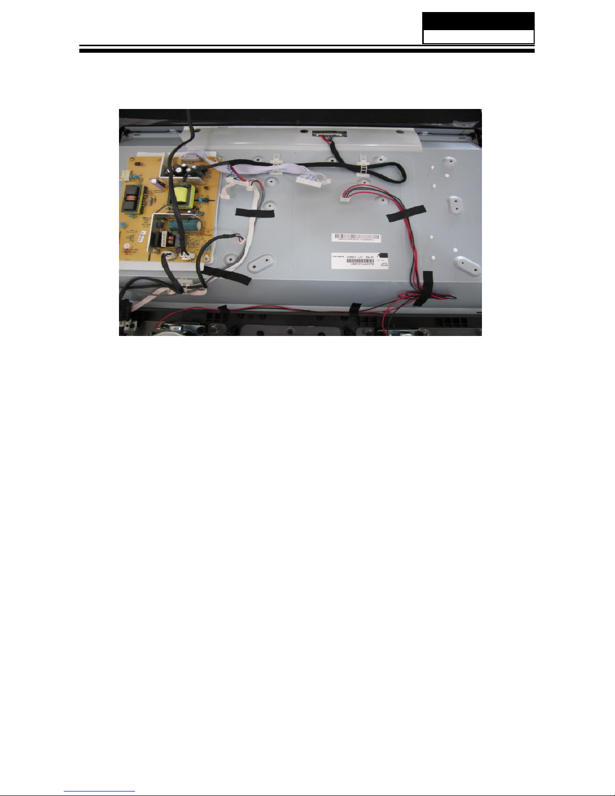
4-4 Remove the main board
① Remove the two screw indicated on
the gure above by ○
①
Then put the terminal bracket to the side
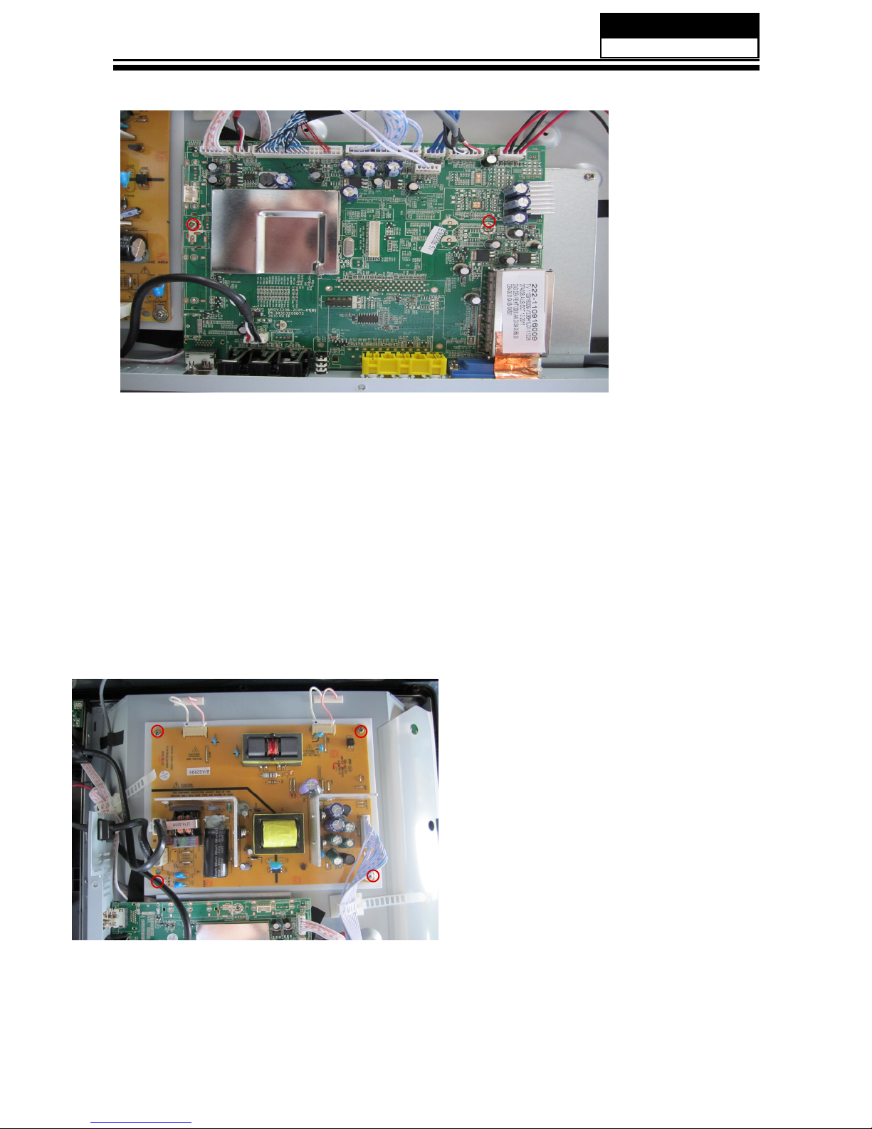
4-5 Remove the power module
① Remove the four screw indicated on the
gure above by ○
①
Then remove the power module
① Disconnected the coupler ① ①
①
①
Remove the Main board
Service Manual
Model No.:
- 16 -
J21 J22 J20 J2 J25
J10 J11 J26 J17
J21 J22 J20 J2 J25
J10 J11 J26 J17
Page 17
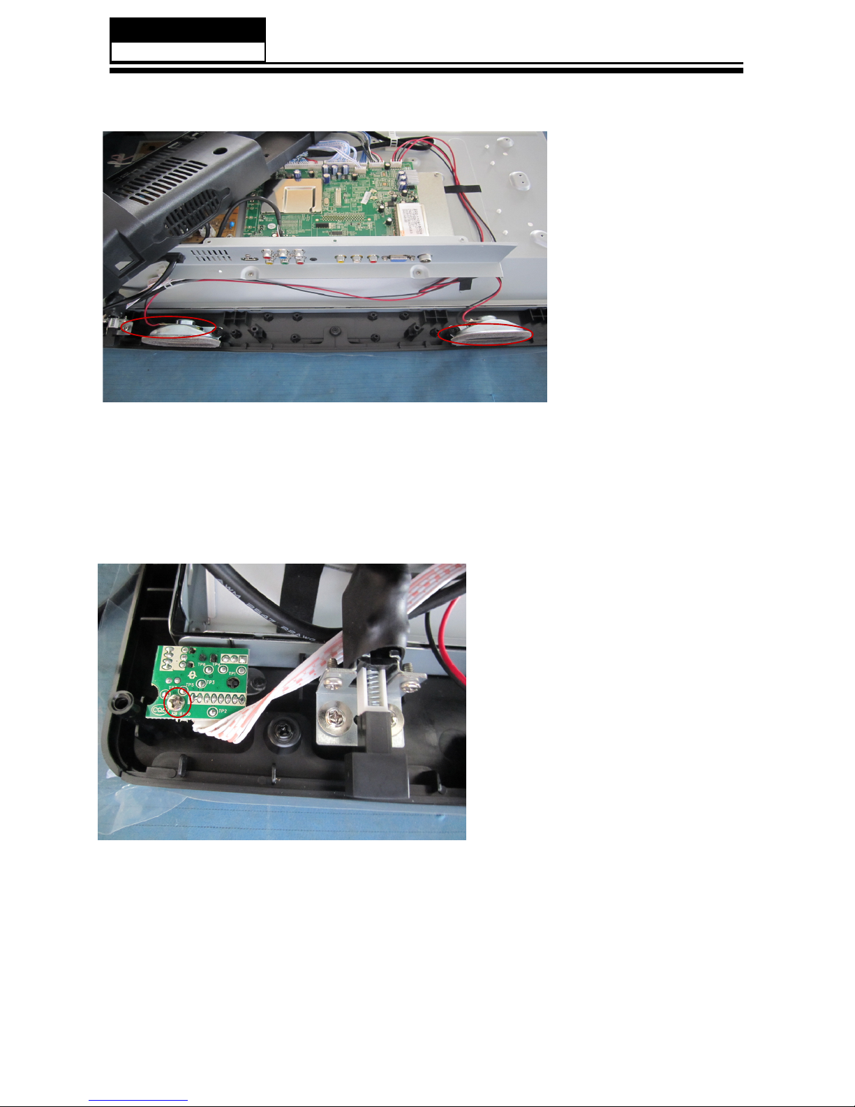
4-6 Remove the speaker
Take out the speaker
4-7 Remove the remote control
take out the remote control
board
Service Manual
Model No.:
- 17 -
Page 18
5. Installation Instructions
5-1 External Equipment Connections
Accessories
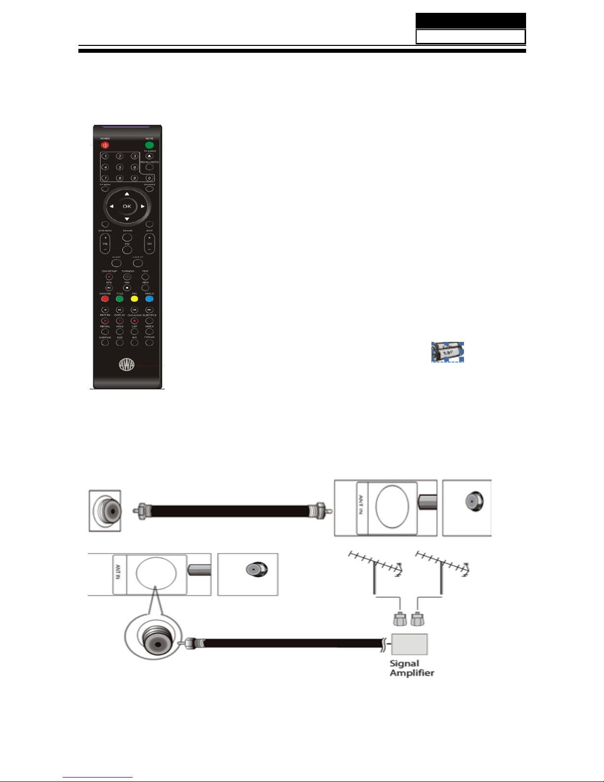
Remote Control
User GUIDE
Battery
Antenna Connection
Connect one end of a coaxial cable (not included) to the ANT IN jack on the back of
your TV/DVD combo, then connect the other end of the cable into the antenna or cable
TV wall outlet.
To improve picture quality from an antenna in a poor signal area, install a signal
amplier.
If you need to split the antenna signal to connect two TVs, install a two-way splitter.
Service Manual
Model No.:
- 18 -
Page 19
Service Manual
Model No.:
- 19 -
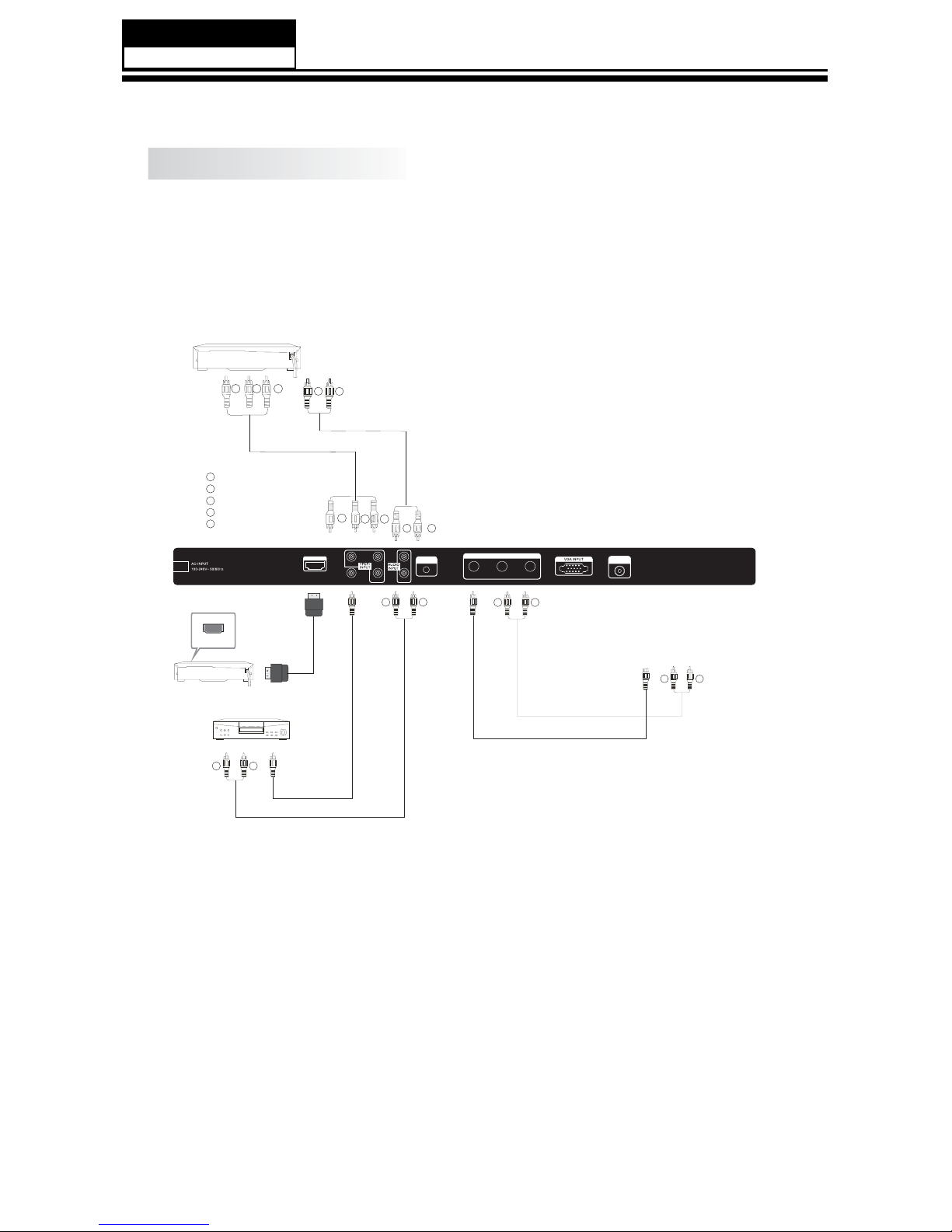
CONNECTING TO AV EQUIPMENT
It can be connected to the following appliances: VCR, multi disc player, DVD, camcorder, video
game or stereo system, etc.....
YPbPr can support these video formats: 480i,576i,480p,576p,720p,1080i.(component video)
This TV provides one group of AV, one group of YPbPr (component video) inputs for
convenient connection to VCR, DVD or other video equipment. Please refer to the owner's
manual of the equipment to be connected as well.
You can use the input terminals on TV set rear as follows.
W
R
To audio outputs
VIDEO EQUIPMENT
TO VIDEO output
W R
W R
G
B
R
G
B
R
Yellow (video)
White(audio L)
Red(audio R or Pr)
Y
W
R
Blue(Pb)
Green(Y)
B
G
HDMI
VIDEO EQUIPMENT with YPbPr
W
R
HDMI INPUT
PC
AUDIO INPUT
L
RAVPrY
Pb
AV L R
AV OUTP UT
RF INPUT
W
R
W R
TO AUDIO INPUTS
TO VIDEO
INPUTS
Page 20

Service Manual
Model No.:
- 20 -
PRESET M
ODE
HDMIINPUT
PC
AUDIO INPUT
L
RAVPrY
Pb
AV L R
AV OUTPU T
RF INPUT
STEPS:
CONNECTING TO PC
Be sure both the TV and computer are set to Power off.
1.Connect VGA and audio cable.
2.Connect the power cord.
3.Power on the TV, switch the input source to VGA mode.
4.Power on the PC.
This sequence is very important.
1
2
3
4
5
6
7
720*400
640*480
800*600
800*600
800*600
1024*768
1024*768
70
60
56
60
72
60
70
31.47
31.47
35.156
37.88
48.08
48.36
56.48
RESOLUTION
V.Freq.(Hz) H.Freq.(KHz)
Page 21

5-2 HDMI Connections
When the source device(DVD player or Set Top Box) supports HDM
How To Connect
1. Connect the source device to HDMI port of this TV with an HDMI cable(not supplied
with this product).
2. No separated audio connection is necessary.
How To Use
If the source device supports Auto HDMI function, the output resolution of the source
device will be automatically
set to 1280x720p.
If the source device does not support Auto HDMI, you need to set the output resolution
appropriately.
To get the best picture quality, adjust the output resolution of the source device to
1280x720p.
Select HDMI input source in input source option of Select Main source menu.
When the source device(DVD player or Set Top Box) supports DVI
How To Connect
1. Connect the source device to HDMI port of this TV with a HDMI-to-DVI cable(not
supplied with this product).
2. A separated audio connection is necessary.
3. If the source device has an analog audio output connector, connect the source device
audio output to DVI Audio In port located on the PC port.
How To Use
If the source device supports Auto DVI function, the output resolution of the source device
will be automatically
set to 1280x720p.
If the source device does not support Auto DVI, you need to set the output resolution
appropriately.
To get the best picture quality, adjust the output resolution of the source device to
1280x720p.
Press the INPUT button to select HDMI input source in input source option of Select Main
source menu.
Installation
Service Manual
Model No.:
- 21 -
Page 22

Cable sample
HDMI Cable
(not supplied with the product)
HDMI to DVI Cable
( not supplied with the product)
Analog Audio Cable
(Stereo to RCA type)
(not supplied with the product)
Service Manual
Model No.:
- 22 -
Page 23

Power source
TO USE AC POWER SOURCE
Use the AC polarized line cord provided for operation on AC.
Insert the AC cord plug into a standard polarized AC outlet.
NOTES:
■ Never connect the AC line cord plug to other than the specied voltage.
Use the attached power cord only.
■ If the polarized AC cord does not t into a non-polarized AC outlet,
do not attempt to le or cut the blade. It is the user`s responsibility to have an
electrician replace the obsolete outlet.
■ If you cause a static discharge when touching the unit and the unit fails to function,
simply unplug the unit from the AC outlet and plug it back in. The unit should return to
normal operation.
Service Manual
Model No.:
- 23 -
Page 24

6. Operation Instructions
6.2 Back panel controls
Service Manual
Model No.:
- 24 -
KEY BOARD
1. SOURCE:
2. MENU:
3. CH+/CH-
4. VOL+/VOL-
5.
Displays the input source Menu.
Displays the main MENU.
In TV mode, press "CH+" or "CH-" to change the
channel up and down.
In MENU mode, press "CH+" or "CH-" to select items.
Adjusts the sound level.
In MENU mode, press "VOL+" or "VOL-" to adjust the
item that you have selected.
Once the TV's main power switch has been activated,
press this button to turn the unit ON from STANDBY
mode.
STANDBY
6. USB
Press it again to turn the set back to STANDBY.
The USB memory stick should be plugged into the
unit directly. USB extension cables should not
be used to avoid failing of data transferring
and interference caused.
To access or play the files on your USB memory
stick using this USB socket on your TV, please
refer to use of the Applications Menu on page 17
of this manual.
SOURCE
MENU
CH+
CH-
VOL+
VOL-
STANDBY
USB
All the terminals are (from left to right):
AC Power input, HDMI input, YPbPr , AV composite video input,
Audio input, PC Audio input, AV output , VGA input,
Antenna socket.
.
(component video) input
(composite video and audio)
Note: 1. AV and YPbPr inputs share the Rear Audio input channel.
2. When the HDMI port receives a DVI signal, the matching audio signal is received
by the PC Audio input.
HDMI INPUT
PC
AUDIO INPUT
L
RAVPrY
Pb
AV L R
AV OUTP UT
RF INPUT
Page 25

6-3 Setting Up Your Remote Control
Service Manual
Model No.:
- 25 -
Remote control
03
REMOTE CONTROL
1
2
3
4
5
6
7
8
9
10
11
13
12
14
15
16
17
18
19
20
21
22
23
24
25
26
27
1:
POWER
:To
set the TV
to standby or
power on.
2: :In USB
mode, used as
reverse key,
in teletext
mode used as
subpage key.
3: : In
USB mode, used as forword key
, in teletext
mode used as reveal key.
4: :
Press the Play
Button in USB
Mode to begin
or continue
Playback.
5: :
Press the Pause
Button to pause
play in USB
Mode.
6:
TEXT
:To
enter or TELETEXT
.
7:
SUBTITLE
: T
o turn on
subtitles press the
subtitle button
in DTV mode.
8 : :
Displays the main
on-screen menu.
9 :
CURSOR
:
To
move within the
menu.
10:
OK
: Confirms selection.
11:
EPG
: T
o display information
about the program
being viewed
and what's on
next in DTV
mode.
12:
FAV
: T
o access your
favourite channels list
in TV or
DTV mode.
13:
VOL+/-
: T
o adjust sound
level.
14:
NUMERIC KEY
: For direct
access to channels.
15:
AUDIO
: T
o select the
available audio language
of TV programs
.
16:
MUTE
: T
o disable or
enable the sound
output.
17: : In
USB mode, used
as next key
, in teletext
mode used as
list key.
18: : In
USB mode, used
as previous key
, in teletext
mode used
as hold key
.
19: :In teletext
mode used as
index.
20:
: Press to
stop play in
USB mode.
21:
INFO
: T
o display the
program information of
the show you
are watching, press the info button.
22:
FREEZE:
Press to freeze
the picture you
are watching.
23: : Press
to display and
select the available
video sources.
24:
EXIT
: T
o return to
the previous menu
or exit menu.
25:
CH+/CH-
: T
o access the
next or previous
channels.
26:
REP
: In USB
mode,select Repeat mode.
27:
RECALL
: DTV Mode:RECALL:Jumps
to last channel
viewed.
VO
L
CH
RE
P
FREEZE
Page 26

Service Manual
Model No.:
TELETEXT
T
EXT
SELECTING A P
AGE
DIRECT ACCESS
TO THE ITEMS
INDEX
SUB PAGE
HOLD
REVEAL
P
r
ess
:
Y
ou
will obtain
:
LIST
Enter the number
of the page
required using the
0 to 9
up/down.
Example: page 120,
enter 120. The
number is displayed
top left, the
counter turns and
then the page
is displayed. Repeat
this operation to
view another page.
If the counter
continues to search,
this means
that the page
is not transmitted.
Select another number
.
Coloured buttons correspond
to the colours
at the bottom
of the
screen. The 4
coloured keys are
used to access
the items or
corresponding pages. The coloured areas flash when the item or the
page is not
yet available.
This returns to
the contents page (usually page 100).
Certain pages contain
sub-pages which are
automatically
displayed successively.
This key is
used to stop
or resume subpage acquisition. The
indication appears top
left.
To freeze the page.
To display or hide the concealed information (games solutions).
The user can
set four favourite
pages to be
directly linked to
the four
color keys. While list mode is activated, it is not possibility to use TOP
or FLOF navigation
with the colourkeys.
The favourite page
numbers
should be stored
and restored to/from
nonvolatile memory for
each
channel by the
system software.
This is used
to call or
exit teletext modes.
The summary appears
with
a list of
items that can
be accessed. Each
item has a
corresponding
3 digit page
number. If
the channel selected
does not broadcast
teletext, the indication
100 will be
displayed and the
screen will
remain blank (in
this case, exit
teletext and select
another channel).
Teletext
is an information
system broadcast by
certain channels which
can be
consulted like a
newspaper. It
also offers
access to subtitles
for viewers with
hearing
problems or who
are not familiar
with the transmission
language (cable networks,
satellite channels, etc.)
Page 27

7. Electrical parts
7-1. Block diagram
Service Manual
Model No.:
- 26 -
MSD306
1517
12
Page 28

7-2. Circuit Diagram
Service Manual
Model No.:
- 27 -
5
4
3
2
D D
C C
B B
RX3B0P
RX3B0N
RX3B1P
RX3B1N
RX3B2P
RX3B2N
RX3BCLKP
RX3BCLKN
DDC3BSDA
DDC3BSCL
HOTPLUG3
RX2B0P
RX2B0N
RX2B1P
RX2B1N
RX2B2P
RX2B2N
RX2BCLKP
RX2BCLKN
DDC2BSDA
DDC2BSCL
HOTPLUG2
RX1B0P
RX1B0N
RX1B1N
RX1B2P
RX1B2N
RX1BCLKP
RX1BCLKN
DDC1BSDA
RX1B1P
DDC1BSCL
HOTPLUG1
HDMI_E_CEC
RGB0_RIN+
RGB0_RIN-
RGB0_GIN+
RGB0_GIN-
RGB0_BIN+
RGB0_BIN-
RGB0-SOG
SC1_FS
SC1_FB
AV1-Rin
AV1-Lin
VGA_AR
VGA_AL
SCART_AV
SIDE_AV
SPDIF_O
CVBS_OUT
IRIN
YINO+
PBINO+
PRINO+
SOY
RAIN+
GAIN+
BAIN+
SOG
VSYNC
HSYNC
MUX_AR
MUX_AL
HD1R
HD1L
REAR_AV
DVD_AV
ASEL0
ISP-RXD
ISP-TXD
DVD-ON/OFF
MIUA_DQS0
MIUA_DQS0B
MIUA_DQS1
MIUA_DQS1B
MIUA_DQM1
MIUA_DQM0
MIUA_DQ[0:15]
MIUA_A[0:12]
MIUA_MCLK
MIUA_MCLKZ
MIUA_ODT
MIUA_WEZ
MIUA_MCKE
MIUA_BA1
MIUA_BA0
MIUA_BA2
MIUA_RASZ
MIUA_CASZ
OTG_DM
OTG_DP
OTG_DP1
OTG_DM1
USB_DETEC1
ON_USB1
TSSTART
TSVALID
TSCLK
TS_CLK
TS_MDI[7:0]
TS_D[7:3]
PCM_D[7:0]
TS_MOSTART
TS_MOVAL
PCM_IRQA_N
PCM_CE_N
PCM_IOWR_N
PCM_IORD_N
PCM_WE_N
PCM_A[14:0]
PCM_OE_N
PCM_REG_N
PCM_WAIT_N
PCM_RESET
PCM_CD_N
POWERON/OFF
BKLON
ADJ-PWM
LCDON
RF_AGC_SELO
#IF_OUT
IF_OUT
IF_AGC
RF_AGC
VIFP
VIFM
TV-SIFP
TV-SIFM
SIF_CTL
T_SDA
T_SCL
AV1_AL
AV1_AR
ON_USB2
CLASS_EN
AUOUTL1
AUOUTR1
AMP-Lout
AMP-Rout
HP_DET SC_AROUT
SC_ALOUT
HP_SMUTE
HP_SL
HP_SR
TS_MDO0
TS_MDO1
TS_MDO2
Page 6
06_TUNER
RF_AGC_SELO
IF_OUT
#IF_OUT
RF_AGC
IF_AGC
T_SCL
T_SDA
SIF_CTL
TV-SIFP
VIFM
VIFP
TV-SIFM
Page 10
10_MST_POWER
Page 11
11_AUDIO
HP_DET
AMP-Rout
HP_SR
HP_SL
HP_SMUTEAMP-Lout
AUOUTR1
AUOUTL1
SC_AROUT
CLASS_EN
SC_ALOUT
Page 3
03_AVIN&OUT
SPDIF_O
HP_SMUTE
HP_SL
HP_SR
SIDE_AV
CVBS_OUT
VGA_AL
VGA_AR
AV1_AL
AV1_AR
SC1_FB
SC1_FS
SC_ALOUT
SC_AROUT
SCART_AV
AV1-Lin
AV1-Rin
RGB0-SOG
RGB0_GIN+
RGB0_BIN+
RGB0_RIN+
RGB0_BIN-
RGB0_GIN-
RGB0_RIN-
Page 5
05_HDMI
RX2B1P
RX2B1N
RX1B1P
RX1B1N
RX1B0P
RX1B0N
RX1BCLKP
RX1BCLKN
DDC1BSCL
DDC1BSDA
RX2B0P
HOTPLUG1
RX1B2P
RX1B2N
RX2B0N
RX2BCLKP
RX2BCLKN
DDC2BSCL
DDC2BSDA
HDMI_E_CEC
RX3B2P
RX3B2N
RX3B1P
HOTPLUG2
RX3B1N
RX3B0P
HOTPLUG3
RX3B0N
RX3BCLKP
RX3BCLKN
RX2B2P
DDC3BSDA
RX2B2N
DDC3BSCL
Page 7
07_PCMCIA
OTG_DM
OTG_DP
OTG_DP1
OTG_DM1
USB_DETEC1
ON_USB1
TSSTART
TSVALID
TSCLK
TS_MDI[7:0]
TS_D[7:3]
TS_CLK
TS_MOSTART
TS_MOVAL
PCM_D[7:0]
PCM_A[14:0]
PCM_IRQA_N
PCM_CE_N
PCM_IOWR_N
PCM_IORD_N
PCM_WE_N
PCM_OE_N
PCM_REG_N
PCM_WAIT_N
PCM_RESET
PCM_CD_N
ON_USB2
TS_MDO0
TS_MDO1
TS_MDO2
Page 2
02_SYS_POWER
POWERON/OFF
BKLON
ADJ-PWM
LCDON
Page 9
09_MEMORT
MIUA_DQS0
MIUA_DQS0B
MIUA_DQS1
MIUA_DQS1B
MIUA_DQM1
MIUA_DQM0
MIUA_DQ[0:15]
MIUA_MCLK
MIUA_MCLKZ
MIUA_ODT
MIUA_WEZ
MIUA_MCKE
MIUA_BA1
MIUA_BA0
MIUA_A[0:12]
MIUA_BA2
MIUA_RASZ
MIUA_CASZ
Page 4
04_HD&VGA
YINO+
PBINO+
PRINO+
DVD_AV
DVD-ON/OFF
IRIN
HD1L
HD1R
REAR_AV
ISP-RXD
VSYNC
ISP-TXD
HSYNC
SOG
GAIN+
RAIN+
BAIN+
SOY
ASEL0
MUX_AR
MUX_AL
AV1_AR
AV1_AL
Page 8
08_MSD306
RX2B1P
HOTPLUG2
RX2B1N
RX2BCLKP
RX2B2P
RX2BCLKN
RX2B2N
RX2B0P
RX2B0N
DDC2BSDA
DDC2BSCL
RX3B1P
HOTPLUG3
RX3B1N
RX3BCLKP
RX3B2P
RX3BCLKN
RX3B2N
RX3B0P
RX3B0N
DDC3BSDA
DDC3BSCL
RX1B1P
HOTPLUG1
RX1B1N
RX1BCLKP
RX1B2P
RX1BCLKN
RX1B2N
RX1B0P
RX1B0N
DDC1BSDA
DDC1BSCL
HDMI_E_CEC
RAIN+
GAIN+
BAIN+
SOG
HSYNC
VSYNC
RGB0_RIN-
RGB0_RIN+
RGB0_GIN-
RGB0_GIN+
RGB0_BIN-
RGB0_BIN+
RGB0-SOG
SC1_FS
SC1_FB
PRINO+
SOY
YINO+
PBINO+
ADJ-PWM
OTG_DP
OTG_DM
OTG_DP1
OTG_DM1
IRIN
ISP-TXD
ISP-RXD
AV1-Rin
AV1-Lin
HD1L
HD1R
VGA_AR
VGA_AL
MUX_AR
MUX_AL
AMP-Rout
AMP-Lout
AUOUTL1
AUOUTR1
SPDIF_O
SCART_AV
DVD_AV
SIDE_AV
REAR_AV
CVBS_OUT
POWERON/OFF
CLASS_EN
PCM_RESET
PCM_CE_N
PCM_WE_N
PCM_CD_N
PCM_WAIT_N
PCM_IOWR_N
PCM_REG_N
LCDON
BKLON
PCM_OE_N
PCM_IORD_N
PCM_IRQA_N
TSCLK
TSVALID
TSSTART
TS_D[7:3]
TS_CLK
TS_MOVAL
TS_MOSTART
#IF_OUT
IF_OUT
IF_AGC
RF_AGC
VIFP
VIFM
TV-SIFP
TV-SIFM
SIF_CTL
T_SDA
T_SCL
MIUA_A[0:12]
MIUA_DQ[0:15]
MIUA_DQS0
MIUA_DQS0B
MIUA_DQS1
MIUA_DQS1B
MIUA_DQM0
MIUA_DQM1
MIUA_MCLK
MIUA_MCLKZ
MIUA_WEZ
MIUA_RASZ
MIUA_MCKE
MIUA_CASZ
MIUA_BA0
MIUA_BA1
MIUA_BA2
MIUA_ODT
TS_MDI[7:0]
PCM_A[14:0]
PCM_D[7:0]
RF_AGC_SELO
DVD-ON/OFF
ASEL0
ON_USB1
USB_DETEC1
HP_DET
ON_USB2
TS_MDO0
TS_MDO1
TS_MDO2
Page 29

Service Manual
Model No.:
- 28 -
5
5
4
4
3
3
2
2
1
1
D
D
C
C
B
B
A
A
V8ADJ
V8ADJ
V8ADJ
V8ADJ
1.32V5VA
GND
GND
+12V +8V
GND
1.8VA
1.8VA
3.3VU5Vstb
3.3VA
5VA
2.5VA
1.32V
2.5VA
5VA
3.3VA
1.8VA
3.3VU
3.3VA
SHEN ZHEN MTC MULTIMEDIA CO.,LTD
DESIGN:YANXUEWU
MODEL: MSDV3205-L2 TITLE:MST_POWER
CHECKED: PART NO.: DWG NO.:
APPRD: SHEET: 10 OF 12 VER:1.0
MSD306 POWER SUPPLY
8.12V
1.27V
1.02A
+1.2V FOR MST CORE
U37靠近CA16
放置
230mA(DDR2/PCS)
3.29V/380mA
1.31V/1100mA
3.29V/150mA
2.54V/230mA
1.84V/110mA
1.31V
C154
15nF
C154
15nF
ADJ
OUT
IN
U12
AMS1117-3.3
ADJ
OUT
IN
U12
AMS1117-3.3
321
4
C132
NC/0.1u
C132
NC/0.1u
R279
470R
R279
470R
C127
0.1u
C127
0.1u
C165
10uF
C165
10uF
C140
0.1u
C140
0.1u
C128
NC/0.1u
C128
NC/0.1u
R280 2KR280 2K
U16
MP1482
U16
MP1482
EN
7
FB
5
VCC2BS
1
SW
3
AGND
4
SS
8
COMP
6
R2731kR273
1k
C162 15nFC162 15nF
R281
6.8K
R281
6.8K
C141
0.1u
C141
0.1u
C123
0.1u
C123
0.1u
C142
0.1u
C142
0.1u
ADJ
OUT
IN
U11
AMS1117-3.3
ADJ
OUT
IN
U11
AMS1117-3.3
321
4
C137
0.1u
C137
0.1u
C135
0.1u
C135
0.1u
C158
0.1u
C158
0.1u
+
C163 470uF/16V+C163 470uF/16V
C152
100uF/16V
C152
100uF/16V
C134
NC/0.1u
C134
NC/0.1u
C159 1nFC159 1nF
R2741KR274
1K
+
C131
220uF/16V
+
C131
220uF/16V
C143
0.1u
C143
0.1u
C121
0.1u
C121
0.1u
R282
4.7K
R282
4.7K
C138
0.1u
C138
0.1u
C151
0.1uF
C151
0.1uF
+
C150
100uF/16V
+
C150
100uF/16V
C148
0.1u
C148
0.1u
R278
100K
R278
100K
+
C126
100uF/16V
+
C126
100uF/16V
C124
0.1u
C124
0.1u
C133
0.1u
C133
0.1u
C144
0.1u
C144
0.1u
+
C136
100uF/16V
+
C136
100uF/16V
R269NCR269
NC
C157
0.1u
C157
0.1u
C139
NC/0.1u
C139
NC/0.1u
R277
2.49K/%1
R277
2.49K/%1
C153
0.1uF
C153
0.1uF
R2700RR270
0R
R271NCR271
NC
C125
NC/0.1u
C125
NC/0.1u
C122
0.1u
C122
0.1u
R275
470R
R275
470R
C164 0.1uC164 0.1u
C146
0.1u
C146
0.1u
L80
15H_2A
L80
15H_2A
C156
0.1u
C156
0.1u
C160
10uF
C160
10uF
ADJ
OUT
IN
U14
AMS1117-ADJ
ADJ
OUT
IN
U14
AMS1117-ADJ
321
4
ADJ
OUT
IN
U13
AMS1117-ADJ
ADJ
OUT
IN
U13
AMS1117-ADJ
321
4
U15
AMS1084-SO263
TO-252-4
U15
AMS1084-SO263
TO-252-4
Adjust
1
VIN3VOUT
2
TAB
4
R2720RR272
0R
C130
0.1u
C130
0.1u
C147
0.1u
C147
0.1u
+
C129
100uF/16V
+
C129
100uF/16V
C155
0.1u
C155
0.1u
C145
0.1u
C145
0.1u
C149
0.1u
C149
0.1u
R276
220R
R276
220R
C161 0.1uC161 0.1u
Page 30

Service Manual
Model No.:
- 29 -
5
4
3
2
D
C
B
HP_LINP
ROUT+
LOUT+
ROUT#
HP_RINP#
ROUT#
HP_LINP#
SVRR
LOUT#
SC_AROUT
ROUT-
ROUT-
ROUT-
ROUT-
HP_LIN
HP_RINAMP-Rout
AMP-Lout
AUOUTR1
AUOUTL1
SC_ALOUT
HP_LIN
HP_RIN
HP_LINP#
HP_LINP#
HP_LINN#
HP_LINN#
LOUT+
LOUT+
LOUT+
LOUT+
LOUT-
HP_RINP#
HP_RINN#
ROUT-
LOUT-
ROUT+
MUTEn
VCC-OP2
VCC-OP2
HP_RINP
LOUT#
LOUT#
SVRR
MUTEO
MUTETI
ROUT-
ROUT+
LOUT1+#
LOUT1-#
GAIN1
GAIN0
LOUT-GAIN0
GAIN1
VOLUME
AMP1_R-
AMP1_R+
LOUT1-#
LOUT1+#
SUB_AL+ AMP1_L+
AMP1_L-
SD
VOLUME
LOUT2-#
FADE
LOUT2+#
+12V
SD
FADE
HP_RINP
HP_LINP
SUB_AL+
SUB_AL-
LOUT+
LOUT-
LOUT+
HP_LINP#
HP_LINN# AMP1_L-
HP_RINP#
HP_RINN# AMP1_R-
AMP1_R+
AMP1_L+
AMP2_L-
AMP2_L+HP_LINP#
HP_LINN#
SUB_AL-
AMP2_L+
AMP2_L-
AMP2_R+
AMP2_R-HP_RINN#
HP_RINP#
AMP2_R-
AMP2_R+
LOUT2-#
LOUT2+#
SUB_LOUT-
SUB_LOUT+
ROUT+
LOUT+
MUTEO
MUTEPAM
MUTEO
ROUT-
MUTEPAM
CLASS_EN
MUTEPAM
MUTEPAM
HP_RIN
HP_LIN
HP_DETHP_DET HP_SMUTE
HP_SL
HP_SR
AMP-Rout
AMP-Lout
AUOUTR1
AUOUTL1
SC_AROUT
CLASS_EN
SC_ALOUT
HP_DET
HP_SR
HP_SL
HP_SMUTE
+8V
PVCC
+8V
PVCC
+12V
PVCC
PVCC
+5V
PVCC
3.3VA
+8V
3.3VA
+12V
+12V
+12V+12V
+12V
+12V
+12V
+8V
+8V
+8V
+8V
+12V
PVCC
3.3VA
GND
GND GND
+5V
+5V
GND GND GND
GND
GND
5VA
GND
GND
GAIN=1K/470R
Location Near
IC Pin.
Location Near
IC Pin.
AMP
AUDIO OP
MUTE Control
HOLE
Ground in the middle of the L/R
Gain=R295/R298+1
Gain=R285/R291+1
SUBWOOFER SCH
F=Q/
∏
RC
LOW PASS
PH_Drive
R351
100R
R351
100R
L90
NC/FB/1206
L90
NC/FB/1206
R307
NC/0R
R307
NC/0R
L50
FB_56OHM_500MA
L50
FB_56OHM_500MA
C231
NC/220nF
C231
NC/220nF
Q30
NC/BT3904
Q30
NC/BT3904
-
+
U20B
NC/4558
-
+
U20B
NC/4558
5
6
7
8 4
R320
NC/0R
R320
NC/0R
R369
NC/1uF
R369
NC/1uF
C250
NC/1u
C250
NC/1u
R321
NC/4.7K
R321
NC/4.7K
C230
NC/10uF
C230
NC/10uF
C213
1000pF
C213
1000pF
R383
NC/100K
R383
NC/100K
C214
NC/10uF
C214
NC/10uF
R319 NC/0RR319 NC/0R
C221
200pF
C221
200pF
R291
10K
R291
10K
R367
NC/100
R367
NC/100
R327 NC/0RR327 NC/0R
R299
30K
R299
30K
R328
NC/0R
R328
NC/0R
Q29
NC/2N3904
Q29
NC/2N3904
312
+
C236
470uF/16V
+
C236
470uF/16V
1 2
R322
NC/100R
R322
NC/100R
R303
NC/0R
R303
NC/0R
R305 NC/10KR305 NC/10K
R292 3KR292 3K
C238
NC/10uF
C238
NC/10uF
C174
10uF
C174
10uF
R336
10R
R336
10R
C251
NC/100n
C251
NC/100n
C191
200pF
C191
200pF
C227
NC/1uF
C227
NC/1uF
R339
470R
R339
470R
D8 IN4148D8 IN4148
C228
NC/1uF
C228
NC/1uF
C170
0.1uF
C170
0.1uF
C302
NC/2.2uF
C302
NC/2.2uF
R338
10R/0.22uF
R338
10R/0.22uF
C176
220uF/16V
C176
220uF/16V
C222
2.2uF
C222
2.2uF
R362
10R
R362
10R
C243
0.22uF
C243
0.22uF
C200
NC/4.7uF
C200
NC/4.7uF
R345 NC/0RR345 NC/0R
R314
100K
R314
100K
R371
NC/15K
R371
NC/15K
R365
NC/100K
R365
NC/100K
R289
NC/0R
R289
NC/0R
U25
NC/DF3544
U25
NC/DF3544
IN1
3
BIAS
6
OUTA1MUTE
2
VDD
8
GND
4
IN2
5
OUTB
7
C189
NC/1000P
C189
NC/1000P
NC/0R
R370
NC/0R
R370
C209
2.2uF
C209
2.2uF
R388
NC/100
R388
NC/100
+
C241
470uF/16V+C241
470uF/16V
1 2
R352
NC/0R
R352
NC/0R
H1
10-2.54MMH110-2.54MM
123
4
R288
NC/0R
R288
NC/0R
C195
NC/220nF
C195
NC/220nF
C296
NC/10UF
C296
NC/10UF
C212
1uF
C212
1uF
C178 NC/0.22uFC178 NC/0.22uF
R3080RR308
0R
C2030RC203
0R
R373
NC/1M
R373
NC/1M
R346 150RR346 150R
C202
200pF
C202
200pF
R296
NC/0R
R296
NC/0R
R390
NC/100K
R390
NC/100K
R301 220RR301 220R
C169
0.1uF
C169
0.1uF
C190
NC/1000P
C190
NC/1000P
R337
NC/0R
R337
NC/0R
C196
NC/1uF
C196
NC/1uF
C295 NC/2.2uFC295 NC/2.2uF
U18
NC/PAM8610
U18
NC/PAM8610
AVDD3VREF4RINN1RINP
2
FADE8AGND17VOLUME5REFGND
6
PVCCL
12
PGNDL
11
LINN10LINP
9
BSLP
16
BSLN
15
LOUTN
14
LOUTN
13
LOUTP
17
LOUTP
18
PVCCL
19
PGNDL
20
VCLAMPL
21
COSC22ROSC23AGND
24
MUTE
25
AVCC
26
V2P5
27
VCLAMPR
30
PGNDR
31
PVCCR
32
ROUTP
33
ROUTP
34
BSRP
35
BSRN
36
ROUTN
37
ROUTN
38
PVCCR
39
PGNDR
40
AGND
28
SD
29
thermal
41
C232
NC/10uF
C232
NC/10uF
C244
0.22uF
C244
0.22uF
+
C210
100uF/16V+C210
100uF/16V
R335 NC/0RR335 NC/0R
C2080RC208
0R
R286
NC/0R
R286
NC/0R
R306 10KR306 10K
R313 100RR313 100R
Q32
3906
Q32
3906
C179 NC/0.22uFC179 NC/0.22uF
R325
100K
R325
100K
C182
NC/1000P
C182
NC/1000P
Q33
2N3904
Q33
2N3904
312
C187
NC/10uF
C187
NC/10uF
R315
NC/100K
R315
NC/100K
Q31
2N3904
Q31
2N3904
312
L86
NC/FB/1206
L86
NC/FB/1206
R415
NC/100K
R415
NC/100K
R386
NC/15K
R386
NC/15K
U19
TPA1517
U19
TPA1517
IN11SGND2SVRR3OUT14PGND5OUT26VCC7M/SB8IN29GND/HS
10
GND/HS11GND/HS12GND/HS13GND/HS14GND/HS15GND/HS16GND/HS17GND/HS18GND/HS19GND/HS
20
L81
NC/FB/1206
L81
NC/FB/1206
R355
NC/0R
R355
NC/0R
C217
NC/1000pF
C217
NC/1000pF
C242
NC/100n
C242
NC/100n
C197
NC/1uF
C197
NC/1uF
C225
NC/1000P
C225
NC/1000P
+
C248
220uF/16V
+
C248
220uF/16V
-
+
U20A
NC/4558
-
+
U20A
NC/4558
3
2
1
8 4
C207 NC/1uFC207 NC/1uF
R374
NC/100K
R374
NC/100K
R309
NC/0R
R309
NC/0R
L85
NC/FB/1206
L85
NC/FB/1206
R343
330R
R343
330R
C205
NC/220uF/16V
C205
NC/220uF/16V
R317
NC/10K
R317
NC/10K
R295
NC/10R
R295
NC/10R
C299
NC/10UF
C299
NC/10UF
U17
NC/TPA3110D2
U17
NC/TPA3110D2
SD1FAULT2LINP3LINN
4
AGND8AVCC7GAIN16GAIN0
5
GVDD9PLIMIT10RINN11RINP
12
BSPR
17
OUTPR
18
PGND
19
OUTNR
20
BSNR
21
BSNL
22
OUTNL
23
PGND
24
OUTPL
25
BSPL
26
PVCCL27PVCCL
28
PVCCR
16
NC13PBTL
14
PVCCR
15
GND
29
R368
NC/15K
R368
NC/15K
R311
NC/0R
R311
NC/0R
R304
NC/10K
R304
NC/10K
C183 NC/1uFC183 NC/1uF
C224
NC/1000P
C224
NC/1000P
R298
NC/10K
R298
NC/10K
R3120RR312
0R
R3341KR334
1K
C215
NC/100nF
C215
NC/100nF
C188
0.1uF
C188
0.1uF
C211 NC/1uFC211 NC/1uF
R341
NC/0.22uF
R341
NC/0.22uF
C223
1000pF
C223
1000pF
R375
NC/22K
R375
NC/22K
T1
10-2.54MMT110-2.54MM
1234567
8
R347
NC/120K
R347
NC/120K
C186 NC/0.22uFC186 NC/0.22uF
Q28
3906
Q28
3906
R342
100K
R342
100K
C204
NC/2200uF/16V
C204
NC/2200uF/16V
C300
NC/10UF
C300
NC/10UF
R357
10R/0.22uF
R357
10R/0.22uF
L88
NC/FB/1206
L88
NC/FB/1206
R354
NC/0R
R354
NC/0R
Q26
2N3904
Q26
2N3904
312
R349
75R
R349
75R
L98
NC/FB_56_OHM_4A
L98
NC/FB_56_OHM_4A
L51NCL51
NC
R382
NC/1M
R382
NC/1M
R366
NC/1.5K
R366
NC/1.5K
C216
200pF
C216
200pF
C172
NC/1000P
C172
NC/1000P
R3481KR348
1K
L82 NC/FB/1206L82 NC/FB/1206
T2
10-2.54MMT210-2.54MM
1234567
8
C206 NC/1uFC206 NC/1uF
L53
NC/FB
L53
NC/FB
RX56
NC/V800AA
RX56
NC/V800AA
R387
NC/15K
R387
NC/15K
L89
NC/FB/1206
L89
NC/FB/1206
C181 NC/1uFC181 NC/1uF
C246
NC/220n
C246
NC/220n
C301
NC/0.1uF
C301
NC/0.1uF
R324 100RR324 100R
NC/0R
R385
NC/0R
R385
R333
NC/0R
R333
NC/0R
C226
NC/1000pF
C226
NC/1000pF
R293
NC/10K
R293
NC/10K
R363 150RR363 150R
C247
NC/10uF
C247
NC/10uF
+
C180
10uF/16V/220uF/16V
+
C180
10uF/16V/220uF/16V
R377
NC/1uF
R377
NC/1uF
R340 100RR340 100R
R361
NC/0.22uF
R361
NC/0.22uF
C192
NC/10uF
C192
NC/10uF
C219 NC/220pFC219 NC/220pF
C237
NC/10uF
C237
NC/10uF
C298
NC/0.1uF
C298
NC/0.1uF
L49
NC/10K
L49
NC/10K
R356
330R
R356
330R
R331 NC/0RR331 NC/0R
C184
NC/1000P
C184
NC/1000P
J24
NC/2Pin 2.0MM
J24
NC/2Pin 2.0MM
1
2
L97
NC/FB_56_OHM_4A
L97
NC/FB_56_OHM_4A
R381
2R2
R381
2R2
R329
NC/1K
R329
NC/1K
Q34
2N3904
Q34
2N3904
312
C245
NC/47P
C245
NC/47P
C233
NC/1000P
C233
NC/1000P
C240
NC/47P
C240
NC/47P
R359
NC/0R
R359
NC/0R
L83 NC/FB/1206L83 NC/FB/1206
L52
FB_120_OHM_500MA
L52
FB_120_OHM_500MA
J26
SPEAKER
J26
SPEAKER
123
4
C185
NC/1uF
C185
NC/1uF
Q36
2N3904
Q36
2N3904
312
C220 NC/1uFC220 NC/1uF
C235
NC/220n
C235
NC/220n
C218
1uF
C218
1uF
R316
NC/0R
R316
NC/0R
C194
NC/10uF
C194
NC/10uF
+
C167
100uF/16V+C167
100uF/16V
R384
NC/1.5K
R384
NC/1.5K
C229
NC/220nF
C229
NC/220nF
C249
NC/10uF
C249
NC/10uF
C173
0.1uF
C173
0.1uF
C166 NC/0.22uFC166 NC/0.22uF
R3782KR378
2K
R294
NC/10K
R294
NC/10K
R364
75R
R364
75R
R323 NC/0RR323 NC/0R
C168
0.001uF
C168
0.001uF
R353
100K
R353
100K
R414
NC/100K
R414
NC/100K
RX57
NC/V800AA
RX57
NC/V800AA
C234
NC/1000P
C234
NC/1000P
R332
NC/1K
R332
NC/1K
R326
NC/10K
R326
NC/10K
Q27
2N3904
Q27
2N3904
312
R3762KR376
2K
C177 NC/1uFC177 NC/1uF
R300 4.7KR300 4.7K
C201
NC/0.1uF
C201
NC/0.1uF
R372
NC/33K
R372
NC/33K
C297
NC/0.1uF
C297
NC/0.1uF
L91
NC/FB/1206
L91
NC/FB/1206
R360
NC/0R
R360
NC/0R
R389
NC/33K
R389
NC/33K
R318 NC/0RR318 NC/0R
L84
NC/FB/1206
L84
NC/FB/1206
R344 10RR344 10R
R302 10KR302 10K
C239
NC/1u
C239
NC/1u
C193
NC/220nF
C193
NC/220nF
R285 270KR285 270K
R330
NC/0R
R330
NC/0R
R380
2R2
R380
2R2
R350
NC/0R
R350
NC/0R
Q35
3906
Q35
3906
R416
NC/100K
R416
NC/100K
R283
NC/0R
R283
NC/0R
R297
NC/10K
R297
NC/10K
R310
NC/10K
R310
NC/10K
R358
470R
R358
470R
C175
NC/1000P
C175
NC/1000P
R3792KR379
2K
Page 31

Service Manual
Model No.:
- 30 -
5
4
3
2
1
D
C
B
POWERON/OFF#
POWERON/OFF
BKLONBKLON
BKLON
BKLON
BKLONBKLON
ADJ-PWM
POWERON/OFF#POWERON/OFF#POWERON/OFF#POWERON/OFF#
BL_ON
BKLON
BL-ADJUST
LCDON
BL-ADJUST
BL_ON
POWERON/OFF
BKLON
ADJ-PWM
LCDON
5Vstb
5Vstb
+12V
+5V
5Vstb
VCCLCDVCCLCDFN
+12V VCCLCDFN
5Vstb
+5V
+5V
3.3VA
+5V
+5V
5VSTB#
5VA
+5V
H:ON
L:OFF
H:ON
L:OFF
552mA,V315B3_L01
1.42A
1.14A
112mA
12.21V
5.12V
PANEL POWER
TO INVERTER
5.15V
12.23V
5.12V
5.14V
R407 NC/0RR407 NC/0R
C9100pF C9100pF
Q3
2N3904Q32N3904
32
1
+
C1
470uF/16V
+
C1
470uF/16V
C3
1nFC31nF
C12
0.1uF
C12
0.1uF
J2
MAINPOWER
J2
MAINPOWER
12345678910111213
CON2
CON4-2.0mm
CON2
CON4-2.0mm
123
4
R16 1KR16 1K
Q1 AO3407Q1 AO3407
1
32
+
C17
100uF/16V
+
C17
100uF/16V
Q4
NC/2N3904Q4NC/2N3904
32
1
C22
0.1uF
C22
0.1uF
R15
4.7K
R15
4.7K
R210RR21
0R
R17 4.7KR17 4.7K
C20
0.1uF
C20
0.1uF
L57 FB_56_OHM_4AL57 FB_56_OHM_4A
+
C5
470uF/16V
+
C5
470uF/16V
R5 NCR5 NC
C6
0.1uFC60.1uF
C11
0.01uF
C11
0.01uF
R7
10KR710K
R11
10K
R11
10K
R408 NC/0RR408 NC/0R
C23
0.1uF
C23
0.1uF
R22
10k
R22
10k
C7
1nFC71nF
J25
NC/INVERTER
J25
NC/INVERTER
112233445
5
R10
10K
R10
10K
R14
4.7K
R14
4.7K
C14
0.1u
C14
0.1u
J37
DCJACK
J37
DCJACK
1
2
3
L56
FB_56_OHM_4A
L56
FB_56_OHM_4A
+
C21
470uF/16V+C21
470uF/16V
R18
4.7K
R18
4.7K
C16
0.1uF
C16
0.1uF
Q2
2N3904Q22N3904
312
Q5
2N3904Q52N3904
32
1
C25
10n
C25
10n
R13
4.7K
R13
4.7K
C15
0.1u
C15
0.1u
C18
100pF
C18
100pF
R9
4.7KR94.7K
R19 0RR19 0R
C8
4.7nFC84.7nF
C24
10n
C24
10n
R409 0RR409 0R
C2
0.1uFC20.1uF
C4 0.1uFC4 0.1uF
C13
10uF
C13
10uF
C19
100pF
C19
100pF
R4100RR410
0R
R6 0RR6 0R
R20
10k
R20
10k
R8
100KR8100K
Q6
2N3904Q62N3904
32
1
R23NCR23
NC
R12
10K
R12
10K
C10NCC10
NC
CON1
DCJACK
CON1
DCJACK
1
2
3
Page 32

Service Manual
Model No.:
- 31 -
5
4
3
2
1
D D
C C
B B
A A
SPDIF_O
SPDIFOUT
VGA_ARI
VGA_ALI
HP_SR
SIDE_AVIN
SIDE_AULIN
SIDE_AURIN
SPDIFOUT
HP_SMUTE
HP_SL
VGA_ALI
VGA_ARI
SIDE_AV
CVBS_OUT
VOUT
VGA_AL
VGA_AR
AV1_AL
AV1_AR
RGB0_GIN-
RGB0_BIN-
RGB0_RIN-
SC1_FB
Pb
Y
Y
Pb
Pr
SCART_AV
VOUT
AV1-V
Pr
AV1-L
SC1_FSO
SC_AROUT
AV1-R
SC_ALOUT
RGB0_BIN+
RGB0_GIN+
RGB0_RIN+
RGB0-SOG
AV1-L
AV1-R
AV1-Lin
AV1-Rin
SC_ALOUT
SC_AROUT
AV1-V
SIDE_AVIN
SIDE_AULIN
SIDE_AURIN
SC_AROUT
AV1-R
SC_ALOUT
AV1-L
Pb
SC1_FSOYPr
SC1_FB
VOUT
AV1-V VOUT
SC_ALOUT
SC_AROUT
SPDIF_O
HP_SMUTE
HP_SL
HP_SR
SIDE_AV
CVBS_OUT
VGA_AL
VGA_AR
AV1_AL
AV1_AR
SC1_FB
SC1_FS
SC_ALOUT
SC_AROUT
SCART_AV
AV1-Lin
AV1-Rin
RGB0-SOG
RGB0_GIN+
RGB0_BIN+
RGB0_RIN+
RGB0_BIN-
RGB0_GIN-
RGB0_RIN-
5V-IF
+8V
AGND
AGND AGND
SPDIF Output
SIDE CVBS Input
C:1uF Location near MST.IC
R:10ohm,C:1uF 47nF Location near MST.IC
Keep spacing for L/R
Keep AGND trace with signal
Keep trace width(12mil+)
AV Output
Keep spacing for L/R
Keep AGND trace with signal
Keep trace width(12mil+)
(AV+SPDIF) Output
SC1_FSO
0-2v: TV Mode
5-8v: 16:9 AV
9.5-12v: 4:3 AV
SCART
Keep AGND trace with signal
Keep spacing for L/R
R:10ohm,C:1uF 47nF Location near MST.IC
R:10ohm,C:1uF 47nF Location near MST.IC
R:10ohm,C:1uF 47nF Location near MST.IC
R44 68RR44 68R
C56 47nC56 47n
J6
NC/HeadphotoJ6NC/Headphoto
1122334
4
R57 10KR57 10K
C31
1000pF
C31
1000pF
RX2
NC/V800AA
RX2
NC/V800AA
RX5
NC/V800AA
RX5
NC/V800AA
R31 10KR31 10K
R45 68RR45 68R
RX9
NC/V800AA
RX9
NC/V800AA
RX4
NC/V800AA
RX4
NC/V800AA
R38 33RR38 33R
R50
75R
R50
75R
C28
NC/0.1uF
C28
NC/0.1uF
L58
FB_11_OHM_500MA
L58
FB_11_OHM_500MA
C30
NC/0.1uF
C30
NC/0.1uF
C34
NC/33pF
C34
NC/33pF
R48
330R
R48
330R
C54
100pF
C54
100pF
R34
10K
R34
10K
J27
SCART_24
J27
SCART_24
11223344556677889
9
1010111112121313141415151616171718181919202021212323222224
24
25
25
26
26
R30
10K
R30
10K
C41 47nC41 47n
J5
PC Audio Input
J5
PC Audio Input
12345
6
7
8
Q9
2N3904Q92N3904
32
1
RX7
NC/V800AA
RX7
NC/V800AA
C50
100pF
C50
100pF
C51
1uF
C51
1uF
C57
100pF
C57
100pF
C37
100p
C37
100p
Q7
NC/3906Q7NC/3906
1
3 2
C27
100p
C27
100p
L59
NC/FB_11_OHM_500MA
L59
NC/FB_11_OHM_500MA
R47
22K
R47
22K
R26
75R
R26
75R
C55
100pF
C55
100pF
L60
FB_11_OHM_500MA
L60
FB_11_OHM_500MA
C33 1uFC33 1uF
RX1
NC/V800AA
RX1
NC/V800AA
R40 33RR40 33R
R29
NC/220R
R29
NC/220R
C42 47nC42 47n
C38 1nC38 1n
R59 10KR59 10K
R28
NC/1K
R28
NC/1K
R56
10K
R56
10K
C48 1uFC48 1uF
RX3
NC/V800AA
RX3
NC/V800AA
R25
75R
R25
75R
R53 10KR53 10K
R36
10K
R36
10K
J34
AV-JACK-3/AV
J34
AV-JACK-3/AV
112233445
5
7
7
6
6
8
8
R33
2.2K
R33
2.2K
R55 10KR55 10K
R61
47R
R61
47R
R39 33RR39 33R
R52
75R
R52
75R
R27
NC/150R
R27
NC/150R
J33
NC/Side_AV
J33
NC/Side_AV
1122334
4
R37 0RR37 0R
J7
AV-JACK-3/AVJ7AV-JACK-3/AV
112233445
5
7
7
6
6
8
8
R35 10KR35 10K
R62
75R
R62
75R
R60
10K
R60
10K
R24 33RR24 33R
R42
75R
R42
75R
RX6
NC/V800AA
RX6
NC/V800AA
C32
1000pF
C32
1000pF
C49
100pF
C49
100pF
C36 1uFC36 1uF
C43 47nC43 47n
C47
100pF
C47
100pF
C39 47nC39 47n
C29
NC/1uF
C29
NC/1uF
R54 10KR54 10K
C52 1uFC52 1uF
J4
NC/OUTPUTJ4NC/OUTPUT
112
2
J32
NC/AV-JACK-3/AVOUT
J32
NC/AV-JACK-3/AVOUT
112233445
5
7
7
6
6
8
8
R49
75R
R49
75R
Q8
3906Q83906
1
3 2
R43
75R
R43
75R
C44 47nC44 47n
R58 10KR58 10K
C35
100p
C35
100p
R46 68RR46 68R
P1
NC/SCARTP1NC/SCART
24681012141618
20
13579111315171921
24
25
RX8
NC/V800AA
RX8
NC/V800AA
C40 47nC40 47n
R51
10K
R51
10K
C45
4.7uF/1206
C45
4.7uF/1206
C53 1uFC53 1uF
R32
NC/150R
R32
NC/150R
C26 47nC26 47n
R41
75R
R41
75R
Page 33

Service Manual
Model No.:
- 32 -
5
5
4
4
3
3
2
2
1
1
D D
C C
B B
A A
PBINO
PBIN
PBIN
PBIN
PBIN
YIN
YIN
YIN
YIN
YIN
YIN
YIN
YIN
YIN
YIN
YIN
YIN
YIN
YIN
YIN
YIN
YIN
YIN
YINO
PRINO
DVD_AVIN
IRIN
VSYNC
HD1RIN
HD1LIN
DVD_AR
DVD_AL
DVD-ON/OFF
PBIN
YIN
DVD_AVIN
HD1RIN
PRIN
PRIN
BAIN+
AV1
GAIN+
RAIN+
DVD_AV
GRED
GRED
GRED
GREDGRED
GRED
GGRN
GGRN
GGRN
GGRNGGRN
GGRN
REAR_AV
GBLUGBLU
GBLU
GBLU
GBLUGBLU
AV1
HD1LIN
ISP-RXD GSCL
GSDA ISP-TXD
GSDA
GSDA
GSDA
GSDAGSDA
GSDA
GSDA
GSDAGSDA
GSDA
GSDAGSDA
GSDA
GSDA
GSDAGSDA
GSDA
GSDA
IHS
GSCL
GSCL
HSYNC
HSYNC
HSYNC
HSYNCHSYNC
HSYNC
HSYNC
HSYNCHSYNC
HSYNC
GSDA
GSDA
GSDA
GSDAGSDA
GSDA
GSDA
GSDAGSDA
GSDA
GSDAGSDA
SOG
IVSIVSIVSIVSIVSIVSIVSIVSIVSIVSIVSIVSIVSIVSIVSIVSIVSIVS
SOY
YINO+
PRINO
PBINO+
PRINO+
PBINO
YINO
DVD_AL
ASEL0
AV1_AR
AV1_AL
DVD_AR
MUX_AR
MUX_AL
YIN
PBIN
PRIN
YINO+
PBINO+
PRINO+
DVD_AV
DVD-ON/OFF
IRIN
HD1L
HD1R
REAR_AV
ISP-RXD
VSYNC
ISP-TXD
HSYNC
SOG
GAIN+
RAIN+
BAIN+
SOY
ASEL0
MUX_AR
MUX_AL
AV1_AR
AV1_AL
AGND
+5V
VCC1
VCC1
VCC1
+8V
R & C Location near MST.IC
AV1/YPbPr/DVD INPUT
VGA INPUT
SHEN ZHEN MTC MULTIMEDIA CO.,LTD
DESIGN:YANXUEWU
MODEL: MSDV3205-L2 TITLE:HD&VGA
CHECKED: PART NO.:
DWG NO.:
APPRD: SHEET: 4 OF 12 VER:1.0
R:10ohm C:47n Location near MST.IC
C71
10uF
C71
10uFJ9
AV-JACK-3/YPbPr
J9
AV-JACK-3/YPbPr
112233445
5
7
7
6
6
8
8
R92 100KR92 100K
R83 10RR83 10R
J11
CON7
J11
CON7
1122334455667
7
R101
10K
R101
10K
C73 47nC73 47n
R103
4.7K
R103
4.7K
R76
47R
R76
47R
C821uC82
1u
C75 1uFC75 1uF
J12
PC_DB15HD_MIDDLE
J12
PC_DB15HD_MIDDLE
1
2
3
4
5
6
7
8
9
10
11
121314
15
1617
C72
0.1uF
C72
0.1uF
C76
100pF
C76
100pF
R100
10K
R100
10K
C74 1uFC74 1uF
C87
47nF
C87
47nF
R93 100KR93 100K
RX15
NC/V800AA
RX15
NC/V800AA
L66
FB_11_OHM_500MA
L66
FB_11_OHM_500MA
C80
10uF
C80
10uF
RX19NC/V800AARX19NC/V800AA
L64
FB_11_OHM_500MA
L64
FB_11_OHM_500MA
R65
10K
R65
10K
R98 33RR98 33R
R66 33RR66 33R
J8
NC/AudioJ8NC/Audio
112
2
993
3
8
8
4
4
5
5
7
7
6
6
RX18
NC/V800AA
RX18
NC/V800AA
R78 NCR78 NC
C65 1nFC65 1nF
R67
10K
R67
10K
C63 47nFC63 47nF
C79
0.1uF
C79
0.1uF
R89 100KR89 100K
R77 NCR77 NC
R107 0RR107 0R
R71
75R
R71
75R
L69
FB_11_OHM_500MA
L69
FB_11_OHM_500MA
R82 100RR82 100R
R102 0RR102 0R
R70 0RR70 0R
R68 33RR68 33R
J10
CON4
J10
CON4
1122334
4
L70
FB_11_OHM_500MA
L70
FB_11_OHM_500MA
Q10
2N3904
Q10
2N3904
312
L61
FB_11_OHM_500MA
L61
FB_11_OHM_500MA
R94 100RR94 100R
C69 47nC69 47n
C64 47nFC64 47nF
R72
75R
R72
75R
R97 33RR97 33R
RX14
NC/V800AA
RX14
NC/V800AA
L71
FB_11_OHM_500MA
L71
FB_11_OHM_500MA
C58
1uF
C58
1uF
R85 100KR85 100K
C88
1nF
C88
1nF
L67
FB_11_OHM_500MA
L67
FB_11_OHM_500MA
C6833pF C6833pF
R69 33RR69 33R
R73
75R
R73
75R
C62
100pF
C62
100pF
R104
75R
R104
75R
R86 100KR86 100K
R75
75R
R75
75R
L62
FB_11_OHM_500MA
L62
FB_11_OHM_500MA
J35
AV-JACK-3/YPbPr
J35
AV-JACK-3/YPbPr
112233445
5
7
7
6
6
8
8
C851uC85
1u
R64
10K
R64
10K
R106
75R
R106
75R
C67
33pF
C67
33pF
R74 47RR74 47R
R81
75R
R81
75R
R99
4.7K
R99
4.7K
R95 100RR95 100R
L63
FB_11_OHM_500MA
L63
FB_11_OHM_500MA
C70
100pF
C70
100pF
R105
75R
R105
75R
R87 100KR87 100K
L65
FB_56_OHM_4A
L65
FB_56_OHM_4A
R63
10K
R63
10K
C86
47nF
C86
47nF
C60 47nFC60 47nF
RX10
NC/V800AA
RX10
NC/V800AA
R79 100RR79 100R
R88 100KR88 100K
R96 33RR96 33R
C61
100pf
C61
100pf
C66
33pF
C66
33pF
RX17
NC/V800AA
RX17
NC/V800AA
RX11
NC/V800AA
RX11
NC/V800AA
R80 100RR80 100R
C59 1uFC59 1uF
U1
4052SWU14052SW
15246109
7
121415
11
13
3
168
RX13
NC/V800AA
RX13
NC/V800AA
C83
47nF
C83
47nF
RX12NC/V800AA RX12NC/V800AA
RX20
NC/V800AA
RX20
NC/V800AA
R91 100KR91 100K
R108 0RR108 0R
RX16
NC/V800AA
RX16
NC/V800AA
Page 34

- 33 -
5
4
3
2
1
D D
C C
B B
RX1B1N
RX1B1P
RX1B0N
RX1B0P
RX1B2N
RX1B2P
RX1BCLKP
RX1BCLKN
HDMI_CEC
DDC1BSDA
DDC1BSCL
RX1B1P
RX1B1N
RX1B2N
RX1B0P
RX1B0N
RX1BCLKP
RX1BCLKN
HDMI1/5V
RX1B2P
HOTPLUG2
HDMI_E_CEC
RX2B1N
RX2B1P
RX2B0N
RX2B0P
RX2B2N
RX2B2P
RX2BCLKP
RX2BCLKN
RX3B1N
RX3B1P
RX3B0N
RX3B0P
RX3B2N
RX3B2P
RX3BCLKP
RX3BCLKN
HDMI2/5V
HOTPLUG_2
DDC3BSCL
DDC3BSDA
RX3B2P
RX3B2N
RX3B1P
RX3B1N
RX3B0P
RX3B0N
RX3BCLKP
RX3BCLKN
HOTPLUG_3
HDMI3/5V
DDC2BSDA
DDC2BSCL
RX2B1P
RX2B1N
RX2B2N
RX2B0P
RX2B0N
RX2BCLKP
RX2BCLKN
RX2B2P
HOTPLUG_3
HDMI3/5V
HDMI_CEC
RX2B2P
DDC2BSCL
DDC2BSDA
RX2B2N
RX2B1P
RX2B1N
RX2B0P
RX2B0N
RX2BCLKP
RX2BCLKN
HOTPLUG_2
HDMI2/5V
HDMI_CEC
RX3B2P
DDC3BSCL
DDC3BSDA
RX3B2N
RX3B1P
RX3B1N
RX3B0P
RX3B0N
RX3BCLKP
RX3BCLKN
HOTPLUG3
HDMI_CEC
HOTPLUG1
DDC3BSCL
DDC3BSDA
RX3B2P
RX3B2N
RX3B1P
RX3B1N
RX3B0P
RX3B0N
RX3BCLKP
RX3BCLKN
HOTPLUG_3
HDMI3/5V
HDMI_CEC
RX2B1P
RX2B1N
RX1B1P
RX1B1N
RX1B0P
RX1B0N
RX1BCLKP
RX1BCLKN
DDC1BSCL
DDC1BSDA
RX2B0P
HOTPLUG1
RX1B2P
RX1B2N
RX2B0N
RX2BCLKP
RX2BCLKN
DDC2BSCL
DDC2BSDA
HDMI_E_CEC
RX3B2P
RX3B2N
RX3B1P
HOTPLUG2
RX3B1N
RX3B0P
HOTPLUG3
RX3B0N
RX3BCLKP
RX3BCLKN
RX2B2P
DDC3BSDA
RX2B2N
DDC3BSCL
5VA
HDMI1/5V
HDMI3/5V
5VA
5VA
HDMI2/5V
3.3VU
HDMI3/5V
HDMI1/5V
R113 22KR113 22K
D2
BAV70LD2BAV70L
1
2
3
C91
0.1u
C91
0.1u
RX40
NC/V800AA
RX40
NC/V800AA
Q13
3904
Q13
3904
J14
HDMI/Side
J14
HDMI/Side
DATA2+
1
DATA2 SHIELD
2
DATA2-
3
DATA1+
4
DATA1 SHIELD
5
DAT1A-
6
DATA0+
7
DATA0 SHIELD
8
DATA0-
9
CLK+
10
CLK SHIELD
11
CLK-
12
CEC
13
NC
14
SCL
15
SDA
16
DDC/CEC GND
17
+5V POWER
18
HOT PLUG
19
20
20
21
21
22
22
RX24
NC/V80010
RX24
NC/V80010
R1211KR121
1K
RX45
NC/V80010
RX45
NC/V80010
RX49
NC/V80010
RX49
NC/V80010
RX36
NC/V80010
RX36
NC/V80010
RX50
NC/V800AA
RX50
NC/V800AA
Q11
3904
Q11
3904
RX35NC/V80010 RX35NC/V80010
R112
22K
R112
22K
C92
0.1u
C92
0.1u
RX46
NC/V80010
RX46
NC/V80010
RX22
NC/V80010
RX22
NC/V80010
D3
BAV70LD3BAV70L
1
2
3
R120
NC/100R
R120
NC/100R
RX25
NC/V80010
RX25
NC/V80010
J15
DIP-20(2*10)
J15
DIP-20(2*10)
113355779
9
111113131515171719
19
224466881010121214141616181820
20
R1151KR115
1K
D4
BAV70LD4BAV70L
1
2
3
R124 22KR124 22K
R114
10K
R114
10K
R125 4.7KR125 4.7K
R111 22KR111 22K
RX47
NC/V80010
RX47
NC/V80010
RX30NC/V80010 RX30NC/V80010
Q12
3904
Q12
3904
RX34NC/V80010 RX34NC/V80010
RX41
NC/V800AA
RX41
NC/V800AA
RX43NC/V80010 RX43NC/V80010
RX38
NC/V800AA
RX38
NC/V800AA
R119
NC/47K
R119
NC/47K
R118 4.7KR118 4.7K
R116
22K
R116
22K
R1091KR109
1K
C93
0.1u
C93
0.1u
RX31NC/V80010 RX31NC/V80010
RX39NC/V800AA RX39NC/V800AA
RX42
NC/V80010
RX42
NC/V80010
RX28
NC/V80010
RX28
NC/V80010
RX48NC/V80010 RX48NC/V80010
RX27
NC/V80010
RX27
NC/V80010
RX29
NC/V80010
RX29
NC/V80010
RX51
NC/V800AA
RX51
NC/V800AA
RX23NC/V80010 RX23NC/V80010
J13
HDMI19/Rear
J13
HDMI19/Rear
1 DATA2+
20
2 DATA2 SHIELD
21
3 DATA2-
22
4 DATA1+
23
5 DATA1 SHIELD
24
6 DAT1A-
25
7 DATA0+
26
8 DATA0 SHIELD
27
9 DATA0-
28
10 CLK+
29
11 CLK SHIELD
30
12 CLK-
31
13 CEC
32
14 NC
33
15 SCL
34
16 SDA
35
17 DDC/CEC GND
36
18 +5V POWER
37
19 HOT PLUG
38
18 +5V POWER
18
GND
41
14 NC
14
1 DATA2+
1
17 DDC/CEC GND
17
8 DATA0 SHIELD
8
NC
45
2 DATA2 SHIELD
2
19 HOT PLUG
19
15 SCL
15
6 DAT1A-69 DATA0-
9
12 CLK-
12
5 DATA1 SHIELD
5
7 DATA0+
7
16 SDA
16
NC
44
3 DATA2-
3
10 CLK+
10
13 CEC
13
GND
40
4 DATA1+
4
11 CLK SHIELD
11
GND39GND42NC43GND46GND
47
RX37
NC/V800AA
RX37
NC/V800AA
R123
10K
R123
10K
R122 22KR122 22K
RX33
NC/V80010
RX33
NC/V80010
R110
10K
R110
10K
RX21
NC/V80010
RX21
NC/V80010
R117 4.7KR117 4.7K
RX26
NC/V80010
RX26
NC/V80010
J36
HDMI
J36
HDMI
DATA2+1DATA2 SHIELD2DATA2-3DATA1+4DATA1 SHIELD5DAT1A-6DATA0+7DATA0 SHIELD8DATA0-9CLK+10CLK SHIELD11CLK-12CEC13NC14SCL15SDA16DDC/CEC GND17+5V POWER18HOT PLUG
19
20
20
21
21
232322
22
RX32
NC/V80010
RX32
NC/V80010
RX44
NC/V80010
RX44
NC/V80010
Page 35

- 34 -
5
5
4
4
3
3
2
2
1
1
D
C
B
A
T_SCL
T_SDA
RF_AGC_SELO
IF_AGCIF_AGC_T
RF_AGC
IF_OUT
IF_OUT
#IF_OUT
#IF_OUT
IF_TV
#IF_OUT
IF_OUT
IF_AGC_T
T_SDA
T_SCL
RF_AGC_T
SIF_CTL
SIFP_OUT-
SIFP_OUT
IF_TV
IF_TV
TV-SIFP
TV-SIFM
VIFM
VIFP
SSDA
SSCL T_SCL
3.3VCC_T
T_SDA
SIFP_OUT
3.3VCC_TM
RF_AGC_T
VIFNS
VIFPS
SIFP_OUT-
VIFN_OUT
VIFP_OUT
VIFP_OUT
IF_OUT
#IF_OUT
VIFN_OUT
IF_AGC
RF_AGC_T
RF_AGC_SELO
IF_OUT
#IF_OUT
RF_AGC
IF_AGC
T_SCL
T_SDA
SIF_CTL
TV-SIFP
TV-SIFM
VIFM
VIFP
3.3VA
5V-IF
5V-IF VTVCC1
+8V
VTVCC1
VTVCC1
+8V VIF_8V
3.3VA
5V-IF
5V-IF
1.8VCC
3.3VCC_T
Vdd_A1.6V
3.3VCC_T
Vdd_A1.6V_D
3.3VCC_T
Vdd_A1.6V_D
3.3VCC_T
Vdd_A1.6V_D
3.3VCC_T
Vdd_A1.6V_D
3.3VCC_T
Vdd_A1.6V
5VA
3.3VCC_T
3.3VCC_T
5VA
1.8VCC
1.8VCC
449mA
5.04V
POWER FOR ATV TUNER
SHEN ZHEN MTC MULTIMEDIA CO.,LTD
DESIGN:YANXUEWU
MODEL: MSDV3205-L2 TITLE:TUNER
CHECKED: PART NO.: DWG NO.:
APPRD: SHEET: 6 OF 12 VER:1.0
PAL /DVB-T SYSTEM
RF Input
Port
Vdd_RF_VCO_LO_3V
Put on digital GND plane
301RF V7 MM 301RF V8
Pin 1 RS5 0 DNP
Pin 1 RS7 DNP 0
75 ohm Line
LNA GND
Important:
Analog GND and digital GND is still separate,
but through Paddle GND connecting them,
Vdd_IO
CLOSE IC
Close Silicon Tuner
R131
10K
R131
10K
C113
47nF
C113
47nF
R146
NC/390R
R146
NC/390R
CS20
NC/2.2uF
CS20
NC/2.2uF
RS16
NC/391
RS16
NC/391
J30J30
1
L740RL74
0R
DS1
NC/BAV99
DS1
NC/BAV99
3
1
2
LS8
NC/12nH
LS8
NC/12nH
R129
1.5K
R129
1.5K
C103
33pF
C103
33pF
LS13 NC/120ohm_FBLS13 NC/120ohm_FB
R133
NC/4.7K
R133
NC/4.7K
R1470RR147
0R
C110
NC/15nF
C110
NC/15nF
ADJ
OUT
IN
US2
NC/AMS1117-1.8
ADJ
OUT
IN
US2
NC/AMS1117-1.8
321
4
C108
NC/47nF
C108
NC/47nF
R136
NC/1k
R136
NC/1k
C102
0.001uF
C102
0.001uF
LS1
NC/120ohm_FB
LS1
NC/120ohm_FB
CS5
NC/0.1uF
CS5
NC/0.1uF
CS1
NC/0.1uF
CS1
NC/0.1uF
CS9
NC/0.1uF
CS9
NC/0.1uF
R417
NC/0R
R417
NC/0R
LS2
NC/120ohm_FB
LS2
NC/120ohm_FB
CS12
NC/1nF
CS12
NC/1nF
RS15
NC/4K7
RS15
NC/4K7
LS11
NC/220nH
LS11
NC/220nH
RS24
NC/0R
RS24
NC/0R
CS13
NC/39p
CS13
NC/39p
CS14
NC/27pF
CS14
NC/27pF
CS19
NC/0.1uF
CS19
NC/0.1uF
R134
NC/680R
R134
NC/680R
RS12NCRS12
NC
R139
NC/56R
R139
NC/56R
CS27NCCS27
NC
C107
NC/10n
C107
NC/10n
+
CS25
NC/100uF/16V
+
CS25
NC/100uF/16V
R137
NC/39R
R137
NC/39R
CS28
NC/100uF/16V
CS28
NC/100uF/16V
Y2
NC/24MHZY2NC/24MHZ
12
CS22
NC/0.1uF
CS22
NC/0.1uF
RS2
NC/391
RS2
NC/391
R132
NC/100R
R132
NC/100R
CS3
NC/0.1uF
CS3
NC/0.1uF
CS26
NC/2.2uF
CS26
NC/2.2uF
J29J29
1
RS14
NC/4K7
RS14
NC/4K7
CS16
NC/180p
CS16
NC/180p
RS7NCRS7
NC
Q15
3906
Q15
3906
1
3 2
U3
AMS1084-SO252
TO-252-4
U3
AMS1084-SO252
TO-252-4
Adjust
1
VIN3VOUT
2
TAB
4
C114
0.1uF
C114
0.1uF
R194 NC/100RR194 NC/100R
C112
NC/15nF
C112
NC/15nF
RS23 NC/0RRS23 NC/0R
L73
NC/0.82uH
L73
NC/0.82uH
C96
220uF/16V
C96
220uF/16V
RS3
NC/10K
RS3
NC/10K
CS36
NC/100nF
CS36
NC/100nF
CS30
NC/10nF
CS30
NC/10nF
RS6
NC/1M
RS6
NC/1M
R138
NC/2.2K
R138
NC/2.2K
F1
U4
NC/MXL301RF
F1
U4
NC/MXL301RF
LNA_IN
2
AS
6
IDAC
3
VDD_DNX2
1
VBATT_A3
4
VAGC2
5
VBATT_A5
7
XTAL_N
8
XTAL_P9CLK_OUT10GND_XTAL11VREG_A_OUT1
12
VDD_DNX1
31
TF_230TF_3
29
VREG_A_OUT2
28
VBATT_A2
27
VAGC1
26
NC
23
VBATT_A113SCL14SDA
15
IF_OUTP
25
VDD_IO
16
GND_DIG
17
VREG_D_OUT
18
VREG_D_IN
19
VBATT_A4
20
VDD_REF_SX
21
NC
22
IF_OUTN
24
PADDLE
33
TF_1
32
C104
33pF
C104
33pF
R196 NC/100RR196 NC/100R
R144
NC/100K
R144
NC/100K
LS5
NC/120nH
LS5
NC/120nH
LS16
NC/220nH
LS16
NC/220nH
LS10 NC/120ohm_FBLS10 NC/120ohm_FB
LS3
NC/3.6nH
LS3
NC/3.6nH
CS29
NC/100nF
CS29
NC/100nF
C111
NC/0.1uF
C111
NC/0.1uF
LS4
NC/33nH
LS4
NC/33nH
LS14 NC/120ohm_FBLS14 NC/120ohm_FB
Q19
NC/MM3904
Q19
NC/MM3904
3
1
2
R127
10K
R127
10K
C95
220uF/16V
C95
220uF/16V
R128
10K
R128
10K
CS17
NC/0.1uF
CS17
NC/0.1uF
F Conn
JS1
F Conn
JS1
1 3
4
2
5
678
9
10
C115
0.1uF
C115
0.1uF
C262
NC/4700pF
C262
NC/4700pF
CS8
NC/4700pF
CS8
NC/4700pF
CS31
NC/39pF
CS31
NC/39pF
CS34 NC/10nFCS34 NC/10nF
R135
NC/6.8K
R135
NC/6.8K
SAW
U5
NC/D9650N
SAW
U5
NC/D9650N
2
ING4OUT1
GND
3
5
OUT2
1
IN
C97
0.1uF
C97
0.1uF
Q14
100R
Q14
100R
SAW
U6
D8602F5/K6966M/D3953N
SAW
U6
D8602F5/K6966M/D3953N
2
ING4OUT1
GND
3
5
OUT2
1
IN
R126
100K
R126
100K
LS15 NC/120ohm_FBLS15 NC/120ohm_FB
CS24
NC/18pF
CS24
NC/18pF
CS10
NC/56p
CS10
NC/56p
C106
nc/15nF
C106
nc/15nF
J31J31
1
RS4
NC/391
RS4
NC/391
C99
330pF
C99
330pF
Q17
NC/1K
Q17
NC/1K
U2
TDTC-G0X1DU2TDTC-G0X1D
Body15Body
16
RF_AGC3SCL4B26SDA5DF111IF_AGC9DF210AIF
12
Body14Body13NC1B12VTU_TP7AS
8
CS23
NC/18nF
CS23
NC/18nF
J3J3
1
LS9
NC/120ohm_FB
LS9
NC/120ohm_FB
C109
NC/0.1uF
C109
NC/0.1uF
L72
FB_56OHM_4A
L72
FB_56OHM_4A
CS4
NC/1000pF
CS4
NC/1000pF
R419
NC/0R
R419
NC/0R
CS18
NC/82p
CS18
NC/82p
CS21
NC/10nF
CS21
NC/10nF
C263
NC/4700pF
C263
NC/4700pF
R130
510R
R130
510R
RS8
NC/1M
RS8
NC/1M
LS6
NC/120ohm_FB
LS6
NC/120ohm_FB
D5
NC/BA277D5NC/BA277
LS12 NC/120ohm_FBLS12 NC/120ohm_FB
R140
NC/1.5K
R140
NC/1.5K
RS25
NC/100R
RS25
NC/100R
C105
NC/10uF
C105
NC/10uF
CS39
NC/100uF/16V
CS39
NC/100uF/16V
C98
0.015uF
C98
0.015uF
CS35 NC/10nFCS35 NC/10nF
L75
2.2uH
L75
2.2uH
RS18 NC/120RRS18 NC/120R
R418
NC/0R
R418
NC/0R
RS17
NC/391
RS17
NC/391
LS7
NC/330nH
LS7
NC/330nH
CS6
NC/10nF
CS6
NC/10nF
CS32
NC/100nF
CS32
NC/100nF
Q16
N3904
Q16
N3904
3
1
2
RS9 NC/47RRS9 NC/47R
RS10
NC/0R
RS10
NC/0R
C101
0.1uF
C101
0.1uF
C94
0.1uF
C94
0.1uF
L92NCL92
NC
Q18
NC/2SC2216
Q18
NC/2SC2216
3
1
2
CS2
NC/2.2uF
CS2
NC/2.2uF
C100
0.1uF
C100
0.1uF
R143
NC/10K
R143
NC/10K
ADJ
OUT
IN
US1
NC/AMS1117-3.3
ADJ
OUT
IN
US1
NC/AMS1117-3.3
321
4
R141
NC/22R
R141
NC/22R
CS7
NC/4700pF
CS7
NC/4700pF
R142
NC/2.2K
R142
NC/2.2K
R1450RR145
0R
RS13 NC/0RRS13 NC/0R
Page 36

Service Manual
Model No.:
5
4
3
2
1
D D
C C
B B
TSVALID
PCM_CD2_N
PCM_CD_N
PCM_CD1_N
PCM_CE_N
PCM_A10
PCM_A11
PCM_A9
PCM_A8
PCM_IRQA_N
PCM_A13
PCM_A14
PCM_A12
PCM_A7
PCM_A6
PCM_A5
PCM_A4
PCM_A3
PCM_A2
PCM_A1
PCM_A0
PCM_D0
PCM_D1
PCM_D2
PCM_D7
PCM_D4
PCM_D5
PCM_D6
PCM_D3
PCM_CE_N
PCM_CD_N
PCM_OE_N
PCM_WE_N
PCM_IRQA_N
PCM_REG_N
PCM_WAIT_N
PCM_RESET
PCM_IORD_N
PCM_IOWR_N
PCM_CD2_N
PCM_CD1_N
TSSTART
TSCLK
TS_MDI0
TS_MDI1
TS_MDI2
TS_MDI3
TS_MDI4
TS_MDI5
TS_MDI6
TS_MDI7
PCM_A[14:0]
TS_MDO3
TS_MDO4
TS_MDO5
TS_MDO6
TS_MDO7
TS_MOCLK
TS_MDO2
TS_MOVAL
TS_MOSTART
TS_MDO0
TS_MDO1
PCM_IORD_N
PCM_IOWR_N
PCM_WAIT_N
PCM_RESET
PCM_REG_N
PCM_OE_N
PCM_WE_N
PCM_D[7:0]
TS_CLK
TS_D4
TS_MDO0
TS_MDO1
TS_MDO2
TS_MDO3
TS_MDO4
TS_MDO5
TS_MDO6
TS_MDO7
TS_MDO[7:0]
TS_D5
TS_D6
TS_D7
TS_D[7:3]
TS_D3
TS_MDI[7:0]
TS_MOSTART
TS_MOVAL
TS_MOCLK
DM
OTG_DP1
OTG_DM1
DP
USB_DETEC1
OTG_DP
OTG_DM
USB_DETEC1
ON_USB1
ON_USB2
OTG_DM
OTG_DP OTG_DP1
OTG_DM1
USB_DETEC1
ON_USB2
TSSTART
TSVALID
TSCLK
TS_MDI[7:0]
TS_D[7:3]
TS_CLK
TS_MOSTART
TS_MOVAL PCM_D[7:0]
PCM_A[14:0]
PCM_IRQA_N
PCM_CE_N
PCM_IOWR_N
PCM_IORD_N
PCM_WE_N
PCM_OE_N
PCM_REG_N
PCM_WAIT_N
PCM_RESET
PCM_CD_N
ON_USB1
TS_MDO2
TS_MDO1
TS_MDO0
5VA
VCC-PCMCIAVCC-PCMCIA
+5V
5VUSB1
5VUSB2
+5V
5VUSB1
5VUSB1
5VA
VCC-PCMCIA
+5V
5VUSB2
5VUSB2
3.3VA
3.3VA
3.3VA
3.3VA
CARD DETECT
PCMCIA Connector
USB Power
USB Interface
PWR CTRL 5V card
R411
10K
R411
10K
1 2
F2
NC/NSMD050F2NC/NSMD050
J16
PCMCIA_CNT
J16
PCMCIA_CNT
GND
1
D32D43D54D65D7
6
CE1#
7
A10
8
OE#
9
A11
10
A911A8
12
A1313A14
14
WE#
15
READY
16
VCC
17
VPP1
18
MIVAL
19
MICLK
20
A12
21
A722A623A524A425A326A227A128A0
29
D030D131D2
32
WP
33
GND
34
GND35CD1#36MDO337MDO438MDO539MDO640MDO741CE2#42VS1#43IORD#44IOWR#45MISTRT46MDI047MDI148MDI249MDI350VCC51VPP252MDI453MDI554MDI655MDI756MOCLK57RESET58WAIT#59INPACK60REG#61MOVAL62MOSTART63MDO064MDO165MDO266CD2#67GND
68
GND
69
GND
70
GND
71
GND
72
R160
22R
R160
22R
R173 22RR173 22R
R175 22RR175 22R
U7
PS6231/PS6232U7PS6231/PS6232
123
4
876
5
9
7 5 3 1
8 6 4 2
RP1
22RX4
7 5 3 1
8 6 4 2
RP1
22RX4
R166
NC/51K
R166
NC/51K
R401
10K
R401
10K
1 2
J1
USB1INJ1USB1IN
123
4
5 6
R174
10K
R174
10K
1 2
J19
NC/USB2IN
J19
NC/USB2IN
123
4
5 6
L93
FB_11_OHM_500MA
L93
FB_11_OHM_500MA
R1531kR153
1k
R168
NC/100K
R168
NC/100K
R159
22R
R159
22R
C117
0.1u
C117
0.1u
J18
NC/CON4
J18
NC/CON4
123
4
RX55
NC/V800AA
RX55
NC/V800AA
J17
NC/CON4
J17
NC/CON4
123
4
RX53
NC/V800AA
RX53
NC/V800AA
+
C256
NC/100uF/16V
+
C256
NC/100uF/16V
R169
10K
R169
10K
1 2
R394
NC/1K
R394
NC/1K
R161
22R
R161
22R
+
C118
100uF/16V
+
C118
100uF/16V
R1491KR149
1K
RX52
NC/V800AA
RX52
NC/V800AA
R158
22R
R158
22R
C257
10uF
C257
10uF
F1
NC/NSMD050F1NC/NSMD050
D9
BAV99LD9BAV99L
3
1
2
R1481KR148
1K
R150 100RR150 100R
RX54
NC/V800AA
RX54
NC/V800AA
- 35 -
Page 37

Service Manual
Model No.:
5
5
4
4
3
3
2
2
1
1
D D
C C
B B
A A
LVA3N
LVA3P
CI_A10 TV-SIFM
RGB0_RIN-
PCM_IRQA_N
PCM_WAIT_N
PCM_A13
MIUA_DQ0
MIUA_DQ1
MIUA_BA0
MIUA_BA1
MIUA_DQ2
AUOUTR1
MIUA_BA2
MIUA_DQ3
MIUA_DQ4
MIUA_DQ5
MIUA_DQ6
MIUA_DQ7
MIUA_ODT
MIUA_DQ8
MIUA_DQ9
MIUA_DQ10
MIUA_DQ11
MIUA_DQ12
MIUA_DQ13
MIUA_DQ14
MIUA_DQ15
PCM_A10
MIUA_A[0:12]
MIUA_DQ[0:15]
MIUA_DQS0
MIUA_DQS0B
MIUA_DQS1
MIUA_DQS1B
MIUA_DQM0
MIUA_DQM1
MIUA_MCLK
MIUA_MCLKZ
MIUA_MCKE
CI_IORD_N
MIUA_A0
MIUA_A1
MIUA_A2
MIUA_A3
MIUA_A4
MIUA_A5
MIUA_A6
MIUA_A7
MIUA_A8
MIUA_A9
MIUA_A10
MIUA_A11
MIUA_A12
MIUA_WEZ
MIUA_RASZ
MIUA_CASZ
MVERF
I2S_OUT_BCK
LVB0P
LVB0N
GIN-
RAIN+
BIN-
BAIN+
SOG
GAIN+
RIN-
PCM_OE_N
MUX_AR
MUX_AL
TS_MDI2
TS_MDI7
TS_MDI5
TS_MDI6
TS_MDI[7:0]
TS_MDI4
TS_MDI3
TS_MDI0
TS_MDI1
TSVALID
TSSTART
TS1_CK
LVB1N
LVB1P
LVB2N
LVB2P
LVBCN
LVBCP
TSCLK
LVB3N
LVB3P
LVB0N
LVB0P
PCM_RESET
RXE3+
RXE3-
RXE1-
RXE1+
RXEC+
RXEC-
RXE2+
RXE2-
RXO2+
RXO2-
RXO0-
RXO1-
RXO1+
RXO0+
RXOC-
RXO3+
RXO3-
RXOC+
TS1_D7
AUVRM
XTALO
CI_A1
PCM_A8
CI_IRQA_N
3.3VA
RGB0_BIN+
YINO-
PRINO+
PBINO-
PBINO+
SOY
YINO+
PCM_CD_N
PRINO-
TS1_D6
TV-SIFP
PCM_IORD_N
LEDG
VIFM
TS1_D0
TS1_D1
TS1_D2
TS1_D3
TS1_D4
TS1_D5
PCM_IOWR_N
AMP-Rout
AMP-Lout
OTG_DM
OTG_DP
CVBS_OUT
REAR_AV
SIDE_AV
CI_A13
TS_MOSTART0
TS_MOVAL0
TS_CLK
TS_D7
TS_D6
TS_D5
TS_D4
TS_D3
TS_D2
TS_D1
TS_D0
PCM_D0#
CI_A8
XTALI
PCM_D1#
VGA_AL
VGA_AR
PCM_D2#
RF_AGC_SEL
LCDON
SIF_CTL
POWERON/OFF
BKLON
SPDIF_O
KEY0
FLASH_WP
ADJ-PWM
PWM0
PWM1
TXD
RXD
IRDAT
HW-RST
HD1L
HD1R
RGB0_BIN-
PCM_A14
T_SCL
T_SDA
RGB0-SOG
AUVRP
AUVAG
MVERF
PCM_WE_N
AUOUTL1
LVA0P
LVA0N
PCM_CE_N
PCM_A11
CI_A8
LVA1N
LVA1P
PCM_WAIT_N
PCM_REG_N
RGB0_GIN-
CI_A10
PCM_D3
PCM_D4
PCM_D5
PCM_D6
PCM_D7
PCM_A12
PCM_A9
PCM_A0
PCM_A1
PCM_A2
PCM_A3
PCM_A4
PCM_A5
CLASS_EN
HSYNC
PCM_A[14:0]
PCM_D[7:0]
TS1_D0
TS1_D1
TS1_D7
TS1_D6
TS1_D5
TS1_D4
TS1_D3
TS1_D2
CI_IORD_N
AV1-Lin
AV1-Rin
CI_A14
CI_A13
CI_A1
RGB0_GIN+
I2S_OUT_SD
VIFP
SCART_AV
VSYNC
PCM_IRQA_N
CI_A14
LVA2N
LVA2P
TS_D[7:3]
SDA
SCL
PWM1
PWM0
I2S_OUT_MCK
I2S_OUT_SD
I2S_OUT_BCK
HW-RST
OTG_DM1
OTG_DP1
IF_AGC
CI_OE_N
LVACN
LVACP
LVA1N
CI_IRQA_N
LVA1P
LVA2N
LVA2P
LVACN
LVACP
LVA3P
LVA3N
TP3
TP2
SPI-SCK
SPI-SDO
SPI-SDI
SPI-CSN
RF_AGC
I2S_OUT_MCK
RGB0_RIN+
CI_OE_N
DVD_AV
I2S_OUT_MCK
SPI-CSNI
SPI-SCKI
SC1_FB
KEY1
SPI-SDIISPI-SDI
SPI-SDO
SPI-CSN
SPI-SCK
SPI-SDOI
FLASH_WP
LVB1P
LVB1N
LVB2P
LVB2N
LVBCP
LVBCN
LVB3N
LVB3P
RX1BCLKP
RX1BCLKN
HOTPLUG1
RX1B1P
RX1B1N
RX1B0P
RX1B0N
RX1B2N
RX1B2P
DDC1BSCL
DDC1BSDA
HDMI_E_CEC
KEY1
KEY0
KEY0
KEY0
KEY0
KEY0
KEY0
KEY0
KEY0
KEY0
KEY0
KEY0
KEY0
KEY0
KEY0
KEY0
KEY0
KEY0
KEY1-in
KEY0-in
KEY1-in
KEY0-in
GLED
RLED
IRIN
IRIN
IRDAT
IRIN
IRIN
IRIN
IRIN
IRIN
IRIN
IRIN
IRIN
IRIN
IRIN
IRIN
IRIN
IRIN
IRIN
IRIN
IRIN
RXD
TXDISP-TXD
ISP-RXD
PANEL-ON/OFF
RXE1-
RXE0-
RXEC-
RXE2-
RXE3-
RXE1+
RXE3+
RXEC+
RXE2+
RXE0+
RXO2-
RXO0-
RXO1-
RXOC-
LCD_OP
LCD_OP
RXO3-
RXO1+
RXOC+
RXO2+
RXO0+
RXO3+
PANEL-ON/OFF OVERDRIVER
OVERDRIVER
SCL
SDA
LEDG
RLED
GLED
GLED
POWERON/OFF
CLASS_EN
LCDON
DVD-ON/OFF
TP1
TP3
SPI-SDO
SPI-CSN TP1
TP2
SPI-SCK
SPI-SDI
SCL
SDA
RF_AGC_SEL RF_AGC_SELO
ASEL0
DVD-ON/OFF
ASEL0
ON_USB1
USB_DETEC1
LCD_OP
HP_DET
RX2BCLKP
RX2BCLKN
HOTPLUG2
RX2B1P
RX2B1N
RX2B0P
RX2B0N
RX2B2N
RX2B2P
DDC2BSCL
DDC2BSDA
RX3BCLKP
RX3BCLKN
HOTPLUG3
RX3B1P
RX3B1N
RX3B0P
RX3B0N
RX3B2N
RX3B2P
DDC3BSCL
DDC3BSDA
EEP_WP
ON_USB2
RLED
GLED
STANDBY
IRIN
KEY0-in
KEY1-in
LVA0N
LVA0P
RXE0-
RXE0+
PCM_A6
PCM_A7 A7
A6
A6
A7
SC1_FS
STANDBY
#IF_OUT
IF_OUT
TS_MOSTART0TS_MOSTART
TS_MOVAL TS_MOVAL0
PCM_D0 PCM_D0#
PCM_D1#PCM_D1
TS_MDO0 TS_D0
TS_MDO2 TS_D2
TS_D1TS_MDO1
PCM_D2 PCM_D2#
3.3VA
SDA
24C32_I2C-SCL SCL
EEP_WP
24C32_I2C-SDA
RX1B1P
HOTPLUG1
RX1B1N
RX1BCLKP
RX1B2P
RX1BCLKN
RX1B2N
RX1B0P
RX1B0N
DDC1BSDA
DDC1BSCL
HDMI_E_CEC
RAIN+
GAIN+
BAIN+
SOG
HSYNC
VSYNC
RGB0_RIN-
RGB0_RIN+
RGB0_GIN-
RGB0_GIN+
RGB0_BIN-
RGB0_BIN+
RGB0-SOG
SC1_FB
PRINO+
SOY
YINO+
PBINO+
ADJ-PWM
OTG_DP
OTG_DM
OTG_DP1
OTG_DM1
IRIN
ISP-TXD
ISP-RXD
AV1-Rin
AV1-Lin
HD1L
HD1R
VGA_AR
VGA_AL
MUX_AR
MUX_AL
AMP-Rout
AMP-Lout
AUOUTL1
AUOUTR1
SPDIF_O
SCART_AV
DVD_AV
SIDE_AV
REAR_AV
CVBS_OUT
POWERON/OFF
CLASS_EN
PCM_RESET
PCM_CE_N
PCM_WE_N
PCM_CD_N
PCM_WAIT_N
PCM_IOWR_N
PCM_REG_N
LCDON
BKLON
PCM_OE_N
PCM_IORD_N
PCM_IRQA_N
TSCLK
TSVALID
TSSTART
TS_D[7:3]
TS_CLK
#IF_OUT
IF_OUT
IF_AGC
RF_AGC
VIFP
VIFM
TV-SIFP
TV-SIFM
SIF_CTL
T_SDA
T_SCL
MIUA_A[0:12]
MIUA_DQ[0:15]
MIUA_DQS0
MIUA_DQS0B
MIUA_DQS1
MIUA_DQS1B
MIUA_DQM0
MIUA_DQM1
MIUA_MCLK
MIUA_MCLKZ
MIUA_WEZ
MIUA_RASZ
MIUA_MCKE
MIUA_CASZ
MIUA_BA0
MIUA_BA1
MIUA_BA2
MIUA_ODT
TS_MDI[7:0]
PCM_A[14:0]
PCM_D[7:0]
RF_AGC_SELO
PCM_IRQA_N
DVD-ON/OFF
PCM_WAIT_N
ASEL0
DVD-ON/OFF
ASEL0
ON_USB1
USB_DETEC1
HP_DET
RX2B1P
HOTPLUG2
RX2B1N
RX2BCLKP
RX2B2P
RX2BCLKN
RX2B2N
RX2B0P
RX2B0N
DDC2BSDA
DDC2BSCL
RX3B1P
HOTPLUG3
RX3B1N
RX3BCLKP
RX3B2P
RX3BCLKN
RX3B2N
RX3B0P
RX3B0N
DDC3BSDA
DDC3BSCL
SC1_FS
TS_MOSTART
TS_MOVAL
TS_MDO0
TS_MDO2
TS_MDO1
ON_USB2
3.3VA
5V-IF
1.32V
2.5VA
5V-IF
1.8VA
3.3VU
5VA
3.3VA
3.3VU
5V-IF
1.8VA
5Vstb
3.3VU
5Vstb
5Vstb
VCCLCD
VCCLCD
3.3VA
VCCLCD
3.3VA
5Vstb
5Vstb
3.3VU 3.3VA3.3VA
3.3VU
3.3VU 3.3VU
5Vstb
3.3VA
PCMCIA IO
MSD306
靠近
MSD306
放置
靠近
MSD306
放置
靠近
MSD306
放置
Mode Selection
RESET
FLASH
KEY PAD
close to IC side
DEBUG PORT
LVDS CONNECTOR
LED_CTRL
I/O
靠近
MSD306
放置
SHEN ZHEN MTC MULTIMEDIA CO.,LTD
DESIGN:YANXUEWU
MODEL: MSDV3205-L2 TITLE:MSD306
CHECKED:
PART NO.: DWG NO.:
APPRD:
SHEET: 8 OF 12 VER:1.0
加大电容值会对低噪有帮助
Close MSD306 IC
EEPROM
I2C address
at A0.
C2601uC260
1u
R182 22RR182 22R
C290 0RC290 0R
R185
22R
R185
22R
J20
2*20PIN
J20
2*20PIN
GND
1
GND
2
RO0-
3
RO0+
4
RO1-
5
RO1+
6
RO2-
7
RO2+
8
ROC-
9
ROC+
10
RO3-
11
RO3+
12
RO4-
13
RO4+
14
GND
15
GND
16
RE0-
17
RE0+
18
RE1-
19
RE1+
20
RE2-
21
RE2+
22
REC-
23
REC+
24
RE3-
25
RE3+
26
RE4-
27
RE4+
28
GND
29
GND
30
LCDOP
31
GND
32
VCC
33
VCC
34
VCC
35
VCC
36
VCC
37
VCC
38
OP1
39
OP2
40
C270 47nC270 47n
R257
4.7K
R257
4.7K
R423
10K
R423
10K
C283
0.1u
C283
0.1u
R231 1KR231 1K
C261
0.1u
C261
0.1u
HDMI
AUDIO
I2S
SPDIF
U8C MSD306
HDMI
AUDIO
I2S
SPDIF
U8C MSD306
PAD_LINEIN_L0
N5
PAD_LINEIN_R0
L4
PAD_LINEIN_L1
R5
PAD_LINEIN_R1
T6
PAD_LINEIN_L2
P6
PAD_LINEIN_R2
P5
PAD_LINEIN_L5
T4
PAD_LINEIN_R5
T5
PAD_RX0N_AE2PAD_RX0P_AF3PAD_RX1N_AF2PAD_RX1P_AG3PAD_RX2N_AG2PAD_RX2P_AG1PAD_RXCN_AE3PAD_RXCP_AE1DDCDA_CKH5DDCDA_DAH6PAD_HOTPLUGA
J6
PAD_RX0N_BB2PAD_RX0P_BB1PAD_RX1N_BC2PAD_RX1P_BC1PAD_RX2N_BD2PAD_RX2P_BD1PAD_RXCN_BA2PAD_RXCP_BC3DDCDB_CKJ5DDCDB_DAK4HOTPLUGB
K5
PAD_CEC
H4
PAD_LINEOUT_L0
N6
PAD_LINEOUT_R0
R6
PAD_EARPHONE_OUTL
U10
PAD_EARPHONE_OUTR
V10
PAD_VRP
W4
PAD_VAG
W3
AVSS_VRM_ADC_DAC
W2
PAD_I2S_OUT_MCK
D4
PAD_I2S_OUT_SD
D6
PAD_I2S_OUT_WS
F4
PAD_I2S_IN_BCK(USB0_OCD)
E4
PAD_I2S_IN_SD(USB0_CTL)
C4
PAD_I2S_IN_WS
D3
PAD_SPDIF_OUT
P4
PAD_I2S_OUT_BCK
F5
PAD_LINEOUT_L3
V12
PAD_LINEOUT_R3
U12
PAD_RX0N_CY7PAD_RX0P_CW8PAD_RX1N_CY8PAD_RX1P_CW9PAD_RX2N_CY9PAD_RX2P_C
AA9
PAD_RXCN_CW7PAD_RXCP_C
AA7
DDCDC_CKU9DDCDC_DAV9HOTPLUGC
AA6
R245
100K
R245
100K
R248 22RR248 22R
R413 100RR413 100R
C292
150pF
C292
150pF
R198
10k
R198
10k
C278
15pF
C278
15pF
C293 0.1uFC293 0.1uF
R235
4.7K
R235
4.7K
R237
4.7K
R237
4.7K
R261 4.7KR261 4.7K
L94
120nH
L94
120nH
R190
22R
R190
22R
R186 22RR186 22R
C291 0RC291 0R
R183
22R
R183
22R
Q23
3904
Q23
3904
C272
47n
C272
47n
R253 100R253 100
L78
FB220/100mA
L78
FB220/100mA
R227 NC/1KR227 NC/1K
CS37
NC/22pF
CS37
NC/22pF
7
5
3
1
8
6
4
2
RP13
22RX4
7
5
3
1
8
6
4
2
RP13
22RX4
R258 10KR258 10K
R240
4.7K
R240
4.7K
R238
4.7K
R238
4.7K
C2771nC277
1n
R246 22RR246 22R
7
5
3
1
8
6
4
2
RP4
22RX4
7
5
3
1
8
6
4
2
RP4
22RX4
C286
0.1uF
C286
0.1uF
TS1
TS0
PCMCIA
FRONT
E
ND
U8B MSD306
TS1
TS0
PCMCIA
FRONT
E
ND
U8B MSD306
PAD_PCM_D[0]
K21
PAD_PCM_D[1]
L19
PAD_PCM_D[2]
M19
PAD_PCM_D[3]
T13
PAD_PCM_D[4]
U14
PAD_PCM_D[5]
V15
PAD_PCM_D[6]
V13
PAD_PCM_D[7]
V18
PAD_PCM_A[0]
R19
PAD_PCM_A[1]
P19
PAD_PCM_A[2]
N21
PAD_PCM_A[3]
N19
PAD_PCM_A[4]
V20
PAD_PCM_A[5]
U20
PAD_PCM_A[6]
T20
PAD_PCM_A[12]
R20
PAD_PCM_A[8]
P17
PAD_PCM_A[9]
N18
PAD_PCM_A[11]
V16
PAD_PCM_A[13]
R17
PAD_PCM_A[10]
U17
PAD_PCM_A[7]
T19
PAD_TS1_CLK
Y20
PAD_TS1_SYNC
R16
PAD_TS1_VLD
W20
PAD_TS1_D[0]
P18
PAD_TS1_D[1]
R18
PAD_TS1_D[2]
T18
PAD_TS1_D[3]
W19
PAD_TS1_D[4]
Y21
PAD_TS1_D[5]
Y19
PAD_TS1_D[6]
R21
PAD_TS1_D[7]
T21
PAD_TS0_CLK
U19
PAD_TS0_SYNC
K19
PAD_TS0_VLD
P20
PAD_TS0_D[0]
K20
PAD_TS0_D[1]
L20
PAD_TS0_D[2]
M20
PAD_TS0_D[3]
T14
PAD_TS0_D[4]
U15
PAD_TS0_D[5]
U13
PAD_TS0_D[6]
T12
PAD_TS0_D[7]
U18
PAD_IP
W1
PAD_IM
Y1
PAD_TGPIO0(RF_AGC_CTRL)
AA4
PAD_TGPIO1(SIF_CTL)
Y4
PAD_TGPIO2(TUNER_SCL)
Y6
PAD_TGPIO3(TUNER_SDA)
W6
PAD_IFAGC
V5
PAD_VIFP
AA2
PAD_VIFM
Y2
PAD_RFAGC_TAGC
V4
PAD_SIFM
AA3
PAD_SIFP
Y3
PAD_PCM_RESET
V19
PAD_PCM_A[14]
T16
PAD_PCM_IRQA_N
W21
PAD_PCM_OE_N
U16
PAD_PCM_IORD_N
V17
PAD_PCM_CE_N
T17
PAD_PCM_WE_N
V21
PAD_PCM_CD_N
T15
PAD_PCM_WAIT_N
M21
PAD_PCM_IOWR_ N
P16
PAD-PCM_REG_N
N20
PAD_PCM2_CE_N(PANEL_CTL)
G21
PAD_PCM2_RESET(EPM_WP)
G20
PAD_PCM2_WAIT_N(INV_CTL)
G19
C273
0.1u
C273
0.1u
R230
10k
R230
10k
Y1
24MHZY124MHZ
1 2
C279
15pF
C279
15pF
J22
NC/KEY
J22
NC/KEY
123
7 5 3 1
8 6 4 2
RP28
22RX4
7 5 3 1
8 6 4 2
RP28
22RX4
7
5
3
1
8
6
4
2
RP3
22RX4
7
5
3
1
8
6
4
2
RP3
22RX4
RGB CVBS
U8E MSD306
RGB CVBS
U8E MSD306
PADA_BIN0MH1PADA_GIN0PJ3PADA_GIN0M
J2
PADA_SOGIN0H2PADA_RIN0M
K2
PAD_HSYNC0L6PAD_VSYNC0
L5
PADA_BIN1MN3PADA_GIN1PL2PADA_SOGIN1L1PADA_RIN1M
L3
PAD_HSYNC1M5PAD_VSYNC1
N4
PADA_BIN2MN1PADA_GIN2MP2PADA_RIN2M
R2
PADA_SOGIN2
P3
PADA_RIN0P
K3
PADA_BIN0P
H3
PADA_RIN1PK1PADA_GIN1MM3PADA_BIN1P
M2
PADA_RIN2PR3PADA_GIN2PP1PADA_BIN2P
N2
PADA_CVBS0T1PADA_CVBS4V2PADA_CVBS5
T3
PADA_CVBS_OUT1
T2
PADA_VCOM
U1
PADA_CVBS2U3PADA_CVBS1
U2
PADA_CVBS_OUT2
U4
7 5 3 1
8 6 4 2
RP5
22RX4
7 5 3 1
8 6 4 2
RP5
22RX4
L95 NC/330nHL95 NC/330nH
R193
22R
R193
22R
C265
47n
C265
47n
R215
68R
R215
68R
R236
4.7K
R236
4.7K
R204NCR204
NC
C287
2.2uF
C287
2.2uF
R200NCR200
NC
R250 10KR250 10K
C274
0.1u
C274
0.1u
R201
NC/1K
R201
NC/1K
MIUA
U8A
MSD306
MIUA
U8A
MSD306
PAD_IO[8](A_A0)
C10
PAD_IO[41](A_A1)
D21
PAD_IO[5](A_A2)
A9
PAD_IO[44](A_A3)
E20
PAD_IO[3](A_A4)
B9
PAD_IO[43](A_A5)
E19
PAD_IO[6](A_A6)
C9
PAD_IO[45](A_A7)
F20
PAD_IO[4](A_A8)
B8
PAD_IO[46](A_A9)
F19
PAD_IO[42](A_A10)
D20
PAD_IO[2](A_A11)
C8
PAD_IO[35](A_A12)
F21
PAD_IO[14](A_DQ0)
C13
PAD_IO[32(A_DQ1)
A19
PAD_IO[15](A_DQ2)
A12
PAD_IO[33](A_DQ3)
B19
PAD_IO[34](A_DQ4)
A20
PAD_IO[13](A_DQ5)
B12
PAD_IO[31](A_DQ6]
C19
PAD_IO[17](A_DQ7)
A13
PAD_IO[18](A_DQ8)
B14
PAD_IO[29](A_DQ9)
C18
PAD_IO[19](A_DQ10)
C14
PAD_IO[30](A_DQ11)
A18
PAD_IO[28](A_DQ12)
B18
PAD_IO[16](A_DQ13)
B13
PAD_IO[27](A_DQ14)
B17
PAD_IO[20](A_DQ15)
C15
PAD_IO[23](A_DQS0)
A16
PAD_IO[24](A_DQS0B)
C16
PAD_IO[21](A_DQS1)
A15
PAD_IO[22](A_DQS1B)
B15
MVREF
F18
PAD_IO[26](A_DQM0)
B16
PAD_IO[25](A_DQM1)
C17
PAD_IO[12](A_MCLK)
C12
PAD_IO[10](A_MCLKZ)
B11
PAD_IO[37](A_CKE)
C20
PAD_IO[36](A_WEZ)
B20
PAD_IO[9](A_RASZ)
B10
PAD_IO[7](A_CASZ)
A10
PAD_IO[39](A_BA0)
C21
PAD_IO[38](A_BA1)
B21
PAD_IO[40](A_BA2)
D19
PAD_IO[11](A_ODT)
C11
C266
47nF
C266
47nF
R219NCR219
NC
7 5 3 1
8 6 4 2
RP7
22RX4
7 5 3 1
8 6 4 2
RP7
22RX4
L77
FB220/100mA
L77
FB220/100mA
R214
68R
R214
68R
R4210RR421
0R
C2761nC276
1n
U27
NC/24C32
U27
NC/24C32
A01A12A23GND
4
SDA
5
SCL
6
WP
7
VCC
8
R244
4.7K
R244
4.7K
R232
10k
R232
10k
R213
68R
R213
68R
C304NCC304
NC
Q24
3906
Q24
3906
R256 100RR256 100R
R216
68R
R216
68R
R184
22R
R184
22R
C2841uC284
1u
R225 1KR225 1K
D6
BAV99D6BAV99
3
1
2
R242
4.7K
R242
4.7K
R207
10k
R207
10k
R205
4.7K
R205
4.7K
7 5 3 1
8 6 4 2
RP9
0RX4
7 5 3 1
8 6 4 2
RP9
0RX4
R260 100RR260 100R
C267 47nC267 47n
R247 10KR247 10K
R181 22RR181 22R
7 5 3 1
8 6 4 2
RP15
22RX4
7 5 3 1
8 6 4 2
RP15
22RX4
R202NCR202
NC
7 5 3 1
8 6 4 2
RP6
22RX4
7 5 3 1
8 6 4 2
RP6
22RX4
R252 10KR252 10K
R251 10KR251 10K
C268
47n
C268
47n
R208
68R
R208
68R
R195
22R
R195
22R
R239
4.7K
R239
4.7K
L79
FB220/100mA
L79
FB220/100mA
R2261MR226
1M
J28IRJ28
IR
11223344556677889910
10
SOIC8
208mil
U9
W25Q32/EN25Q32A
SOIC8
208mil
U9
W25Q32/EN25Q32A
HOLD1VCC2NC13NC24NC35NC46SO16-CS7DO
8
WP/Vpp
9
VSS
10
NC511NC612NC713NC8
14
DI
15
CLK
16
SOP8-CS
17
SOP8-DO
18
SOP8-WP/Vpp
19
VSS
20
SOP8-DI
21
SOP8-CLK
22
SOP8-HOLD
23
SOP8-VCC
24
R254 10KR254 10K
R249 10KR249 10K
U8F MSD306U8F MSD306
AVDD_DDRA
F16
AVDD_DVIE8AVDD_DVI
F8
VDDC1.2V
H15
VDDC1.2V
H16
AVDD2P5_ADC
N8
AVDD_AU25
T8
AVDD_AU33J8AVDD_EAR33
H8
AVDD25_REF
P7
AVDD25_PGA
U8
AVDD_DDRA
E15
VDDP
G16
AVDD25_MOD
R7
AVDD_DDRA
E16
AVDD_DDRA
E17
AVDD25_MODR8AVDD1P2
K14
VDDP
G17
AVDD2P5_ADCN7DVDD_MIUA
H14
AVDD_LPLL_MEMPLL
G15
AVSS_PGA
V8
AVDD_DDRA
F17
VDDC1.2V
H17
VDDC1.2V
J14
VDDC1.2V
J15
VDDC1.2V
J16
VDDC1.2V
J17
AVDD25_REF
P8
DVDD_NODIE
K9
AVDD_DVIG8AVDD_DMPLLG9AVDD3P3_ADCE9AVDD3P3_ADC
F9
GNDN9GNDP9GND
J10
GND
K10
GND
M10
GND
N10
GND
P10
GND
R10
GND
D11
GND
G11
GND
H11
GND
J11
GND
K11
GND
L11
GND
M11
GND
N11
GND
P11
GND
R11
GND
D12
GND
E12
GND
F12
GND
G12
GND
H12
GND
J12
GND
K12
GND
L12
GND
M12
GND
N12
GND
P12
GND
R12
GND
D13
GND
E13
GND
F13
GND
G13
GND
H13
GND
J13
GND
L13
GND
M13
GND
N13
GND
P13
GND
R13
GND
D14
GND
E14
GND
L14
GND
M14
GND
N14
GND
P14
GND
R14
GND
D15
GND
K15
GND
L15
GND
M15
GND
N15
GND
P15
GND
R15
GND
D16
GND
K17
GND
L17
GND
M17
GND
K18
GND
L18
GND
M18
GND
K16
GND
L16
GND
M16
GND
E11
GND
F11
GND
D10
GND
E10
GND
F10
GND
G10
GND
H10
GND
L10
GNDR9GNDL9GND
M9
GNDD9GND
D18
GND
D17
GND
K13
GNDG4GNDG5GNDG6GND
AA1
C271
47n
C271
47n
C305
0.1uF
C305
0.1uF
C275
0.1u
C275
0.1u
R259
100K
R259
100K
R233 4.7KR233 4.7K
R1871KR187
1K
C269
47n
C269
47n
R217
27R
R217
27R
R211 4.7KR211 4.7K
R243
4.7K
R243
4.7K
C285
39P
C285
39P
R228 0RR228 0R
R425 100R425 100
R224 1KR224 1K
L96
NC/330nH
L96
NC/330nH
7 5 3 1
8 6 4 2
RP2
22RX4
7 5 3 1
8 6 4 2
RP2
22RX4
R255 10KR255 10K
R203NCR203
NC
R422
NC/1K
R422
NC/1K
C2591uC259
1u
R229
4.7K
R229
4.7K
R424 100R424 100
7 5 3 1
8 6 4 2
RP14
0RX4
7 5 3 1
8 6 4 2
RP14
0RX4
R206
10K
R206
10K
7 5 3 1
8 6 4 2
RP10
0RX4
7 5 3 1
8 6 4 2
RP10
0RX4
TF1TPTF1
TP
TF11TF22TF33TF4
4
TF55TF66TF77TF8
8
C303NCC303
NC
C281
100pF
C281
100pF
R199
4.7K
R199
4.7K
R209
68R
R209
68R
R191
22R
R191
22R
R212
68R
R212
68R
R234
4.7K
R234
4.7K
J23NCJ23
NC
123
R218NCR218
NC
C264
47nF
C264
47nF
R210 4.7KR210 4.7K
R189NCR189
NC
7 5 3 1
8 6 4 2
RP11
0RX4
7 5 3 1
8 6 4 2
RP11
0RX4
R1971KR197
1K
C294 0.1uFC294 0.1uF
7 5 3 1
8 6 4 2
RP8
22RX4
7 5 3 1
8 6 4 2
RP8
22RX4
R412 100RR412 100R
R223
10K
R223
10K
R4200RR420
0R
C258 NC/39pC258 NC/39p
R220
22K
R220
22K
R192
22R
R192
22R
C2881nC288
1n
7 5 3 1
8 6 4 2
RP12
0RX4
7 5 3 1
8 6 4 2
RP12
0RX4
R222
10K
R222
10K
PWM
SAR
SPI
UART/I2CS
I2CM
LVDS
GPIO_PM
IR
XTAL
RESET
GPIO_TCON
USB
U8D MSD306
PWM
SAR
SPI
UART/I2CS
I2CM
LVDS
GPIO_PM
IR
XTAL
RESET
GPIO_TCON
USB
U8D MSD306
PADA_OUTN_CH[6](PAD_R_ODD[6])
AA20
PADA_OUTP_CH[6](PAD_R_ODD[7])
AA19
PADA_OUTN_CH[7](PAD_R_ODD[4])
W18
PADA_OUTP_CH[7](PAD_R_ODD[5])
AA18
PADA_OUTN_CH[8](PAD_R_ODD[2])
Y18
PADA_OUTP_CH[8](PAD_R_ODD[3])
W17
PADA_OUTN_CH[10](PAD_G_ODD[6])
Y16
PADA_OUTP_CH[10](PAD_G_ODD[7])
AA16
PADA_OUTN_CH[9](PAD_R_ODD[0])
Y17
PADA_OUTP_CH[9](PAD_R_ODD[1])
W16
PADA_OUTN_CH[11](PAD_G_ODD[4])
W15
PADA_OUTP_CH[11](PAD_G_ODD[5])
AA15
PADA_OUTN_CH[12](PAD_G_ODD[2])
Y15
PADA_OUTP_CH[12](PAD_G_ODD[3])
W14
PADA_OUTN_CH[13](PAD_G_ODD[0])
Y14
PADA_OUTP_CH[13](PAD_G_ODD[1])
W13
PADA_OUTN_CH[14](PAD_B_ODD[6])
Y13
PADA_OUTP_CH[14](PAD_B_ODD[7])
AA13
PADA_OUTN_CH[15](PAD_B_ODD[4])
W12
PADA_OUTP_CH[15](PAD_B_ODD[5])
AA12
PADA_OUTN_CH[16](PAD_B_ODD[2])
Y12
PADA_OUTP_CH[16](PAD_B_ODD[3])
W11
PADA_OUTN_CH[17](PAD_B_ODD[0])
Y11
PADA_OUTP_CH[17](PAD_B_ODD[1])
W10
PAD_PWM0
J21
PAD_PWM1
J20
PAD_PWM2
J19
PAD_SAR0B4PAD_SAR1
C5
PAD_SPI_CKB5PAD_SPI_DIC6PAD_SPI_DO
A6
DDCA_CKK6DDCA_DAM6PAD_DDCR_CK
H19
PAD_DDCR_DA
H20
PAD_TESTPIN
H9
PAD_GPIO_PM6(BOOT_FLASH_CS)
B6
PAD_SPI_CZ(BACKUP_FLASH_CS)
C7
PAD_GPIO_PM8(FLASH_WP)
A7
PAD_IRINA4PAD_XTAL_INW5PAD_XTAL_OUT
Y5
PAD_RESET
E5
GND_EFUSE
J9
PAD_TCON0(USB1_OCD)
T9
PAD_TCON4(AMP_MUTE)
T11
PAD_DP_P0B3PAD_DM_P0
A3
PAD_TCON2(USB1_CTL)
U11
PAD_GPIO_PM1F6PAD_GPIO_PM5
E6
PAD_SAR2
V3
PAD_TCON6(PCM_5V_CTL)
T10
PAD_DP_P1
Y10
PAD_DM_P1
AA10
PAD_GPIO_PM4
B7
C282
100pF
C282
100pF
CS38
NC/22pF
CS38
NC/22pF
R188 22RR188 22R
J21
NC/IR
J21
NC/IR
11223344556
6
- 36 -
Page 38

Service Manual
Model No.:
5
4
3
2
1
D D
C C
B B
MA_DQ6
MA_DQ3
MA_DQ1
MA_DQ4
MA_DQ15
MA_DQ8
MA_DQ10
MA_DQ13
MA_A8
MA_A11
MA_WEZ
MA_ODT
MA_RASZ
MA_BA2
MA_DQ5
MA_DQ2
MA_DQ7
MA_DQ0
MA_CASZ
MA_A1
MA_A10
MA_A5
MA_MCLKZ
MA_MCLK
MA_CKE
MA_DQM0
MA_DQM1
MA_DQS0
MA_DQSB0
MA_DQS1
MA_DQSB1
MA_A9
MA_A12
MA_A7
MA_DQ11
MA_A3
MA_A0
MA_DQ12
MA_A2
MA_A4
MA_A6
MA_DQ9
MA_DQ14
A_MVERF
MIUA_RASZ
MIUA_CASZ
MA_DQS1
MA_DQSB1
A_MVERF
MA_MCLKZ
MIUA_A5
MIUA_BA2
MIUA_A7
MIUA_A3
MIUA_A1
MIUA_A12
MIUA_A9
MIUA_A10
MIUA_DQS0
MIUA_DQS0B
MA_DQS0
MA_DQSB0
MIUA_DQS1
MIUA_DQS1B
MA_DQ15
MA_DQ8
MA_DQ10
MA_DQ13
MIUA_DQ[0:15]
MIUA_DQ11
MIUA_DQ12
MIUA_DQ9
MIUA_DQ14
MA_DQ11
MA_DQ12
MA_DQ9
MA_DQ14
MA_DQ6
MA_DQ1
MA_DQ3
MA_DQ4
MIUA_DQ6
MIUA_DQ1
MIUA_DQ3
MIUA_DQ4
MIUA_DQ7
MIUA_DQ0
MIUA_DQ2
MIUA_DQ5 MA_DQ5
MA_DQ2
MA_DQ7
MA_DQ0
MIUA_DQ15
MIUA_DQ8
MIUA_DQ10
MIUA_DQ13
MA_RASZ
MA_CASZ
MA_A11
MA_A8
MIUA_A[0:12]
MA_A7
MA_A9
MA_A12
MA_A3
MA_A1
MA_A10
MA_A5
MIUA_A4
MIUA_A6
MA_A0
MA_A2
MA_BA0
MIUA_MCLK
MIUA_MCLKZ
MA_WEZ
MIUA_BA0
MA_MCLK
MIUA_WEZ
MIUA_ODT
MA_BA1
MA_ODT
MIUA_A8
MIUA_A11
MIUA_BA1
MA_CKE
MA_BA2
MA_A4
MA_A6
MIUA_A0
MIUA_A2
MIUA_MCKEMA_DQM1
MA_BA0
MA_BA1
MA_DQM0MIUA_DQM0
MIUA_DQM1
MIUA_DQS0
MIUA_DQS0B
MIUA_DQS1
MIUA_DQS1B
MIUA_DQM1
MIUA_DQM0
MIUA_DQ[0:15]
MIUA_MCLK
MIUA_MCLKZ
MIUA_ODT
MIUA_WEZ
MIUA_MCKE
MIUA_BA1
MIUA_BA0
MIUA_A[0:12]
MIUA_BA2
MIUA_RASZ
MIUA_CASZ
1.8VA
1.8VA
Close to MSD306
Close to DRAM
Close to MSD306Close to MSD306
Close to DRAM
Close to DRAM
7
5
3
1
8
6
4
2
RP26 22RX4
7
5
3
1
8
6
4
2
RP26 22RX4
R264 22RR264 22R
7 5 3 1
8 6 4 2
RP19
75RX4
7 5 3 1
8 6 4 2
RP19
75RX4
C120
0.1u
C120
0.1u
7
5
3
1
8
6
4
2
RP18
22RX4
7
5
3
1
8
6
4
2
RP18
22RX4
7
5
3
1
8
6
4
2
RP23 75RX4
7
5
3
1
8
6
4
2
RP23 75RX4
7
5
3
1
8
6
4
2
RP16
22RX4
7
5
3
1
8
6
4
2
RP16
22RX4
R267
10k
R267
10k
7
5
3
1
8
6
4
2
RP20 75RX4
7
5
3
1
8
6
4
2
RP20 75RX4
7 5 3 1
8 6 4 2
RP22 22RX4
7 5 3 1
8 6 4 2
RP22 22RX4
R268
10k
R268
10k
7
5
3
1
8
6
4
2
RP21 22RX4
7
5
3
1
8
6
4
2
RP21 22RX4
C1191nC119
1n
7
5
3
1
8
6
4
2
RP25 75RX4
7
5
3
1
8
6
4
2
RP25 75RX4
7 5 3 1
8 6 4 2
RP27 75RX4
7 5 3 1
8 6 4 2
RP27 75RX4
7
5
3
1
8
6
4
2
RP24 22RX4
7
5
3
1
8
6
4
2
RP24 22RX4
7
5
3
1
8
6
4
2
RP17
22RX4
7
5
3
1
8
6
4
2
RP17
22RX4
R265
100R
R265
100R
R266
100R
R266
100R
R263 75RR263 75R
ABCDE
F
GHJ
K
LMNPR
1 2 3 7 8 9
Vdd NC Vss
DQ14 VssQ UDM
VddQ DQ9 VddQ
DQ12 VssQ DQ11
Vdd NC Vss
DQ6 VssQ LDM
VddQ DQ1 VddQ
DQ4 VssQ DQ3
VddL Vref Vss
CKE WE#
RFU BA0 BA1
A10 A1
Vss A3 A5
A7 A9
Vdd A12 RFU
VssQ UDQS# VddQ
UDQS VssQ DQ15
VddQ DQ8 VddQ
DQ10 VssQ DQ13
VssQ LDQS# VddQ
LDQS VssQ DQ7
VddQ DQ0 VddQ
DQ2 VssQ DQ5
VssDL CK Vdd
RAS# CK# ODT
CAS# CS#
A2 A0 Vdd
A6 A4
A11 A8
RFU NC
Vss
U10
NT5TU32M16CG/NT5TU64M16DG
Vdd
A1
NC
A2
Vss
A3
DQ14
B1
VssQ
B2
UDM
B3
A4N8A6
N7
Vdd
M9
A0M8A2
M7
CS#
L8
CAS#
L7
ODT
K9
CLK#
K8
RAS#
K7
Vdd
J9
CLK
J8
VssDL
J7
DQ5
H9
VssQ
H8
DQ2
H7
VddQ
G9
DQ0
G8
VddQ
G7
DQ7
F9
VssQ
F8
LDQS
F7
VddQ
E9
LDQS#
E8
VssQ
E7
DQ13
D9
VssQ
D8
DQ10
D7
VddQ
C9
DQ8
C8
VddQ
C7
A7P2A9
P3
Vdd
R1
A12
R2
RFU
R3
VssQ
A7
UDQS#
A8
VddQ
A9
UDQS
B7
VssQ
B8
DQ15
B9
A10M2A1
M3
Vss
N1
A3N2A5
N3
VddQ
C1
DQ9
C2
VddQ
C3
DQ12
D1
VssQ
D2
DQ11
D3
Vdd
E1
NC
E2
Vss
E3
DQ6
F1
VssQ
F2
LDM
F3
VddQ
G1
DQ1
G2
VddQ
G3
DQ4
H1
VssQ
H2
DQ3
H3
VddL
J1
Vref
J2
Vss
J3
CKE
K2
WE#
K3
RFU
L1
BA0L2BA1
L3
RFU
R7
NC
R8
Vss
P9
A8
P8
A11
P7
R262 22RR262 22R
- 37 -
Page 39

Con
n
ection wire(Power for Mainboard)
Service Manual
Model No.:
7-3 .Wiring Connection Diagram
NO. Name
1
2
3
4
Connection Wire(For Remote)
Connection Wire(For Speaker
)
LVDS Wire
2
3
4
1
- 38 -
5
5
Connection Wire(Control for backlight ON/OFF )
6
7
8
9
Connection Wire(For Keyboard )
Connection Wire(For USB )
Connection Wire(For DVD POWER)
Connection Wire(For DVD)
6
7
8
9
Page 40

8.
Measurements and Adjustments
.
Service Manual
Model No.:
- 39-
OPERATION
04
I
n
s
t
a
l
l
a
t
i
o
n G
u
i
d
e
Pls press to s elect country at first , then
press OK but ton to start auto t uning .
N
O
T
E
:
A
l
l t
h
e c
h
a
n
n
e
l
s i
n
c
l
u
d
i
n
g
A
T
V
, D
T
V a
n
d R
a
d
i
o
c
a
n b
e t
u
n
i
n
g b
y o
n
e t
i
m
e
,
i
f t
h
e
T
u
n
e
T
y
p
e i
s
DTV
+A
TV .
T
h
i
s s
c
r
e
e
n o
n
l
y a
p
p
e
a
r w
h
e
n t
h
e
T
V f
i
r
s
t t
i
m
e
tu
rn o
n or re
se
t to f
ac
to
ry s
et
.Yo
u ca
n ch
oo
se
l
a
n
g
u
a
g
e a
n
d c
o
u
n
t
r
y
, a
u
t
o t
u
r
n
i
n
g p
r
o
g
r
a
m
s .
A
n
d a
f
t
e
r t
u
r
n
i
n
g t
h
e s
c
r
e
e
n w
i
l
l s
k
i
p t
o t
h
e f
i
r
s
t
DTV progra m.
1.CH ANN EL MENU
T
h
e f
i
r
s
t i
t
e
m o
f t
h
e M
E
N
U i
s c
h
a
n
n
e
l m
e
n
u
( f
o
r
T
V or D
TV s
ou
rc
e on
ly)
.
Y
ou c
an s
ea
rc
h cha
nn
el
s an
d ed
it p
ro
gr
ams h
er
e.
1).Auto tu ning:
Search all t he channels aut omatically( you can
s
e
l
e
c
t
A
T
V a
n
d D
T
V
)
T
u
n
e
Ty
p
e D
T
V
+
A
T
V
G
e
r
m
a
n
y
Gre
ec
e
Hun gary
Ita ly
Lux embou rg
N
e
t
h
e
r
l
a
n
d
s
Nor way
Po
la
nd
Por tugal
MEN U
Al
l th
e sto
re
d ch
an
ne
ls w
il
l be di
sa
pp
ea
r af
te
r
a
u
t
o t
u
n
i
n
g .
A
f
t
e
r a
u
t
o t
u
n
i
n
g , t
h
e c
h
a
n
n
e
l w
i
l
l t
u
r
n t
o
the first DTV channel.
2
)
.
D
T
V M
a
n
u
a
l t
u
n
i
n
g
:
Y
o
u c
a
n s
e
l
e
c
t a D
T
V c
h
a
n
n
e
l t
h
e
n f
i
n
d t
h
e
p
ro
gr
am i
n th
is c
han
ne
l.
P
l
s p
r
e
s
s t
o s
e
l
e
c
t t
h
e c
h
a
n
n
e
l , t
h
e
n p
r
e
s
s
O
K t
o s
e
a
r
c
h t
h
e p
r
o
g
r
a
m
s .
N
O
T
E
:
B
a
d N
o
r
m
a
l G
o
o
d m
e
a
n
s s
i
g
n
a
l i
n
t
e
n
s
i
t
y
.
S
w
i
t
z
e
r
l
a
n
d
N
ewZ e
ala n
d
N
o
r
w
a
y
P
o
l
a
n
d
P
o
r
t
u
g
a
l
Slo
ven i
a
S
p
a
i
n
S
w
e
d
e
n
C
o
u
n
t
r
y
O
K
R
u
m
a
n
i
a
R
u
s
s
i
a
n
Se
rbi a
Mor occo
T
u
n
i
s
Alg
eri a
U
K
D
a
n
s
k
D
e
u
t
s
c
h
H
r
v
a
t
s
k
i
I
t
a
l
i
a
n
o
Pleas e se le ct a n OSD Lan gu ag e
O
K
M
a
g
y
a
r
N
ed
e
rl
an
ds
N
o
r
s
k
P
o
l
s
k
i
E
n
g
l
i
s
h
C
e
s
k
y
E k
a
E
s
p
a
n
o
l
~
F
r
a
n a
i
s
P
o
r
t
u
g
u
e
s
P
y
c
c
k
C
h
a
n
n
e
l
T
u
n
i
n
g
T
V : 0 P
r
o
g
r
a
m
m
e
(
s
)
D
T
V : 0 P
r
o
g
r
a
m
m
e
(
s
)
R
a
d
i
o : 0 P
r
o
g
r
a
m
m
e
(
s
)
D
at
a: 0 Pr
og
ra
mme
(s
)
9
6
% U
H
F C
H 6
8 D
T
V
3). ATV Manual tun ing :
Yo
u ca
n ch
an
ge t
he s
ou
nd s
yst
em t
o se
ar
ch
t
h
e a
n
a
l
o
g
T
V c
h
a
n
n
e
l
s a
n
d f
i
n
e t
u
n
e t
h
e
ch
an
ne
ls , t
he
n st
or
ag
e the c
ha
nn
el
s yo
u
selected .
A
T
V M
a
n
u
a
l
T
u
n
i
n
g
Sto rage To 1
Sys tem BG
C
u
r
r
e
n
t C
H 1
Sea rch
Fin e-Tun e
Fre quenc y 255.2 5 MHz
S
av
e ME
NU
_
+
D
T
V M
a
n
u
a
l
T
u
n
i
n
g
V
H
F C
H 5
_
+
B
a
d
N
o
m
a
l
Goo
d
Pre ss OK to se arch
A
T
V Ma
nu
a
l T
u
ni
ng
P
r
o
g
r
a
m
m
e E
d
i
t
S
i
g
n
a
l I
n
f
o
r
m
a
t
i
o
n
<
>
C
HA
NN
E
L
A
ut
o T
u
ni
ng
D
T
V M
a
n
u
a
l
T
u
n
i
n
g
S
o
f
t
w
a
r
e U
p
d
a
t
e
(
U
S
B
)
S
o
f
t
w
a
r
e U
p
d
a
t
e
(
O
A
D
)
O
f
f
CI In forma tion
Page 41

Service Manual
Model No.:
- 40 -
04
Operation
<
>
B
a
l
a
n
c
e
A
u
t
o Vo
l
u
m
e
S
o
u
n
d M
o
d
e S
t
a
n
d
a
r
d
S
O
U
N
D
N
O
T
E
:
1).
Tint i
s avai
lab
le in NT
SC sys
tem on
ly.
2
)
.
T
h
e
r
e a
r
e f
o
u
r c
o
l
o
r
s t
e
m
p
e
r
a
t
u
r
e m
o
d
e
s
c
a
n b
e s
e
l
e
c
t
e
d m
e
d
i
u
m
, w
a
r
m
, c
o
o
l
,
u
s
e
r
3).Screen is available in PC mode only which,
c
a
n a
d
j
u
s
t H
o
r
i
z
o
n
t
a
l p
o
s
i
t
i
o
n
, v
e
r
t
i
c
a
l
p
o
s
i
t
i
o
n
, s
i
z
e a
n
d p
h
a
s
e
.
3.SOU ND MEN U
T
he thi
rd it
em of th
e MENU i
s the SO
UND
M
E
N
U
.
Yo
u can ad
just t
he sou
nd eff
ect h
ere su
ch as
treble, bass, balance etc.
Pre
ss to mo
ve, pr
ess O
K to adj
ust.
Note:
Auto volume: only available when the input
s
i
g
n
a
l v
o
l
u
m
e i
s t
o
o l
a
r
g
e o
r d
i
s
t
o
r
t
i
o
n
.
C
o
l
o
r
T
e
m
p
e
r
a
t
u
r
e
A
s
p
e
c
t R
a
t
i
o
N
o
i
s
e R
e
d
u
c
t
i
o
n
Scr een
P
i
c
t
u
r
e M
o
d
e S
t
a
n
d
a
r
d
<
>
P
I
C
T
U
R
E
Favourite
Press to choose the program , press FAV
button , it will show on the right side of the
p
r
o
g
r
a
m
.
C
h
o
o
s
e t
h
e F
A
V p
r
o
g
r
a
m , p
r
e
s
s
FAV button again , you can cancel the FAV,
the will disappear .
O
n
c
e y
o
u
r f
a
v
o
r
i
t
e g
r
o
u
p i
s c
r
e
a
t
e
d
, y
o
u c
a
n
press the FAV key to quickly access your favorite
channel.
T
he sec
ond i
tem of t
he MEN
U is PIC
TUR
E MENU
.
Y
ou can a
djus
t pic
ture e
ffec
t here
, suc
h as
contrast, brightness, etc.
Pre
ss to m
ove, p
ress O
K to adj
ust
.
2. PICTURE M ENU
5). CI informat ion : (op tio nal )
T
his me
nu can d
ispl
ay th
e CI car
d' s inf
orm
atio
n.
MEN U
P
i
c
t
u
r
e M
o
d
e S
t
a
n
d
a
r
d
C
o
n
t
r
a
s
t 8
2
B
ri
ght
ne
ss 50
Col
or 5
0
S
ha
rpn
es
s 50
Tin
t 50
C
o
l
o
r
T
e
m
p
e
r
a
t
u
r
e M
e
d
i
u
m
R
ed 40
G
r
e
e
n 3
1
B
l
u
e 5
0
M
E
N
U
R
e
n
a
m
e
:
O
n
l
y c
a
n r
e
n
a
m
e
A
T
V p
r
o
g
r
a
m
s .
M
ove th
e cur
sor to t
he pro
gram
, pres
s tel
etex
t
g
r
e
e
n b
u
t
t
o
n t
o r
e
n
a
m
e t
h
e p
r
o
g
r
a
m
.
P
r
e
s
s t
o c
h
o
o
s
e t
h
e c
h
a
r
a
c
t
e
r
. P
r
e
s
s t
o
move t
he cur
sor .
P
r
e
s
s M
E
N
U b
u
t
t
o
n t
o e
x
i
t e
d
i
t , P
r
e
s
s E
X
I
T
t
o
ex
it the m
enu.
N
o
t
e
:
A
T
V p
r
o
g
r
a
m
s n
a
m
e o
n
l
y c
a
n b
e 5 c
h
a
r
a
c
t
e
r
,
D
TV pro
gram
s name c
an be 25 c
har
acte
r.
Use t
he Ar
row B
utto
ns to se
lect t
he cha
nne
l you
wish t
o mov
e. Th
en pre
ss the
Yell
ow Bu
tton t
o
sele ct Move f uncti on. Onc e activ e, ente r the
n
umbe
r butt
on an
d then p
ress O
K to con
firm
.
Press to choose the program , press teletext
blu
e butt
on to sk
ip thi
s pro
gram
, The w
ill
s
h
o
w o
n t
h
e r
i
g
h
t s
i
d
e o
f t
h
e p
r
o
g
r
a
m .
Choo
se the s
kipp
ed pro
gra
m, pre
ss blu
e butt
on
a
gain , y
ou can c
ance
l the sk
ip ,T
he wil
l
disa
ppea
r .
N
O
T
E
:
Pre
ss telete
xt red butto
n to storag
e the channe
ls
a
f
t
e
r m
a
n
u
a
l t
u
n
i
n
g .
4
)
.
P
r
o
g
r
a
m e
d
i
t
:
You can Delete ,Rename ,Move, Skip , FAV any
p
r
o
g
r
a
m
s
.
Delete
P
r
e
s
s t
e
l
e
t
e
x
t r
e
d b
u
t
t
o
n , t
h
e p
r
o
g
r
a
m i
n c
u
r
s
o
r
w
i
l
l d
e
l
e
t
e
.
4.TIM E MENU
The forth item of the menu is the TIME MENU
You can adjust the clock, power on/off time,
sleep time etc Press to move, press OK to
a
d
j
u
s
t
NOT
E:
Within 15 minutes there is no signal, the TV
w
il
l a
ut
o sl
ee
p , if
Au
to S
le
e
p is s
et O
N.
Th
e
clock time can get from the DTV system auto.
Off Ti me
O
n
T
i
m
e
Sle ep Timer
A
u
t
o S
l
e
e
p
Tim e Zon e
Clo ck -- -- -- - -
TIM E
<
>
Page 42

- 41 -
6.LOC K MENU
NOTE:
The d
efau
lt pas
s wor
d is 666
6.
B
l
o
c
k p
r
o
g
r
a
m
: P
r
e
s
s t
o c
h
o
o
s
e t
h
e
pr
ogra
m ,pre
ss te
lete
xt gre
en but
ton to b
loc
k
the program. If you want unblock the program,
pls enter the main menu , input the password,
then press green button again.Parental
guidance: Press to choose rating.
T
h
e s
i
x
t
h i
t
e
m o
f t
h
e m
e
n
u i
s t
h
e L
O
C
K M
E
N
U
Yo
u can lo
ck sys
tem
, set pa
sswo
rd, bl
ock pr
ogr
am
and set parental guidance Once you set the lock
syst
em to on
, you c
an not s
earc
h the ch
anne
ls or
c
h
a
n
g
e a
n
y p
r
o
g
r
a
m
s
.
5.
OP
TIO
N ME
NU
T
h
e f
i
f
t
h i
t
e
m o
f t
h
e M
E
N
U i
s t
h
e O
P
T
I
O
N
MENU.
You can adj
ust the Menu l
anguage,
A
u
d
i
o l
a
n
g
u
a
g
e
,
S
u
b
t
i
t
l
e l
a
n
g
u
a
g
e e
t
c
.
NOTE :
R
e
s
t
o
r
e f
a
c
t
o
r
y d
e
f
a
u
l
t w
i
l
l c
l
e
a
r a
l
l t
h
e p
r
o
g
r
a
m
s
a
n
d p
a
s
s
w
o
r
d
.
<
>
R
e
s
t
o
r
e F
a
c
t
o
r
y D
e
f
a
u
l
t
O
S
D L
a
n
g
u
a
g
e E
n
g
l
i
s
h
O
PTI
ON
A
u
d
i
o L
a
n
g
u
a
g
e
s E
n
g
l
i
s
h
S
u
b
t
i
t
l
e L
a
n
g
u
a
g
e
s E
n
g
l
i
s
h
C
oun
tr
y UK
S
e
t P
a
s
s
w
o
r
d
L
o
c
k S
y
s
t
e
m
LOC K
<
>
B
l
o
c
k P
r
o
g
r
a
m
Pa
re
nt
al G
ui
da
nc
e Of
f
7
.
E
P
G M
e
n
u
(
E
l
e
c
t
r
o
n
i
c P
r
o
g
r
a
m
G
u
i
d
e
)
.
T
h
e E
P
G m
e
n
u i
s u
s
e
d t
o l
o
o
k a
t w
h
a
t i
s b
e
i
n
g
broadcas
ted on DTV or R
adio chann
el in the day.
T
o a
c
c
e
s
s t
h
e E
P
G m
e
n
u
, p
r
e
s
s t
h
e E
P
G
bott
on,
the fo
llow
ing me
nu wil
l be di
spla
yed:
28 A
pr
0
4
:
3
9
8
0
0 S
Z
T
V
M
0
1
N
o I
n
f
o
r
m
a
t
i
o
n
8
0
1 S
Z
T
V
M
0
2
8
02 SZ
TVM 0
3
8
0
3 S
Z
T
V
M
0
4
8
0
4 D
a
t
e
No In
for m
ati
on
No In
for m
ati
on
N
o I
n
f
o
r
m
a
t
i
o
n
N
o I
n
f
o
r
m
a
t
i
o
n
P
R
O
G
R
A
M
M
E G
U
I
D
E
T
I
M
E
Sc
he
dul
e
IN
FO
R
e
m
i
n
d
I
N
D
E
X
1.
U
s
e t
o c
h
o
o
s
e t
h
e p
r
o
g
r
a
m
s , P
r
e
s
s
I
N
F
O k
e
y
, y
o
u c
a
n d
i
s
p
l
a
y t
h
e h
i
g
h
l
i
g
h
t p
r
o
g
r
a
m
'
s
information.
I
N
F
O
2
.
Pr
ess th
e tele
text y
ell
ow key
, It can l
ist
all the reminder schedule, press to choose
th
e list
, pres
s red ke
y to de
lete t
he
s
c
h
e
d
u
l
e l
i
s
t
, P
r
e
s
s E
P
G t
o r
e
t
u
r
n t
o E
P
G m
e
n
u
.
S
ched ule
DE
LETE
3.
Press the blue key to choose one program
a
n
d s
e
t u
p o
n
e r
e
m
i
n
d
e
r t
i
m
e
, t
h
e
T
V s
c
r
e
e
n w
i
l
l
skip to the choosed program in the reminder time
automatically.
Remi nd
Schedule L is t 04 :5 5 28 th Ap r De le te
Tim e D ate
Pro gramm e Ti tle
C
h
a
n
n
e
l N
a
m
e
802 S ZTVM0 3
08 Mi nute
05 Ho ur
Apr M onth
2
8 D
a
t
e
O
n
c
e M
o
d
e
R
e
m
i
n
d
e
r s
e
t
t
i
n
g
BAC K
OK
_
+
Service Manual
Model No.:
Page 43

- 42 -
8.1 How to enter into the factory model
1. You can press "source-2-5-8-0" to go into factory setting. Presse the key "exit"
to shut the factory setting.
content:
1: ADC setup: set ADC value of YUV,VGA. It can also be auto-set. Adopt 100%
color bar to yuv and Checkerboard signal to vga.
2:Adjust the brightness and contrast ratio of each signal, which do not affect the
value of user's menu.
3: adjust the color temperature and white balance of each signal source.
4: SSC to adjust the spectrum for passing the EMC test.
5:special set
1)2hour off-- for Aging test
2)WDT --watch dog
3)white pattern --set pure color output for the panel, used at the checking and
aging test for panel.
4)reset
5)set the recorder
6)set power-on screen display.
6:QMAP adjust :adjust color quality.
7:PEQ set sound EQ
8:sw information: to check the sofeware information
9:UART DEBUG : Access to serial port and connect a computer if set to HK.
10:BMTEST :cpu check the CPU
The last line is SW Ver.No
Service Manual
Model No.:
Page 44

Service Manual
Model No.:
- 43 -
2.2,then input USB , press "MENU" and choose "update software", and then press "OK".
2.3,Now you should choose "Yes",TV begin to update.You should reset TV after update.
Note: When Upgrade on the process, please don’t Power-Off!
Haier MSD306 F/W upgrade with USB SOP
Step 1: Ready for F/W Upgrade
1.1 Prepare a USB memory .
1.2 Copy the software le (merg.bin) from your computer to the USB memory, and remove
it from computer’s USB port!
Step 2: F/W Upgrade
2.1 AC ON
8.2 How to update software
Page 45

Service Manual
Model No.:
- 44 -
9. Trouble shooting
9-1. Simple check
Page 46

Service Manual
Model No.:
9-2. Main board failure check
1) Black creen
2)
White
scr
e
en
6
J2
11
8
11
on VCC pins of J20
Check if Q1is working
Check if J20 is
Signal on J20
Check Q5,Q6 and the
5
Is power LCD normal?
J2
- 45 -
Page 47

Service Manual
Model No.:
- 46 -
3) Panel display abnormally
connector j20 is at normal level
Page 48

Service Manual
Model No.:
- 47 -
4)
No
sound
No sound
N
N
Check if there is sound input
signal
Reset
volume
Y
Y
Check the
input
source
N
Check if the volume control is
at 0 level or muted
Check the
speakers
Y
N
Check if there
is output
at
J26
Check if there is +12V input at
PIN7of U19
Check if the power supply
system is damaged, short
circuit or mis-connected
N
Y
Check if MUTE PIN of U19 is low
voltage
Check the volume control
circuit from
U19
Y
N
Check if there is signal input at PIN1
&
P
I
N
9
of U19
Check the volume input
circuit
from
U
8
to
N
Y
Re
p
l
ac
e
U19
U19
R376
8
Page 49

Service Manual
Model No.:
- 48 -
5)TV failure
TV no channel
Check if there is RF
signal input
Y
Ch
eck
if
there
i
s
+5V at PIN6 of
U2
N
Y
Y
Y
N
Check
the
power
supply circuit to
this
PIN
Check if there is
intermediate
frequency signal
output at PIN12 of
U2
Check if there
is I2C signal
at PIN4 &
PIN5
of
TUNER
1
Check the I2C
circu
i
t
between
U8and
U2
Check the
tuner
Che
ck
the
signal
circuit between
U8
and
U2
Fix the RF
set
N
Page 50

Service Manual
Model No.:
- 49 -
Page 51

Service Manual
Model No.:
-50 -
Page 52

Service Manual
Model No.:
- 51 -
Page 53

Service Manual
Model No.:
- 52 -
9-3. Pannel failure
Failure Mode
Part Name Description Phenomena Failure cause
TCP
V B/D Vertical bar
Block Defect :TCP cracking or cracking
Dim or L/D :TCP Sunken
:TCP lead cracking
:ACF bonding short
:Awful environment and
something electric enter
into LCD
:Mis-align between TCP and
Panel
:Panel failure
:TCP failure
V Dim Vertal gray line
V L/D
Ve rt i ca l co lo r
line(light or dark
forever)
H B/D Horizontal bar
H Dim
Horizontal gary
line
H L/D
H o r i z o n t a l
line(light or dark
forever)
Page 54

Service Manual
Model No.:
Part Name Description Phenomena Failure cause
P a n e l o r
Polarlzer
Dot Defect
Bright dot dark dot in
pannel
I n c o m i n g I n s p e c t i o n
Standard
Polarizer Bubble Bladder in Polarizer
Bladder between Polarizer
and top glass
Polarizer Scratch Polarizer Scratch
Tine or rigidity arose
F / M i n s i d e
Polarizer
E y e w i n k e r i n s i d e
Polarizer
Eyewinker inside Polarizer
Circuit
Abnormal Display Abnormal Display
1.Chip lose action
2.IC ahort or jointiog bad
3.Pannel and vsc connect
bad
Flashing
B r i g h t a n d d a r k
display alternately
- 53 -
Page 55

Service Manual
Model No.:
- 54 -
Failure Mode
Part Name Description Phenomena Failure cause
Circuit
White Screen B/L normal,
only white screen
display
Ma y be cau s ed
by surge current
and EDS
Black Screen B/L normal,
only Black screen
display
FIIcker Crosstalk
LCD
Vcom imbalance
Abnormal Color Only
color abormal
Capacitance
im pr op er br in g
crosstalk inside
LCD pannel
Abnormal Color
Only
color abnormal
1.Chip
lose action
2 . I C sh o r t o r
jointion bad
3.Pannel and vsc
connect bad
Page 56

Failure Mode
Part Name Description Phenomena Failure cause
Mechanlcal
Nolse
When
turn panel,appear
cacophony
Caused
b y Me c h a n i c a
noise of backlight
unit
Ripple Connectric circle
Causeed by
between
mechanism and
pannel
B/L off B/L lose action
*Connect
badness
between wire and
electrode
B/L dark B / L br i gh t n e ss
darker than
normal
*Connect
b a d n e s s S h o r t
between wire and
electrode
B/L
wire damaged
B/L
wire damaged
Operation
abnormal
or systemic noise
B/L wire open Without backlight Operation
abnormal
or systemic noise
B/L shut down B/L shutdown in
sometime
S h o r t bi t w e e n
lamp housing and
w i r e , Be c a u s e
consume power
too much
F/M F/M
inB/L ,white,balck
Rotundity
or wirelike
F/M in B/L unit
Service Manual
Model No.:
- 55 -
Page 57

Service Manual
Model No.:
- 56 -
Failure Mode
Part Name Description Phenomena Failure cause
Mechanlcal or B/
L
Light leakage
Brightness
at bottom of LCM
brighter
than normal
B/L unit badness
Uniformity
B/ L b r i gh t ne s s
asymmetric
Sheet in B/L unit
is uneven
Mount hole
Lack screw
or screw damage
*Lack screw
Screw damage
Page 58

This DVD Player has a Class 1 laser which
may be harmful to your eyes. Do not
attempt to disassemble the cabinet or make
any adjustments.
Refer all servicing to a qualified
prefessional.
Caution
DVD SIDE PANEL
USB
3 in 1 Card Reader
Caution:
In DVD mode when no disc is playing, insert
a USB drive (or an MP3 player with USB
interface ) into t he USB socket. Press th e
DVD/USB button on the Remote Control unit,
and use the / keys to select USB mode for
playing MP3 or JPEG files.
In DVD mode when no disc is playing, insert
three kinds of card (SD ,MMC, MS). Press
DVD/USB button on the Remote control
and use the / key to select SD/MS/MMC
mode for playing MP3 or JPEG files.All the
function is the same to playing a disc.
When the disc is playing, please stop playing
first and insert a USB/CARD, enjoying
USB/CARD by press DVD/USB key on
the remote controller ,and then press /
key to select DISC/USB/CARD,and
press ENTER/OK to comfirm.
When using USB/3 in 1 Card Reader
function, please do not insert in the wrong
direction, or else it will damage the unit.
Features
Disc formats supported by this player:
Dolby Digital
32
Subtitle choices
KODA K pictu re CD
8
Audio choices
MP3 files on
CD-R/CD-RW
16:9
LB
TV Aspect
Ratio modes
DVD video
R
RESTRICTED
Parental Lock
This product incorporates copyright
protection technology that is protected
by method claims of certain
U.S.patents and other intellectual
property rights owned by ROVI
Corporation and other rights owners.
Use of this copyright protection
technology must be authorized by
ROVI Corporation, and is
intended for home and other limited
viewing uses only. Unless otherwise
authorized by ROVI Corporation.
Reverse engineering or disassembly is
prohibited.
The product complies with the KODAK
Picture CD format and will display
KODAK Picture CDs. The "KODAK
Picture CD Compatible" logo is a
trademark of Eastman Kodak Company
and is used with permission.
Manufactured under license from Dolby
Laboratories."Dolby" and the double-D
symbol are trademarks of Dolby
Laboratories. Confidential Unpublished
Works. 1992-1997 Dolby Laboratories, Inc.
All rights reserved.
9
Multi-angle
OPEN/CLOSE
PLAY/PAUSE
STOP
PREV
NEXT
Disc data side
USB
Disc label sidefacing you
SD/MMC/MS
Service Manual
Model No.:
10 DVD OPERATION
10 DVD OPERATION
10 DVD OPERATION
10 DVD OPERATION
10 DVD OPERATION
- 57 -
Page 59

Audio
DVD menu
MENU OPERATION
LANGUAGE SETUP
Press the SETUP button on the remote control,
the SETUP MENU will be displayed. After
accessing the setup menu, press the direction
buttons for up and down movement to select an
item desired, and press RIGHT direction button
to select the SUBMENU item. Then press the
ENTER/OK button to confirm. Press LEFT
direction button return to the menu of upper
level. To exit the setup, press the SETUP button
again. In the SETUP MENU, you may choose
any of the following options as you like.
Select Language in the setup menu, and display
the Language submenu:
OSD Language
Subtitle
Audio
DVD Menu
VIDEO SET UP
Video
Video
Use this item to select the language of the setup
menu and screen display.
This option provides the preset subtitle
language.
Select the built-in disc dubbing language
options.
This option provides the film's menu language
options.
Select in the setup menu, and display the
submenu:
SYSTEM SETUP
Aspect Ratio
TV System
Select the aspect ratio.
Select the different TV system.
For more information of
output format, refer to the instructions of your
TV set.
Notes:
RATING SETUP
RatingSelect in the setup menu, and
display the Rating submenu:
The image display ratio is related to the
recorded disc format. Some disc can not display
images in the aspect ratio you choose. If you
play a disc recorded in 4:3 format on a wide
screen TV, black bars will appear on the left and
right side of the screen. You must adjust the
screen setting depending on the type of the
television you have.
Note:
The DVD player setting should be
matched to your TV set.
Parental Control
:
Set Passw ord
ENTER
/Ok
Set the parental control feature of the player
Password is needed before setting
Parental Control.
Input four digits (password), then press
to confirm.
If you forget your password, please use
the universal password 6666 to unlock.
Note
Note:
MISC SETUP
Select in the setup menu, and
display the submenu:
MISC
Use Default Settings
Reset setup data to factory default value.
Service Manual
Model No.:
- 58 -
Page 60

MP3/WMA/JPEG PLAYBACK
The MP3/W MA dis c has s uch a directory
structure as shown picture above.
Press to choose the root directory
and then press ENTER/OK button to enter into
the sub directory. Press to
choose the desired track and then press
or to enjoy the music or
movie. If you want to return to the upper menu,
press to choose the icon and
press button.
Filter: Allows selecting the categories of files
displayed in the browser list.
Repeat: To switch different repeat playing mode
Mode: Select different playing mode as follows:
Normal: Shuffle mode is cancelled.
Shuffle: Shuffle mode enabled. When playback
reaches the end of the currentchapter/track,
playback jumps to a random chapter/track. As
the end of each chapter/track is reached,
another random chapter/track will be played
until all tracks/chapters have been played or the
Shuffle mode is cancelled by toggling to a
different Option.
To enable programmed playback
mode. When you select the mode, press
Direction to directory and press
to choose the desired track and press
and press and press
the to cancel the edit mode. At last
press to display program track and
press to start program playback.
Display program track.
: Display track directory.
Add to program: Choice the track press
to add the track of the program play
directory.
: In the complete stop
state(press the button twice), First press
Edit mode to enable the edit mode. Press Left
key to program track and press ENTER/OK to
cancel the desired track. press
to delete the track of the program play directory.
Direction key
Direction key
ENTER/OK PLAY
Direction key
ENTER/OK
Mode
Edit Mode:
LEFT
key ENTER/OK
Add to
program Program view
Edit mode
Left key
ENTER/OK
Program view:
Browser view
Add to
program
Clear program
STOP
Clear program
PICTURE CD PLAYBACK
The PICTURE CD disc has such a directory
structure as shown in the following picture.
Press to choose the root
directory and then press ENTER/OK
button to enter into the sub directory.
Press to choose the desired
picture and then press or
to enjoy the picture. If you want to
return to the upper menu, press
to choose the icon and press
button.
In picture play state, press
to rotate the picture.
If the player has a 3 in1 card jack and it's
NOT in “disc playing” status, you can
insert three kinds of card (MMC, SD , MS)
to play the mp3 music and JPEG files. All
the function is the same to playing a disc.
Direction key
Direction key
ENTER/OK
PLAY
Direction
key
ENTER/OK
Image rotation
Direction key
CARD READER ,USB
3 In 1 Card Reader
USB
If the player has a USB slot and it's NOT in “disc
playing” status, you can insert a USB device or a
Mp3 Player with USB Interface to play the MP3
music or and JPEG files. All the function is the
same to play a disc.
When the disc is playing, please stop playing
first and insert a USB/CARD, enjoying
USB/CARD by press
key on the remote controller ,and then
press / key to select DISC/USB/CARD,and
press ENTER/OK to confirm.
Not all USB/CARD device can be supported by
this system.
When using USB/3 in 1 Card Reader
function, please do not insert in the wrong
direction, or else it will damage the unit.
DVD/USB
Note:
Service Manual
Model No.:
- 59 -
Page 61

OPEN/CLOSE
SUBTITLE
GOTO
0-9 keys
MENU
PBC
SETUP
RETURN
To open the disc tray, press
OPEN/CLOSE; To close the disc tray,
press OPEN/CLOSE again.
Press the button to choose different
captions(Requires support from disc)
For DVD discs, press the button to
choose the desired title and chapter
andsearch the desired title time and
chapter time.For Super VCD,VCD,CD
discs, press this button to search the
desired disc time and track time and
choose the desired track.
Note: During VCD playback, the PBC
mode must be set to OFF.
These keys are used to input the
time, as well as title, chapter and
track numbers.When a numeric item
is displayed on the screen, press the
0-9 keys to select the desired entry,
and press ENTER/OK to confirm.
When a VCD is playing(with PBC off),
press the 0-9 keys to select a track
directly.
During DVD playback, press MENU to
display the disc menu of the current
title.
During VCD/SVCD playback, press
PBC to control PBC ON/OFF.
Press the button to enter the system
setting menu. Press the button again
to exit the menu.
When DVD/SVCD/VCD displaying,
press RETURN button to the
menu(PBC ON only).
Function Buttons
DISPLAY
ENTER/OK
REV:
FWD
PREV
PREV
NEXT
NEXT
STOP
Play/Pause
ANGLE
ANGLE
Press the button to show the
information of the current playing
disc.
Press the button to confirm your
choice on screen.
During DVD, CD Mp3 or VCD
playback, press REV to scan in
reverse.
The player will review the disc at
different times speed. Press
PLAY/PAUSE
to resume normal playback.
During DVD, CD,MP3, or VCD
playback, press FWD to scan
forward.The player will cue the disc
at different speed. Press
PLAY/PAUSE to resume normal
playback.
During DVD, CD,MP3, or VCD
playback, press to play the
previous chapter, title or track.
During DVD,CD,MP3, or VCD
playback, press toplay the next
chapter, title or track.
Press the button once and the player
will be in memory stop state.
Continuously press this button twice
and the player will be in complete
stop state.
In pause state or stop state, press the
button, the player will be in playing
state.In play state, press the button
the player will be in pause state.
Press the button to view scenes shot
from DIFFERENCE
ANGLES.
(Disc support is required)
Service Manual
Model No.:
- 60 -
Page 62

11.DVD Trouble shooting
Ensure you have set the player sAUDIO
settings correctly.
If you have any questions, please consult the troubleshooting guide below:
NO PICTURE OR SOUND
Ensure the power button is on.
Ensure the power outlet is operational.
Ensure the power cord is not damaged.
Ensure the power plug is connected
firmly to the outlet.
PICTURE BUT NO SOUND
Ensure the audio is not set to mute.
POOR PICTURE OR SOUND
Ensure you have set the player sAUDIO
settings correctly
Ensure the disc is not scratched or
stained.
“”BAD DISC DISPLAYED
Ensure the disc is not warped,
damaged or deformed.
Ensure the disc is not badly stained or
damaged.
Ensure the disc format is compatible
with the player.
Please check whether you have tried to
play a software CD. If so, please restart
the player.
REMOTE NOT WORKING
Make sure the Main unit s POWER button is on
Ensure the remote batteries are working.
Point the remote control directly at the player s
IRsensor.
Remove any obstacles between the remote
and theIR sensor.
UNIT NOT WORKING
Turn off the power, and then turn it on
again.
“”NO DISC DISPLAYED
Ensure you ha ve put t he disc on the tray.
Ensure the disc is not upside down.
Ensure the disc is not distorted, stained or
scratched.
,
Service Manual
Model No.:
- 61 -
 Loading...