

Page 1
SERVICE MANUAL
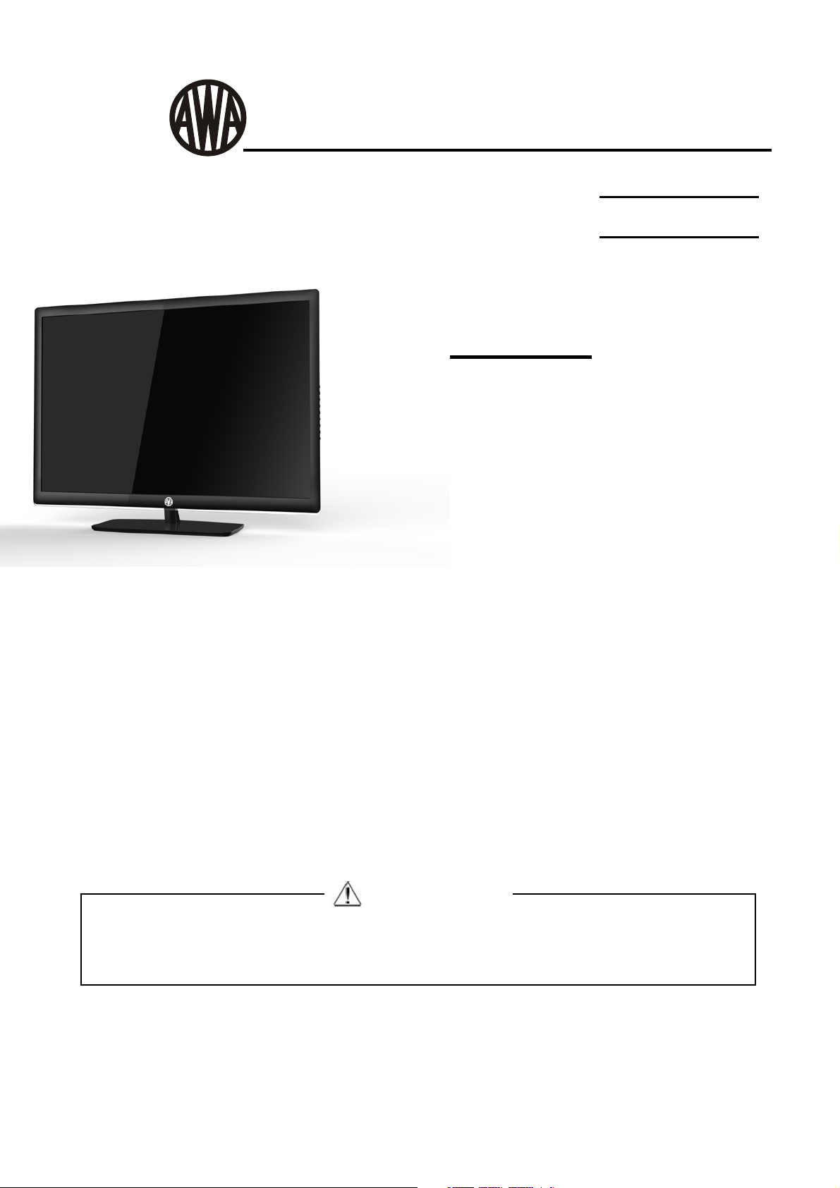
LED TV
Model No.
MSD306
MHDV2262-04
Chassis
WARNING
This service information is designed for experienced repair technicians only and is not designed for use by the general public.
It does not contain warnings or cautions to advise non-technical individuals of potential dangers in attempting to service a pr
Products powered by electricity should be serviced or repaired only by experienced professional technicians. Any attempt to
service or repair the product or products dealt with in this service information by anyone else could result in serious injury
oduct.
or death.
Page 2

Service Manual
Model No.:
Chapter 1: General Information
1-1. Table of Contents
1. General Information...........................................................................
1-1. Table of Contents
1-2. General Guidelines
1-3. Important Notice
1-4. How to Read this Service Manual
6SHFL¿FDWLRQV....................................................................................
3. Location of Controls and Components...........................................
3-1. Board Location
3-2. Main Board & AV Board
3-3. LCD Panel
4. Disassemble and Assemble..........................................................
4-1 Remove the Pedestal
4-2 Remove the Back Cover 12
4-3 Remove the Adhesive Tape 12
4-4 Remove the Main Board 13
10
12
12
1
1
3
3
6
6
8
8
8
8
4-5 Remove the Speaker 13
4-6 Remove the Remote Control Board 14
5. Installation Instructions..…....………………...........………….........
5-1 External Equipment Connections 15
5-2 HDMI Connections 18
6. Operation Instructions....…....………………...........………….........
6-1 Front Panel Controls
6-2 Back Panel Controls
6-3 Universal Remote Control
7. Electrical Parts…....………………...........………….........................
7-1. Circuit Diagram
7-2. Wiring Connection Diagram
15
21
21
21
22
23
23
33
- 01 -
Page 3

Service Manual
Model No.:
8. Measurements and Adjustments
8-1. How to enter into the factory model
8-2. How to update software
8-3. How to enter into the Hotel Model
........…………............................
9. Trouble-shooting…………..............................................................
9-1. Simple Check 46
9-2. Main Board Failure Check
9-3. Panel Failure
35
43
44
45
46
47
57
- 02 -
Page 4

Service Manual
Model No.:
1-2. General Guidelines
When servicing, observe the original lead dress. If a short circuit is found, replace all parts
which have been overheated or damaged by the short circuit.
After servicing, see to it that all the protective devices such as insulation barriers, insulation
papers shields are properly installed.
After servicing, make the following leakage current checks to prevent the customer from
being exposed to shock hazards.
1) Leakage Current Cold Check
2) Leakage Current Hot Check
3) Prevention of Electro Static Discharge (ESD) to Electrostatically Sensitive
1-3. Important Notice
1-3-1. Follow the regulations and warnings
Most important thing is to list up the potential hazard or risk for the service personnel to
open the units and disassemble the units. For example, we need to describe properly
how to avoid the possibility to get electrical shock from the live power supply or charged
electrical parts (even the power is off).
This symbol indicates that high voltage is present inside.It is dangerous to
make any king of contact with any inside part of this product.
This symbol indicates that there are important operating and maintenance
instructions in the literture accompanying the appliance.
1-3-2. Be careful to the electrical shock
7RSUHYHQWGDPDJHZKLFKPLJKWUHVXOW LQ HOHFWULFVKRFNRU¿UH
to rain or excessive moisture. This TV must not be exposed to dripping or splashing water,
DQGREMHFWV¿OOHGZLWKOLTXLGVXFKDVYDVHVPXVWQRWEHSODFHGRQWRSRIRUDERYHWKH79
GRQRWH[SRVHWKLV79VHW
1-3-3. Electro static discharge (ESD)
Some semiconductor (solid state) devices can be damaged easily by static electricity. Such
components commonly are called Electrostatically Sensitive (ES) Devices. The following
techniques should be used to help reduce the incidence of component damage caused by
electros static discharge (ESD).
1-3-4. About lead free solder (PbF)
This product is manufactured using lead-free solder as a part of a movement within the
consumer products industry at large to be environmentally responsible. Lead-free solder
must be used in the servicing and repairing of this product.
8VHWKHJHQHZLQJSDUWVVSHFL¿HGSDUWV
Special parts which have purposes of fire retardant (resistors), high-quality sound
(capacitors), low noise (resistors), etc. are used.
When replacing any of components, be sure to use only manufacture's specified parts
shown in the parts list.
Safety Component
Ɣ&RPSRQHQWVLGHQWL¿HGE\PDUNKDYHVSHFLDOFKDUDFWHULVWLFVLPSRUWDQWIRUVDIHW\
- 03 -
Page 5

1-3-6 Safety Check after Repairment
Service Manual
Model No.:
&RQ¿UPWKDWWKHVFUHZVSDUWVDQGZLULQJZKLFKZHUHUHPRYHGLQ
in the original positions, or whether there are the positions which are deteriorated around
the serviced places serviced or not. Check the insulation between the antenna terminal or
external metal and the AC cord plug blades. And be sure the safety of that.
RUGHUWRVHUYLFHDUHSXW
General Servicing Precautions
1. Always unplug the receiver AC power cord from the AC power source before;
a. Removing or reinstalling any component, circuit board module or any other receiver
assembly.
b. Disconnecting or reconnecting any receiver electrical plug or other electrical
connection.
c. Connecting a test substitute in parallel with an electrolytic capacitor in the receiver.
CAUTION: A wrong part substitution or incorrect polarity installation of electrolytic
capacitors may result in an explosion hazard.
2. Test high voltage only by measuring it with an appropriate high voltage meter or other
voltage measuring device (DVM, FETVOM, etc) equipped with a suitable high voltage
probe.
Do not test high voltage by "drawing an arc".
3. Do not spray chemicals on or near this receiver or any of its assemblies.
4. Unless specified otherwise in this service manual, clean electrical contacts only by
applying the following mixture to the contacts with a pipe cleaner, cotton-tipped stick or
comparable non-abrasive applicator; 10% (by volume) Acetone and 90% (by volume)
isopropyl alcohol (90%-99% strength).
CAUTION:7KLVLVDÀDPPDEOHPL[WXUH
8QOHVVVSHFL¿HGRWKHUZLVHLQWKLVVHUYLFHPDQXDOOXEULFDWL
Capacitors may result in an explosion hazard.
5. Do not defeat any plug/socket B+ voltage interlocks with which receivers covered by this
service manual might be equipped.
6. Do not apply AC power to this instrument and/or any of its electrical assemblies unless
all solid-state device heat sinks are correctly installed.
7. Always connect the test receiver ground lead to the receiver chassis ground before
connecting the test receiver positive lead.
Always remove the test receiver ground lead last. Capacitors may result in an explosion
hazard.
8VHZLWKWKLVUHFHLYHURQO\WKHWHVW¿[WXUHVVSHFL¿HGLQWKLVVHUYLFHPDQXDO
CAUTION: 'RQRWFRQQHFWWKHWHVW¿[WXUHJURXQGVWUDSWRDQ\KHDWVLQNLQWKLVUHFeiver.
9. Remove the antenna terminal on TV and turn on the TV.
RQRIFRQWDFWVLVQRWUHTXLUHG
10. Insulation resistance between the cord plug terminals and the eternal exposure metal
should be more than Mohm by using the 500V insulation resistance meter.
11. If the insulation resistance is less than M ohm, the inspection repair should be required.
If you have not the 500V insulation resistance meter, use a Tester. External exposure
metal: Antenna terminal Headphone jack
- 04 -
Page 6

Service Manual
Model No.:
Electrostatically Sensitive (ES) Devices
Some semiconductor (solid-state) devices can be damaged easily by static electricity.
Such components commonly are called Electrostatically Sensitive (ES) Devices.
Examples of typical ES devices are integrated circuits and some field-effect transistors
and semiconductor "chip" components. The following techniques should be used to help
reduce the ncidence of component damage caused by static by static electricity.
1. Immediately before handling any semiconductor component or semiconductorequipped assembly, drain off any electrostatic charge on your body by touching a known
earth ground. Alternatively, obtain and wear a commercially available discharging wrist
strap device, which should be removed to prevent potential shock reasons prior to applying
power to the unit under test.
2. After removing an electrical assembly equipped with ES devices, place the assembly
on a conductive surface such as aluminum foil, to prevent electrostatic charge buildup or
exposure of the assembly.
3. Use only a grounded-tip soldering iron to solder or unsolder ES devices.
4. Use only an anti-static type solder removal device. Some solder removal devices not
FODVVL¿HGDVDQWLVWDWLFFDQJHQHUDWHHOHFWULFDOFKDUJHVVXI¿
'RQRWXVHIUHRQSURSHOOHGFKHPLFDOV7KHVHFDQJHQHUDWHHO
to damage ES devices.
6. Do not remove a replacement ES device from its protective package until immediately
before you are ready to install it.
(Most replacement ES devices are packaged with leads electrically shorted together by
conductive foam, aluminum foil or comparable conductive material).
7. Immediately before removing the protective material from the leads of a replacement
ES device, touch the protective material to the chassis or circuit assembly into which the
device will be installed.
CAUTION:
safety precautions.
8. Minimize bodily motions when handling unpackaged replacement ES devices.
(Otherwise harmless motion such as the brushing together of your clothes fabric or the
OLIWLQJRI\RXUIRRWIURPDFDUSHWHGÀRRUFDQJHQHUDWHVWDWLFHOHFWULFLW\VXI¿FLHQWWRGDPDJH
an ES device.)
Be sure no power is applied to the chassis or circuit, and observe all other
FLHQWWRGDPDJH(6GHYLFHV
HFWULFDOFKDUJHVVXI¿FLHQW
1-3-7. Ordering Spare Parts
Please include the following informations when you order parts. (Particularly the Version
letter)
1. Model number, Serial number and Software Version
The model number and Serial number can be found on the back of each product and the
Software Version can be found at the Spare Parts List.
2. Spare Part No. and Description
<RXFDQ¿QGWKHPLQWKH6SDUH3DUWV/LVW
- 05 -
Page 7

1-3-8. Photo used in this manual
The illustration and photos used in this Manual may not base on the final design of
products, which may differ from your products in some way.
1-4. How to Read this Service Manual
Using Icons:
,FRQVDUHXVHGWRDWWUDFWWKHDWWHQWLRQRIWKHUHDGHUWRVSHFL¿FLQIRUPDWLRQ7KHPHDQLQJRI
each icon is described in the table below:
Note:
A “note” provides information that is not indispensable, but may nevertheless be valuable
to the reader, such as tips and tricks.
Service Manual
Model No.:
Caution:
A “caution” is used when there is danger that the reader, through incorrect manipulation,
may damage equipment, loose data, get an unexpected result or has to restart(part of) a
procedure.
Warning:
A “warning” is used when there is danger of personal injury.
Reference:
A “reference” guides the reader to other places in this binder or in this manual, where he/
VKHZLOO¿QGDGGLWLRQDOLQIRUPDWLRQRQDVSHFL¿FWRSLF
- 06 -
Page 8
Service Manual
Model No.:
6SHFL¿FDWLRQV
Model MHDV2262-04
Screen Size 21.5 inch
Aspect Ratio 16:9
Resolution 1920x1080
Response Time (ms)
5.0 (GRAY TO
GRAY)
Angel of View
160(H)/160(V)
Color Display 16.7M
No. of Preset Channels 1000
OSD Language English
Color System PAL/SECAM
Audio System
DK, BG, I, M, L, L'
Audio Output Power
3W×2
(Built-in) (W)
Audio Output Power
No
(outer) (W)
Total Power Input (W) 38W
Voltage Range (V)
Power Frequency (Hz)
AC 100-240V
50~60Hz
Net Weight (KG)
Gross Weight (KG)
Net Dimension (MM)
Packaged Dimension
(MM)
- 07 -
3.8
4.9
528*38*350
528*145*390
Page 9
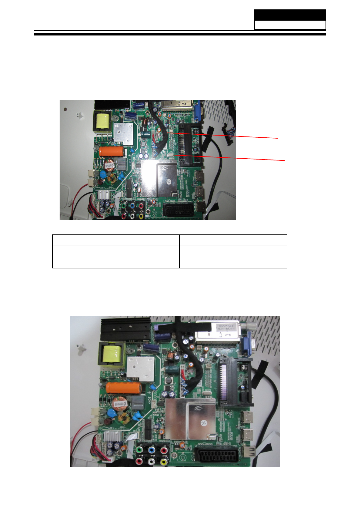
3. Location of Controls and Components
3-1 Board Location
Service Manual
Model No.:
B
A Board
No. Description
A Board Integration Mainboard
B
LVDS WIRE
3-2 Main Board
515C3212M21
4031C226209
- 08 -
Page 10
Service Manual
Model No.:
3-2-1 Function Description:
Main Board
Process signal which incept from exterior equipment then translate into signal that panel
can display.
&RQQHFWRUGH¿QLWLRQ
Main board connector
Keypad and remote connector (J28)
Pin number Signal name Description
1
2 LED_G
3
4
5
6
7
8
9
10
LED_R
STANDBY
IR REMOTE CONTROL
GND
5V
NC
KEY0
KEY1
GND
LAMP RED
LAMP GREEN
GND
POWER FOR REMOTE
Speaker connector (J26)
Pin number Signal name Description
1 RSPK+ RSPK+
2 RSPK- RSPK3 LSPK- LSPK4 LSPK+ LSPK+
- 09 -
Page 11
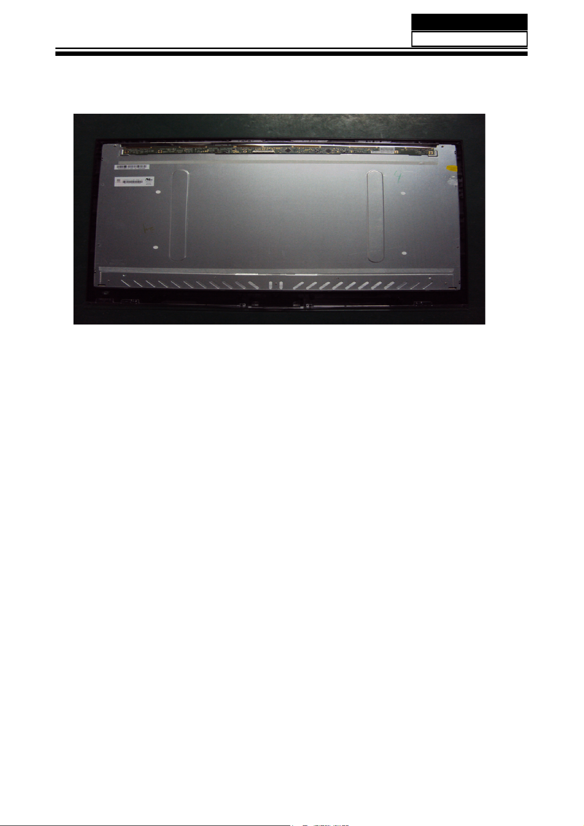
3-3. LED Panel
Service Manual
Model No.:
CLAA215FA10
- 10 -
Page 12

Service Manual
Model No.:
3-4-1.Connector de finition
PIN NO. REMARK FUNCTION
1 RXO0- minus signal of odd channel 0(LVDS)
2 RXO0+ plus signal of odd channel 0(LVDS)
3 RXO1- minus signal of odd channel 1(LVDS)
4 RXO1+ plus signal of odd channel 1(LVDS)
5 RXO2- minus signal of odd channel 2(LVDS)
6 RXO2+ plus signal of odd channel 2(LVDS)
7 GND GND
8 RXOC- minus signal of odd clock channel (LVDS)
9 RXOC+ plus signal of odd clock channel (LVDS)
10 RXO3- minus signal of odd channel 3(LVDS)
11 RXO3+ plus signal of odd channel 3(LVDS)
12 RXE0- minus signal of even channel 0(LVDS)
13 RXE0+ plus signal of even channel 0(LVDS)
14 GND GND
15 RXE1- minus signal of even channel 1(LVDS)
16 RXE1+ plus signal of even channel 1(LVDS)
17 GND GND
18 RXE2- minus signal of even channel 2(LVDS)
19 RXE2+ plus signal of even channel 2(LVDS)
20 RXEC- minus signal of even clock channel (LVDS)
21 RXEC+ plus signal of even clock channel (LVDS)
22 RXE3- minus signal of even channel 3(LVDS)
23 RXE3+ plus signal of even channel 3(LVDS)
24 GND GND
25 NC NC
26 NC Test pin (Can’t connect to GND)
27 NC NC
28 VCC Power supply input voltage(5.0 V)
29 VCC Power supply input voltage(5.0 V)
30 VCC Power supply input voltage(5.0 V)
1) Keep the NC Pin and don’t connect it to GND or other signals.
2) GND Pin must connect to the ground, don’t let it be a vacant pin.
- 11 -
Page 13
Service Manual
Model No.:
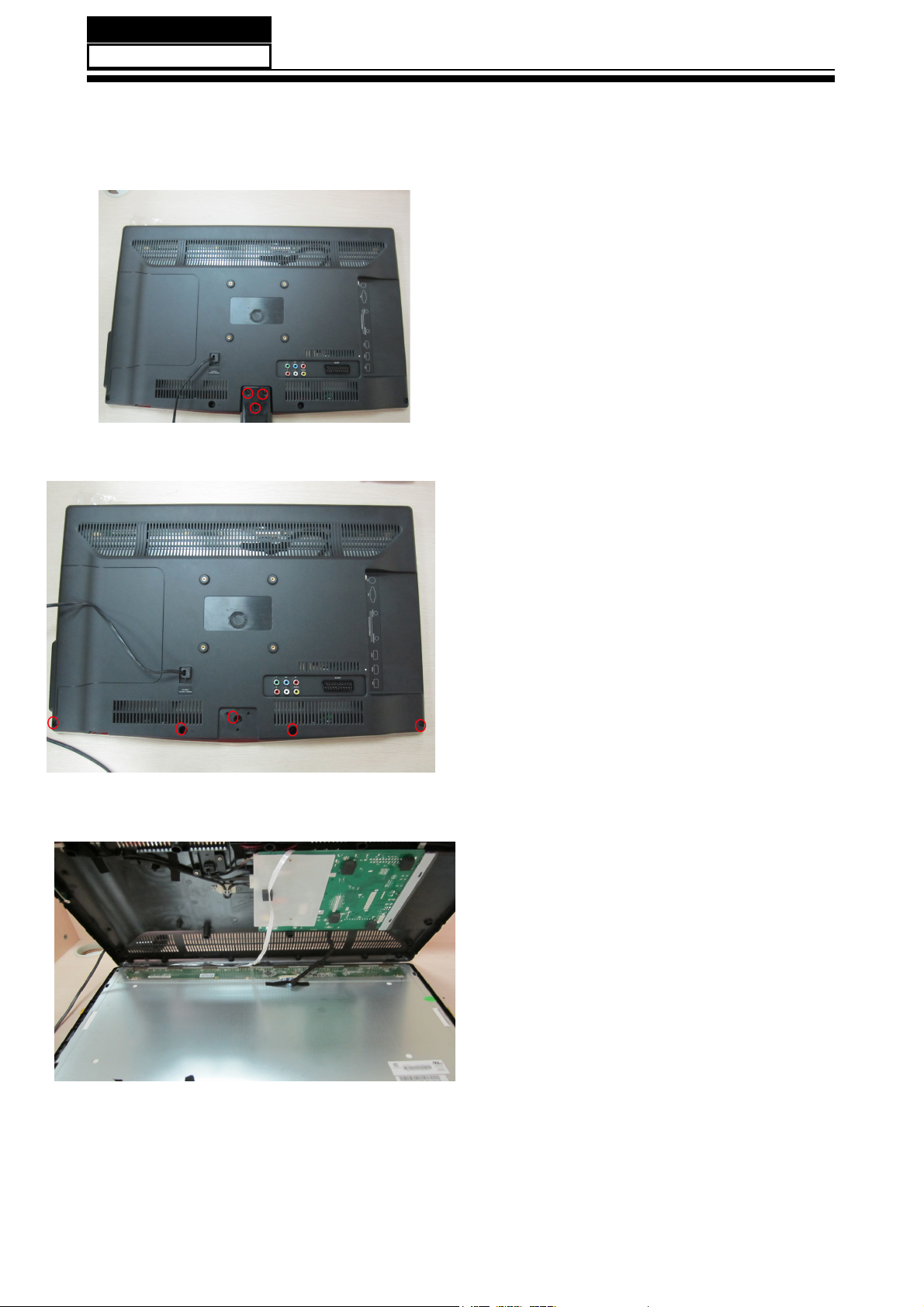
4. Disassemble and assemble
4-1 Remove the Pedestal
4-2Remove the Back Cover
/D\GRZQWKHXQLWVRWKDWUHDUFRYHU
faces upward
5HPRYH WKHWKUHH VFUHZIURPWKH
UHDUFRYHULQGLFDWHGZLWKż
7KHQUHPRYHWKHSHGHVWDO
4-3. Remove the adhesive tape
5HPRYHWKHWKHVHVFUHZLQGLFDWHGRQ
¿JXUHDERYHE\ż
7KHQUHPRYHWKH EDFNFRYHUIURP WKH
unit.
Remove the adhesive tape indicated on the
¿JXUHDERYH
- 12 -
Page 14
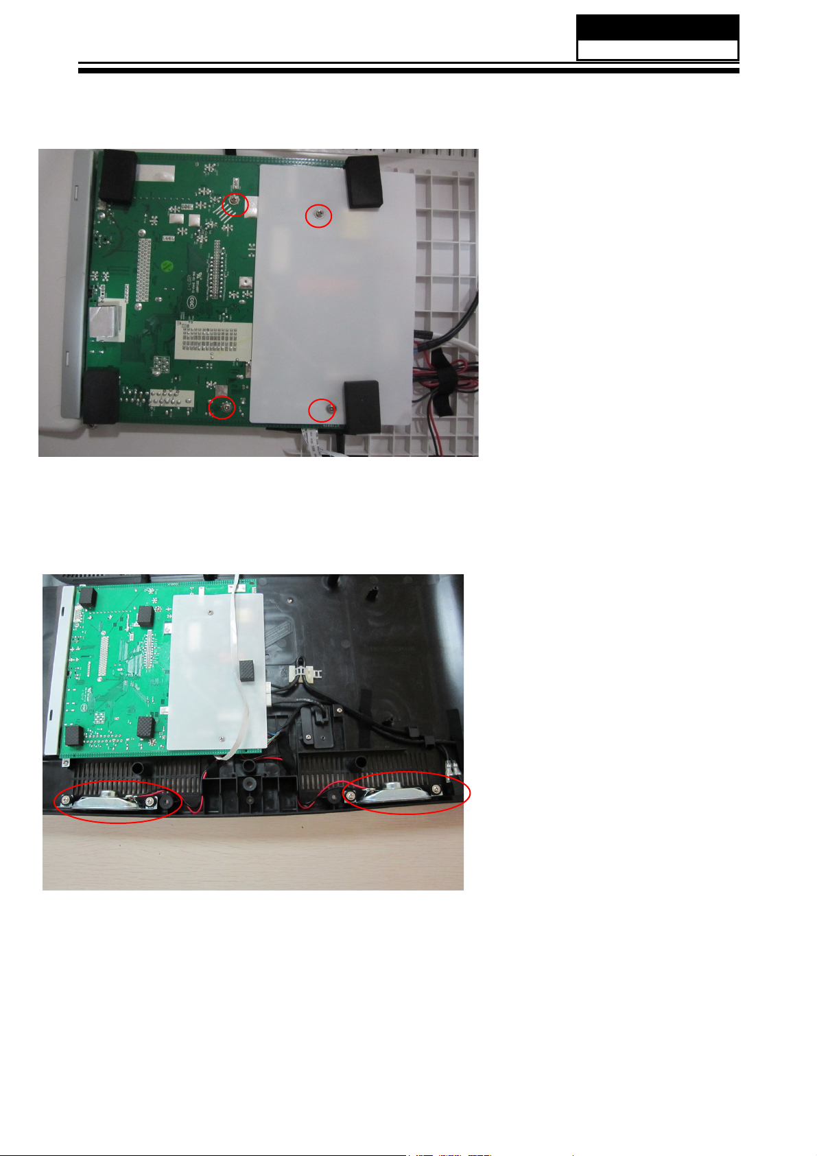
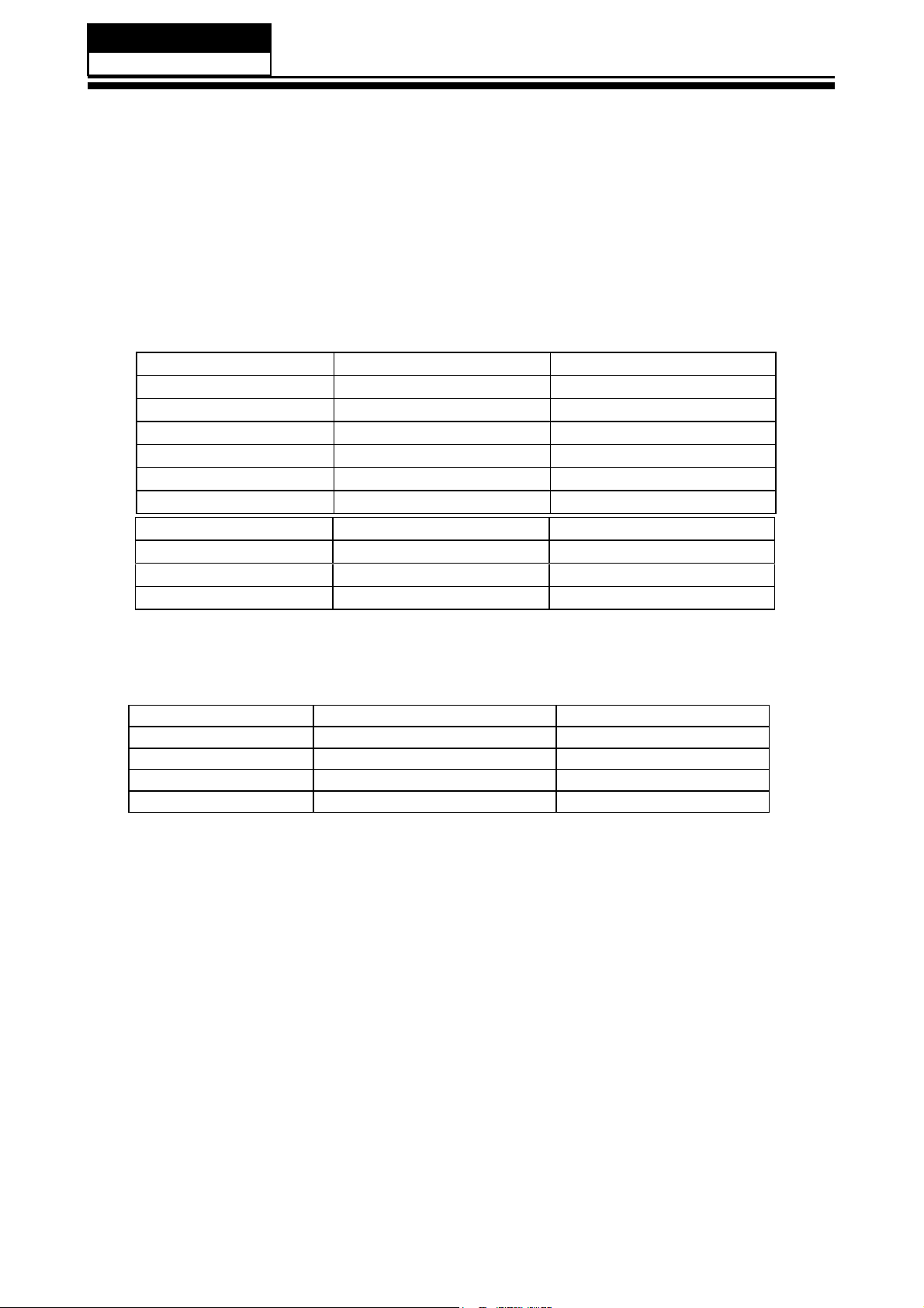
4-4 Remove the Main board
Service Manual
Model No.:
'LVFRQQHFWHG WKHFRXSOHU
J28
J26
J20
CN804
4-5 Remove the speaker
CN800
5HPRYHWKH0DLQERDUG
CN805
CN806
- 13 -
Take out the speaker
Page 15
Service Manual
Model No.:
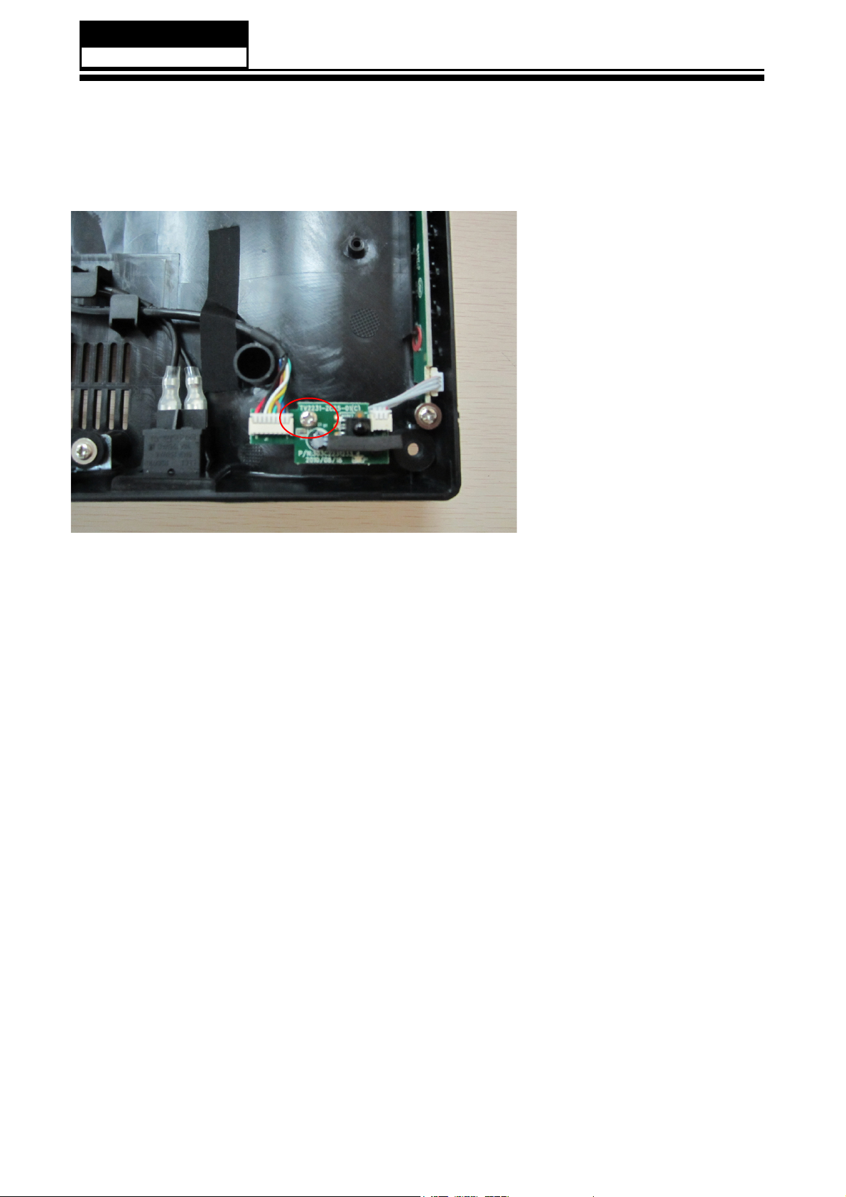
4-6 Remove the remote control
take out the remote control
board
- 14 -
Page 16
5. Installation Instructions
5-1 External Equipment Connections
Accessories
Service Manual
Model No.:
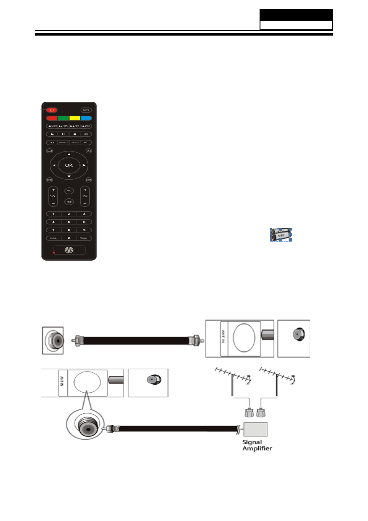
Remote Control
Antenna Connection
Connect one end of a coaxial cable (not included) to the ANT IN jack on the back of
your TV/DVD combo, then connect the other end of the cable into the antenna or cable
TV wall outlet.
User GUIDE
Battery
To improve picture quality from an antenna in a poor signal area, install a signal
DPSOL¿HU
If you need to split the antenna signal to connect two TVs, install a two-way splitter.
- 15 -
Page 17
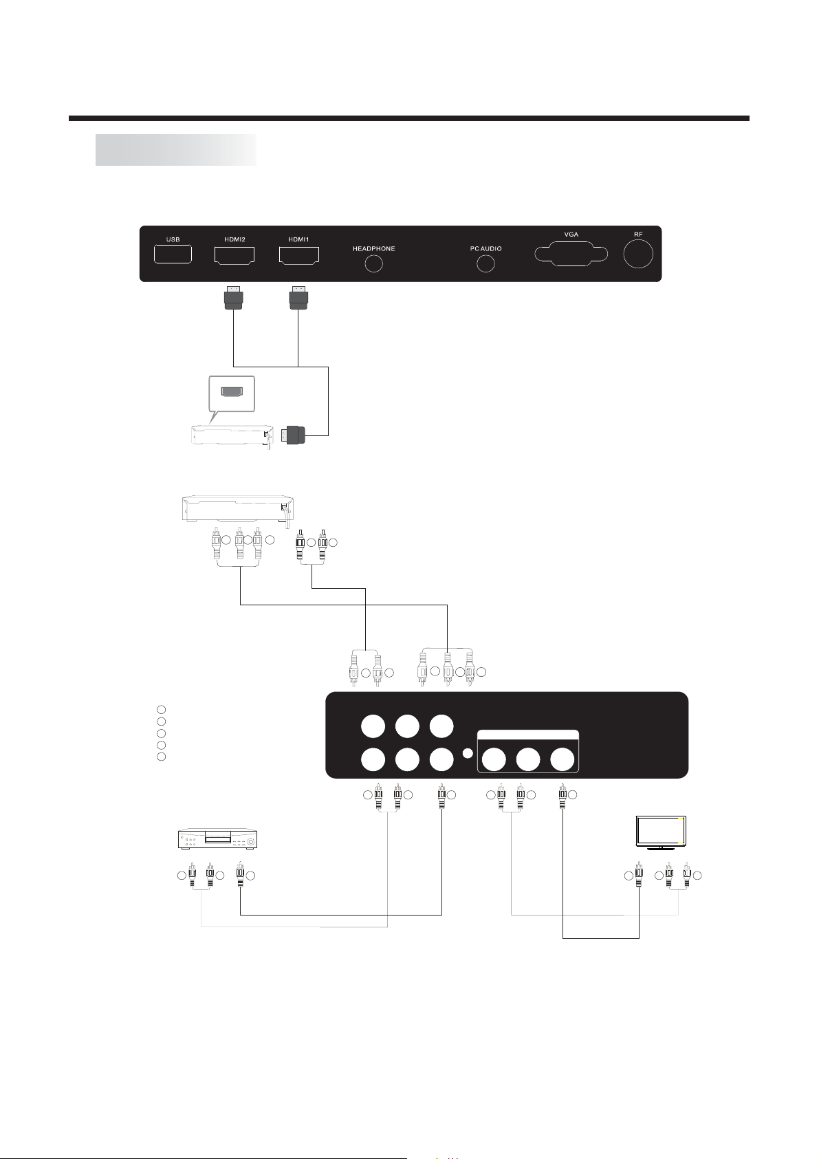
AV EQUIPMENT
You can use the input and output terminals on the TV set as follows.
- OR - N.B. Only one HDMI input can
be selected at a time.
HDMI
VIDEO EQUIPMENT with YPbPr output (Component video output)
INSTALLATION
G
B
Y
Yellow (Composite video)
W
White (audio L)
R
Red (audio R or Pr)
B
Blue (Pb)
G
Green (Y)
VIDEO EQUIPMENT (Composite video output)
VIDEO EQUIPMENT
W R
TO AUDIO OUTPUTS
Y
TO VIDEO
OUTPUT
R
W
R
Audio
G
VIDEO
R
W
YPbPr
RL
W R
R
B
Component video
AV OU T PUT
L
R
Y
W R
VIDEO
Y
TO VIDEO
INPUTS
VIDEO EQUIPMENT
W
Y
TO AUDIO INPUTS
R
Your TV can be connected to the following appliances: VCR, multi disc player, DVD, camcorder,
video game console or stereo system, etc.....
YPbPr (component video) can support these video formats: 480i, 576i, 480p, 576p, 720p.
Use an HDMI connection to view 1080i/1080p material.
- 16 -
Page 18
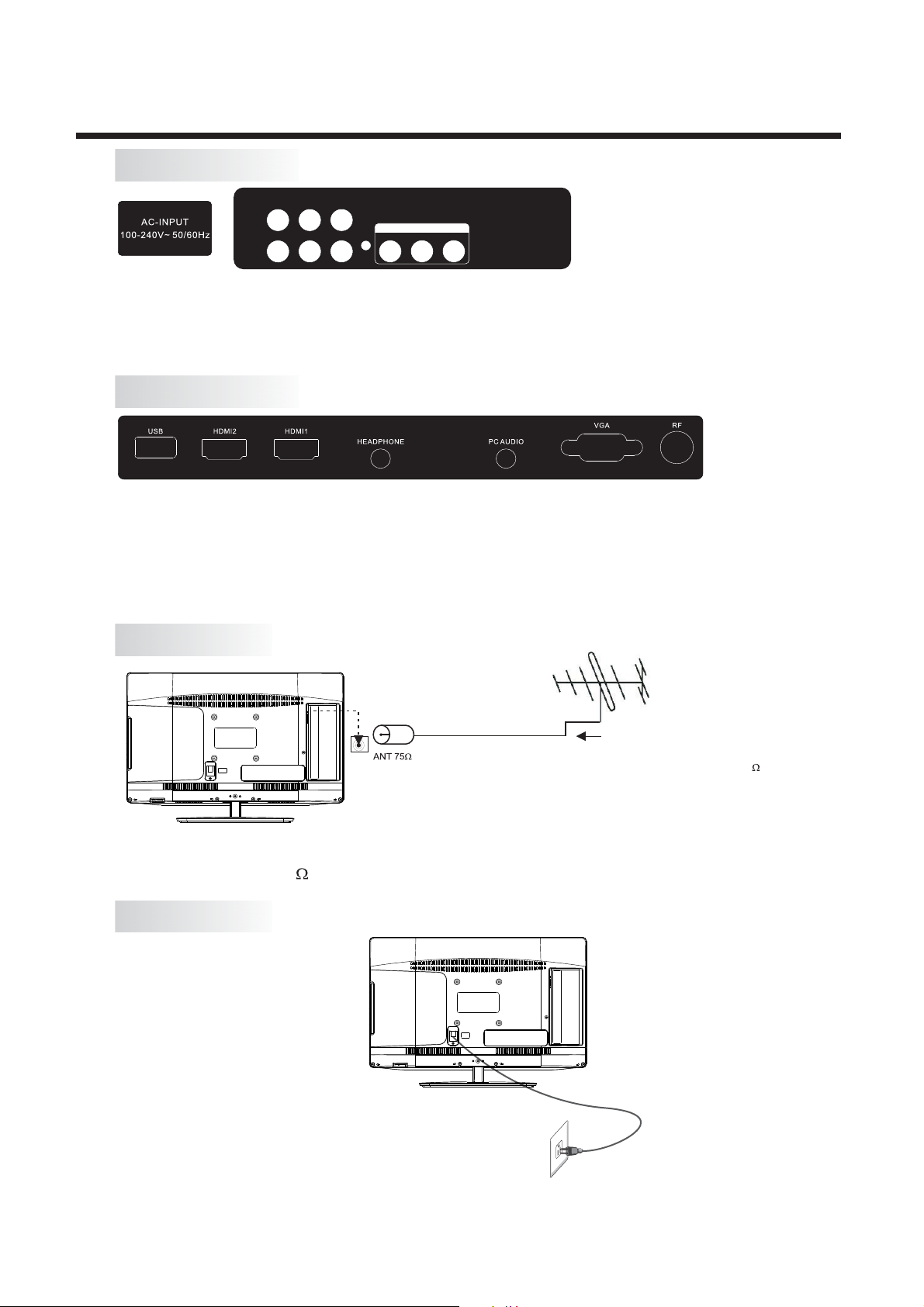
INSTALLATION
REAR AV Connections
YPbPr
RL
VIDEO
R
AV OUT P UT
L
VIDEO
All the terminals are (from left to right):
AC POWER INPUT, AV composite video
, (composite video and L+R audio).
input AV output
YPbPr (component video) inputs, L+R Audio inputs,
Note: 1. VIDEO and YPbPr share the same L+R audio inputs.
2. The AV output sockets are only functional during DVD operation.
SIDE AV Connections
All the terminals are (from left to right):
USB, HDMI2 input, HDMI1 input, HEADPHONE output, PC Audio input, VGA input,
Antenna socket.
Note: 1. When the HDMI1 input receives a DVI signal, the matching audio signal is received
by the PC Audio input.
2. When the HDMI2 port receives a DVI signal, the matching audio signal is received
by the YPbPr/AV Audio input.
ANTENNA
Plug (not supplied)
Note:
Aerial connections: IEC (PAL-type, female).
Input impedance: 75 unbalanced.
POWER
AC Input
100-240V~ 50/60Hz
Outdoor antenna (not supplied)
For optimum digital TV reception,
the use of high quality shielded 75
coax cable is recommended.
- 17 -
Page 19
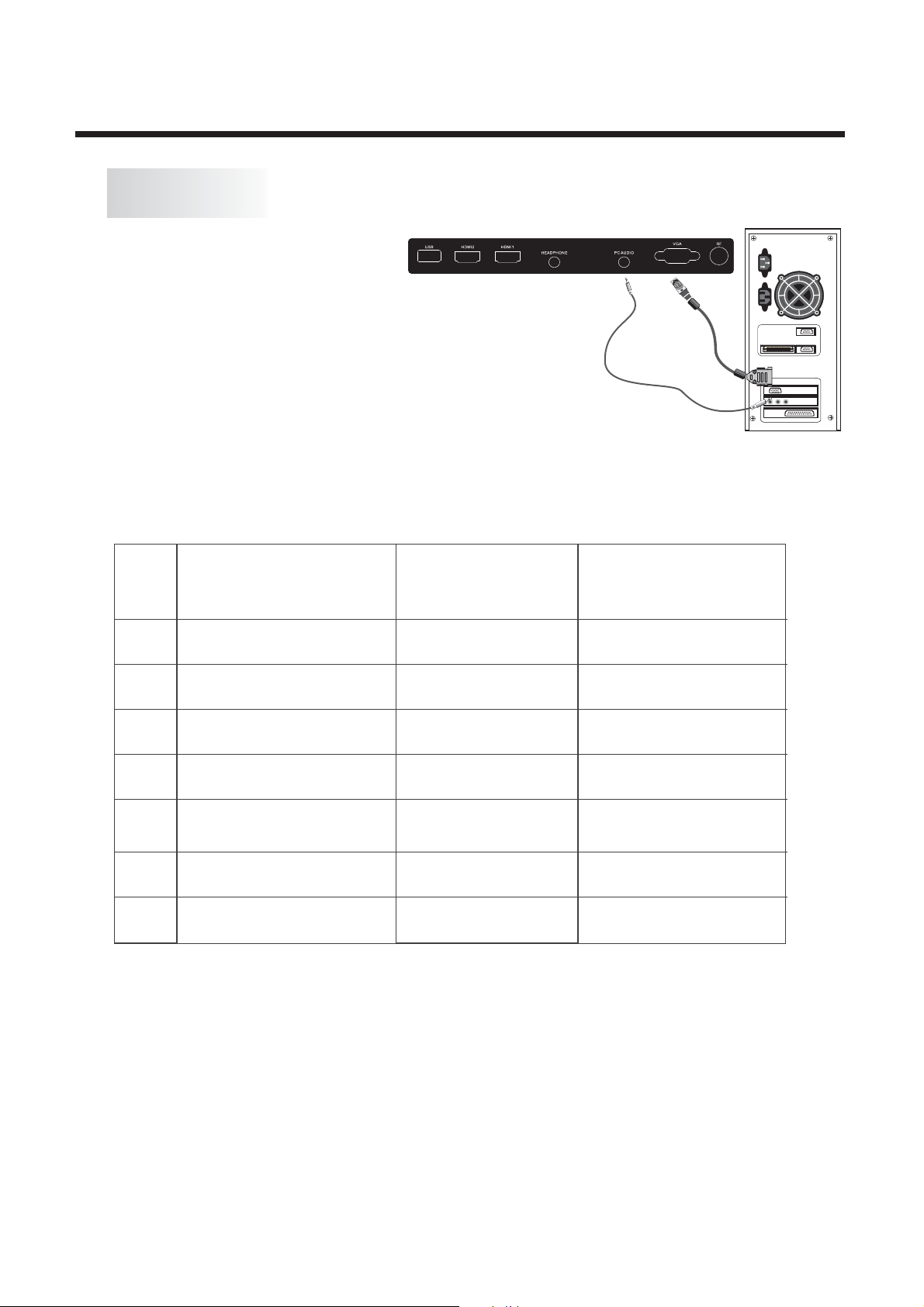
PC
STEPS:
Be sure both the TV and computer are set to Power off.
1.Connect a VGA and audio cable.
2.Connect the power cord.
3.Power on the TV, switch to PC mode.
4.Power on the PC.
This connection and power-up sequence is very
important.
PRESET MODE
VGA and audio cable
not supplied
INSTALLATION
RESOLUTION V.Freq.(Hz) H.Freq.(kHz)
1
2
3
4
5
6
7
The above resolutions are the only ones guaranteed to be supported. Other resolutions up to
1920 x 1080 may also be supported, but this must be assessed by the user on a case-by-case
basis. This is also subject to the limitiations of the computer’s video card.
720*400
640*480
800*600
800*600
800*600
1024*768
1024*768
70
60
56
60
72
60
70
31.47
31.47
35.156
37.88
48.08
48.36
56.48
- 18 -
Page 20

Service Manual
Model No.:
5-2 HDMI Connections
When the source device(DVD player or Set Top Box) supports HDM
How To Connect
1. Connect the source device to HDMI port of this TV with an HDMI cable(not supplied
with this product).
2. No separated audio connection is necessary.
How To Use
If the source device supports Auto HDMI function, the output resolution of the source
device will be automatically
set to 1280x720p.
If the source device does not support Auto HDMI, you need to set the output resolution
appropriately.
To get the best picture quality, adjust the output resolution of the source device to
1280x720p.
Select HDMI input source in input source option of Select Main source menu.
When the source device(DVD player or Set Top Box) supports DVI
How To Connect
1. Connect the source device to HDMI port of this TV with a HDMI-to-DVI cable(not
supplied with this product).
2. A separated audio connection is necessary.
3. If the source device has an analog audio output connector, connect the source device
audio output to DVI Audio In port located on the PC port.
How To Use
If the source device supports Auto DVI function, the output resolution of the source device
will be automatically
set to 1280x720p.
If the source device does not support Auto DVI, you need to set the output resolution
appropriately.
To get the best picture quality, adjust the output resolution of the source device to
1280x720p.
Press the INPUT button to select HDMI input source in input source option of Select Main
source menu.
Installation
- 18 -
Page 21

Cable sample
Service Manual
Model No.:
HDMI Cable
(not supplied with the product)
HDMI to DVI Cable
( not supplied with the product)
Analog Audio Cable
(Stereo to RCA type)
(not supplied with the product)
-19 -
Page 22

Service Manual
Model No.:
Power source
TO USE AC POWER SOURCE
Use the AC polarized line cord provided for operation on AC.
Insert the AC cord plug into a standard polarized AC outlet.
NOTES:
Ŷ1HYHUFRQQHFWWKH$&OLQHFRUGSOXJWRRWKHUWKDQWKHVSHFL¿HGYROWDJH
Use the attached power cord only.
Ŷ,IWKHSRODUL]HG$&FRUGGRHVQRW¿WLQWRDQRQSRODUL]HG
GRQRWDWWHPSWWR¿OHRUFXWWKHEODGH,WLVWKHXVHUCVUHVSRQ
electrician replace the obsolete outlet.
Ŷ ,I \RXFDXVH DVWDWLF GLVFKDUJHZKHQWRXFKLQJ WKHXQLW DQG
simply unplug the unit from the AC outlet and plug it back in. The unit should return to
normal operation.
$&RXWOHW
VLELOLW\WRKDYHDQ
WKHXQLW IDLOVWR IXQFWLRQ
- 20 -
Page 23

6. Operation Instructions
6-1 Front panel controls
Front panel
3
1
2
4
30 30
YPbPr
VGA
MTS
CC
DTV
HDMI
AV
TV
STRENGTH
CH LIST
CH LIST
EPG
FAV
TV
DISPLAY
S.M
CH
VOL
P.M
Service Manual
Service Manual
Model No.:
1: Remote control sensor.
2: Indicator LED:
BLUE = POWER ON.
RED = Stand-by.
3: Key board (on side of TV).
4: Main power switch (on bottom
panel of TV)
The remote control needs to be pointed directly,
within +/- 30 , of the senso r on the front of the
TV for reliable operation.
There will be a 5-10 second delay between
NB.
the power indicator LED changing state and the
TV responding.
KEYBOARD
SOURCE (Input selection)
MENU
CH+
CH-
VOL+
VOL-
STANDBY (Power ON/Stand-by select)
.:
1 SOURCE
Displays the input source Menu.
.:
MENU
2
Displays the main MENU.
.
3 CH+/CH-
In TV mode, press "CH+" or "CH-" to change the channel up or down.
In MENU mode, press "
.
VOL+/VOL-
4
Adjusts the sound level.
In MENU mode, adjust the item that you have selected.
5.
STANDBY
press "VOL+" or "VOL-" to
Once the TV's main power switch has been activated, press this button to turn the
unit ON from STANDBY mode.
Press it again to return the set back to STANDBY.
CH+" or "CH-" to select items.
- 21 -
Page 24

Service Manual
Model No.:
6-3 Setting Up Your Remote Control
REMOTE CONTROL
POWER
1: :To set the TV to standby or power on.
2: :In USB mode, used as reverse key, in teletext
1
2
3
4
5
6
7
8
9
10
11
12
13
14
VOL
FREEZE
CH
REC
mode used as subpage key.
16
3: : In USB mode, used as forword key, in teletext
mode used as reveal key.
4: :
Press the Play Button in USB Mode to begin or continue Playback.
5: :
17
18
19
20
21
22
23
Press the Pause Button to pause play in USB Mode.
6: :To enter or TELETEXT.
TEXT
7: : To turn on subtitles press the subtitle button in DTV mode.
SUBTITLE
8 : : Displays the main on-screen menu.
9 : : To move within the menu.
CURSOR
10: : Confirms selection.
OK
11: : To display information about the program being viewed
EPG
and what's on next in DTV mode.
12: : To access your favourite channels list in TV or DTV mode.
FAV
13: : To adjust sound level.
VOL+/-
14: : For direct access to channels.
NUMERIC KEY
15: : To select the available audio language of TV programs .
AUDIO
16: : To disable or enable the sound output.
MUTE
17: : In USB mode, used as next key, in teletext mode used as
list key.
24
18: : In USB mode, used as previous key, in teletext mode used
as hold key.
19: :In teletext mode used as index.
20: : Press to stop play in USB mode.
25
21: : To display the program information of the show you
INFO
are watching, press the info button.
22: Press to freeze the picture you are watching.
26
FREEZE:
23: : Press to display and select the available video sources.
24: : To return to the previous menu or exit menu.
EXIT
25: : To access the next or previous channels.
CH+/CH-
26: :
REC
DTV mode
27: : DTV Mode: RECALL: Jumps to last channel viewed.
RECALL
Press to record the TV program you are watching in
15
27
Remote Control Battery Installation
The remote control requires two AAA batteries. Below are steps to
assist you with replacing the batteries.
1.Open the back cover of the battery compartment.
2.Install the batteries into the battery tray. There are +/- polarity
markings in the battery compartment. Please ensure the battery
polarity is correct.
3.Close the battery cover.
Note:
There are two battery cov er typ es tha t may be u sed. P leas e
refer to picture 1 or picture 2 as applicable to the Remote Control
supplied with your TV.
Picture 1:
Picture 2:
- 22 -
Page 25

REMOTE CONTROL
TELETEXT
Teletext is an information system broadcast by certain channels which can be consulted like a newspaper. It also
offers access to subtitles for viewers with hearing problems or who are not familiar with the transmission language
(cable networks, satellite channels, etc.)
Press:
T
EXT
SELECTING A PAGE
DIRECT ACCESS
TO THE ITEMS
INDEX
SUB PAGE
HOLD
You will obtain:
This is used to call or exit teletext modes. The summary appears with a list of items that can be
accessed. Each item has a corresponding 3 digit page number. If the channel selected does
not broadcast teletext, the indication 100 will be displayed and the screen will remain blank (in
this case, exit teletext and select another channel).
Enter the number of the page required using the 0 to 9 up/down. Example: page 120, enter 120.
The number is displayed top left, the counter turns and then the page is displayed. Repeat this
operation to view another page. If the counter continues to search, this means that the page is
not transmitted. Select another number.
Coloured buttons correspond to the colours at the bottom of the screen. The 4 coloured keys
are used to access the items or corresponding pages. The coloured areas flash when the item
or the page is not yet available.
This returns to the contents page (usually page 100).
Certain pages contain sub-pages which are automatically displayed successively. This
key is used to stop or resume sub-page acquisition. The indication appears top left.
To freeze the page.
REVEAL
LIST
To display or hide the concealed information (games solutions).
The user can set four favourite pages to be directly linked to the four color keys. While list mode
is activated, it is not possibility to use TOP or FLOF navigation with the colourkeys. The
favourite page numbers should be stored and restored to/from nonvolatile memory for each
channel by the system software.
Page 26

4
7. Electrical parts
7-1.
D D
C C
B B
Circuit Diagram
5
RX3B0P
RX3B0N
RX3B1P
RX3B1N
RX3B2P
Page 5
RX3B2N
RX3BCLKP
RX3BCLKN
DDC3BSDA
DDC3BSCL
HOTPLUG3
RX2B0P
RX2B0N
RX2B1P
RX2B1N
RX2B2P
RX2B2N
RX2BCLKP
RX2BCLKN
DDC2BSDA
DDC2BSCL
HDMI_E_CEC
Page 3
03_AVIN&OUT
Page 4
04_HD&VGA
DVD-ON/OFF
Page 10
10_MST_POWER
HOTPLUG2
RGB0_RIN+
RGB0_RIN-
RGB0_GIN+
RGB0_GINRGB0_BIN+
RGB0_BINRGB0-SOG
SC1_FS
SC1_FB
AV1-Rin
VGA_AR
VGA_AL
SCART_AV
SIDE_AV
CVBS_OUT
AV1_AR
AV1_AL
PBINO+
PRINO+
REAR_AV
DVD_AV
ISP-RXD
ISP-TXD
DVD_AL
DVD_AR
05_HDMI
SC_ALOUT
SC_AROUT
YIN
PBIN
PRIN
PRIN
PBIN
YIN
PRIN
PBIN
YIN
AV1-Lin
IRIN
YINO+
SOY
RAIN+
GAIN+
BAIN+
SOG
VSYNC
HSYNC
HD1R
HD1L
ASEL0
4
RX3B0P
RX3B0N
RX3B1P
RX3B1N
RX3B2P
RX3B2N
RX3BCLKP
RX3BCLKN
DDC3BSDA
DDC3BSCL
HOTPLUG3
RX2B0P
RX2B0N
RX2B1P
RX2B1N
RX2B2P
RX2B2N
RX2BCLKP
RX2BCLKN
DDC2BSDA
DDC2BSCL
HOTPLUG2
HDMI_E_CEC
RGB0_RIN+
RGB0_RINRGB0_GIN+
RGB0_GINRGB0_BIN+
RGB0_BINRGB0-SOG
SC1_FS
SC1_FB
AV1-Rin
AV1-Lin
VGA_AR
VGA_AL
SCART_AV
SIDE_AV
CVBS_OUT
AV1_AR
AV1_AL
IRIN
YINO+
PBINO+
PRINO+
SOY
RAIN+
GAIN+
BAIN+
SOG
VSYNC
HSYNC
HD1R
HD1L
REAR_AV
DVD_AV
ASEL0
ISP-RXD
ISP-TXD
DVD-ON/OFF
DVD_AL
DVD_AR
Page 8
08_MSD306
3
MIUA_DQS0
MIUA_DQS0B
MIUA_DQS1
MIUA_DQS1B
MIUA_DQM1
MIUA_DQM0
MIUA_DQ[0:15]
MIUA_MCLK
MIUA_MCLKZ
MIUA_ODT
MIUA_WEZ
MIUA_MCKE
MIUA_BA1
MIUA_BA0
MIUA_A[0:12]
MIUA_BA2
MIUA_RASZ
MIUA_CASZ
OTG_DM
OTG_DP
ON_USB1
TSSTART
TSVALID
TSCLK
TS_MDI[7:0]
TS_MDO[7:0]
TS_MOCLK
TS_MOSTART
TS_MOVAL
PCM_D[7:0]
PCM_A[14:0]
PCM_IRQA_N
PCM_CE_N
PCM_IOWR_N
PCM_IORD_N
PCM_WE_N
PCM_OE_N
PCM_REG_N
PCM_WAIT_N
PCM_RESET
PCM_CD_N
CLASS_EN
AUOUTL1
AUOUTR1
AMP-Lout
AMP-Rout
HP_DET
POWERON/OFF
BKLON
ADJ-PWM
LCDON
RF_AGC_SELO
#IF_OUT
IF_OUT
IF_AGC
RF_AGC
VIFP
VIFM
T_SDA
T_SCL
2
MIUA_DQS0
MIUA_DQS0B
MIUA_DQS1
MIUA_DQS1B
MIUA_DQM1
MIUA_DQM0
MIUA_DQ[0:15]
MIUA_MCLK
MIUA_MCLKZ
MIUA_ODT
MIUA_WEZ
MIUA_MCKE
MIUA_BA1
MIUA_BA0
MIUA_A[0:12]
MIUA_BA2
MIUA_RASZ
MIUA_CASZ
OTG_DM
OTG_DP
ON_USB1
TSSTART
TSVALID
TSCLK
TS_MDI[7:0]
TS_MDO[7:0]
TS_MOCLK
TS_MOSTART
TS_MOVAL
PCM_D[7:0]
PCM_A[14:0]
PCM_IRQA_N
PCM_CE_N
PCM_IOWR_N
PCM_IORD_N
PCM_WE_N
PCM_OE_N
PCM_REG_N
PCM_WAIT_N
PCM_RESET
PCM_CD_N
CLASS_EN
AUOUTL1
AUOUTR1
AMP-Lout
AMP-Rout
HP_DET SC_AROUT
POWERON/OFF
BKLON
ADJ-PWM
LCDON
RF_AGC_SELO
#IF_OUT
IF_OUT
IF_AGC
RF_AGC
VIFP
VIFM
T_SDA
T_SCL
MIUA_DQS0
MIUA_DQS0B
MIUA_DQS1
MIUA_DQS1B
MIUA_DQM1
MIUA_DQM0
MIUA_DQ[0:15]
MIUA_MCLK
MIUA_MCLKZ
MIUA_ODT
MIUA_WEZ
MIUA_MCKE
MIUA_BA1
MIUA_BA0
MIUA_A[0:12]
MIUA_BA2
MIUA_RASZ
MIUA_CASZ
OTG_DM
OTG_DP
ON_USB1
TSSTART
TSVALID
TSCLK
TS_MDI[7:0]
TS_MDO[7:0]
TS_MOCLK
TS_MOSTART
TS_MOVAL
PCM_D[7:0]
PCM_A[14:0]
PCM_IRQA_N
PCM_CE_N
PCM_IOWR_N
PCM_IORD_N
PCM_WE_N
PCM_OE_N
PCM_REG_N
PCM_WAIT_N
PCM_RESET
PCM_CD_N
CLASS_EN
AUOUTL1
AUOUTR1
AMP-Lout
AMP-Rout
HP_DET
POWERON/OFF
BKLON
Page 2
ADJ-PWM
LCDON
02_SYS_POWER
RF_AGC_SELO
#IF_OUT
IF_OUT
IF_AGC
RF_AGC
VIFP
VIFM
T_SDA
T_SCL
Page 9
09_MEMORT
Page 7
07_PCMCIA
Page 11
11_AUDIO
Page 6
06_TUNER
SC_ALOUT
SC_AROUT
SC_ALOUT
1
A A
DESIGN:YANXUEWU
CHECKED: PART NO.: DWG NO.:
APPRD: SHEET: 1 OF 12 VER:1.0
5
4
3
2
MODEL: MSDV3205-L2 TITLE:TOP
SHEN ZHEN MTC MULTIMEDIA CO.,LTD
1
- 23 -
Page 27

5
4
3
2
1
MSD306 POWER SUPPLY
4
ADJ
OUT
ADJ
OUT
R269NCR269
IN
IN
U37靠近CA16
NC
U11
U11
AMS1117-3.3
AMS1117-3.3
D D
R2700RR270
0R
ADJ
OUT
ADJ
OUT
R271NCR271
NC
U12
U12
AMS1117-3.3
AMS1117-3.3
5VA
R2720RR272
+
C129
+
C129
0R
100uF/16V
100uF/16V
U13
U13
ADJ
OUT
ADJ
3.3VA
OUT
R2731kR273
1k
5VA
C135
C135
0.1u
0.1u
R2741KR274
1K
ADJ
OUT
ADJ
OUT
R275
R275
U14
U14
470R
470R
C149
C149
R276
R276
0.1u
0.1u
220R
220R
AMS1117-ADJ
AMS1117-ADJ
C C
AMS1117-ADJ
AMS1117-ADJ
B B
放置
321
3.3VU5Vstb
+
+
C126
C126
100uF/16V
100uF/16V
4
IN
IN
321
3.3VA
+
+
C131
C131
470uF/16V
470uF/16V
4
IN
IN
321
2.5VA
C136
C136
10uF
10uF
4
IN
IN
321
1.8VA
+
+
C150
C150
100uF/16V
100uF/16V
3.3VU
3.29V/380mA
C124
C124
C125
C125
0.1u
0.1u
NC/0.1u
NC/0.1u
3.29V/150mA
3.3VA
C127
C127
C128
C128
C130
C130
0.1u
0.1u
NC/0.1u
NC/0.1u
0.1u
0.1u
2.54V/230mA
2.5VA
C132
C132
C134
C134
C133
C133
NC/0.1u
NC/0.1u
NC/0.1u
NC/0.1u
0.1u
0.1u
1.8VA
1.84V/110mA
C137
C137
C138
C138
C139
C139
0.1u
0.1u
0.1u
0.1u
NC/0.1u
NC/0.1u
C306
C306
0.01u
0.01u
1.32V
1.31V/1100mA
C123
C121
C121
0.1u
0.1u
C307
C307
0.1u
0.1u
1.8VA
C140
C140
0.1u
0.1u
C123
C122
C122
0.1u
0.1u
0.1u
0.1u
230mA(DDR2/PCS)
C141
C141
C142
C142
C143
C143
C144
C144
C146
C146
C147
C147
C145
0.1u
0.1u
0.1u
0.1u
C145
0.1u
0.1u
0.1u
0.1u
0.1u
0.1u
0.1u
0.1u
0.1u
0.1u
C148
C148
0.1u
0.1u
+1.2V FOR MST CORE
TAB
U15
U15
AMS1117-ADJ
AMS1117-ADJ
V8ADJV8ADJV8ADJV8ADJ
8.12V
2
4
R279
R279
470R
470R
C152
C152
100uF/16V
100uF/16V
GND
C153
C153
0.1uF
0.1uF
GND
DESIGN:YANXUEWU
CHECKED: PART NO.: DWG NO.:
APPRD: SHEET: 10 OF 12 VER:1.0
MODEL: MSDV3205-L2 TITLE:MST_POWER
SHEN ZHEN MTC MULTIMEDIA CO.,LTD
2
1
+12V +8V
VIN3VOUT
C151
C151
Adjust
SOT223
SOT223
0.1uF
0.1uF
1
R277
R277
2.49K/%1
2.49K/%1
GND
3
+
C16510uF C16510uF
C163 470uF/16V+C163 470uF/16V
1.31V
C155
C155
0.1u
0.1u
0.1u
0.1u
C164 0.1uC164 0.1u
4
1.32V5VA
C158
C158
C157
C157
C156
C156
0.1u
0.1u
0.1u
0.1u
U16
U16
MP1482
MP1482
VCC2BS
100K
100K
7
R278
R278
C160
C160
10uF
10uF
A A
C161 0.1uC161 0.1u
EN
6
COMP
SW
8
SS
C159 1nFC159 1nF
R281
R281
C162 15nFC162 15nF
4
FB
AGND
6.8K
6.8K
5
1
3
5
C154
C154
15nF
15nF
R280 2KR280 2K
R282
R282
L80
L80
15H_2A
15H_2A
1.02A
1.27V
4.7K
4.7K
- 24 -
Page 28

5
4
3
2
1
+12V
PVCC
C169
C169
0.1uF
0.1uF
C173
C173
0.1uF
0.1uF
C236
C236
470uF/16V
470uF/16V
1 2
+
+
C241
C241
470uF/16V
470uF/16V
1 2
+
+
C243
C243
0.22uF
0.22uF
R380
R380
2R2
2R2
C244
C244
0.22uF
0.22uF
R381
R381
2R2
2R2
470uF/16V
470uF/16V
LOUT+
ROUT+
SVRR
C248
C248
+
+
LOUT#
LOUT#
ROUT#
R3782KR378
R3792KR379
2K
2K
R292 3KR292 3K
MUTEO
2N3904
2N3904
PVCC
L50
L50
FB_56OHM_500MA
FB_56OHM_500MA
L51NCL51
NC
L52
L52
FB_120_OHM_500MA
FB_120_OHM_500MA
R285 270KR285 270K
C176
C176
220uF/16V
220uF/16V
R301 220RR301 220R
D813 IN4148D813 IN4148
ROUT+
LOUT+LOUT+LOUT+LOUT+
SPEAKER
SPEAKER
1
2
3
4
J26
J26
C174
C174
10uF
10uF
3
Q26
Q26
2
R300 4.7KR300 4.7K
1
Q28
Q28
3906
3906
R306 10KR306 10K
C185
C185
PVCC
+5V
NC/1uF
NC/1uF
+
C167
+
C167
100uF/16V
100uF/16V
PVCC
C170
C170
C168
C168
0.1uF
0.1uF
0.001uF
0.001uF
PVCC
HP_RIN
1
VCC-OP2
C210
C210
0.1uF
0.1uF
R3391KR339
1K
3
Q33
Q33
2N3904
2N3904
2
R349
R349
330R
330R
Gain=R339/R349
+8V
R336
R336
10R
10R
220uF/16V
220uF/16V
C209 2.2uFC209 2.2uF
HP_LINP#
SVRR
LOUT#
C1103
C1103
+
+
C1104
C1104
1000pF
1000pF
C1101
C1101
R338
R338
330R
330R
CLASS_EN
C213
C213
R346
R346
10K
10K
HP_RINP#
0.1uF
0.1uF
1000pF
1000pF
3
Q32
Q32
1
2N3904
2N3904
2
MUTEO
ROUT#
HP_RINP#
U19
U19
TPA1517
TPA1517
1
20
IN1
GND/HS
2
19
SGND
GND/HS
3
18
SVRR
GND/HS
4
17
OUT1
GND/HS
5
16
PGND
GND/HS
6
15
OUT2
GND/HS
7
14
VCC
2K
8
M/SB
9
IN2
GND/HS10GND/HS
GND/HS
GND/HS
GND/HS
13
12
11
S1
1
2
10-2.54MMS110-2.54MM
R3762KR376
VCC-OP2
R3581KR358
1K
C222
HP_LIN
3
Q36
Q36
1
2N3904
2N3904
2
R364
R364
330R
330R
Gain=R358/R364
C222
2.2uF
2.2uF
CLASS_EN
C1102
C1102
R357
R357
330R
330R
R362
R362
10K
10K
HP_LINP#
0.1uF
0.1uF
1000pF
1000pF
C223
C223
3
Q35
Q35
1
2N3904
2N3904
2
Ground in the middle of the L/R
MUTE Control
R291
R302 10KR302 10K
R291
10K
10K
NC/10uF/16V/220uF/16V
NC/10uF/16V/220uF/16V
3
Q27
Q27
1
2N3904
2N3904
2
R3080RR308
0R
MUTEn
R299
R299
C180
C180
30K
30K
+
+
D D
CLASS_EN
CLASS_EN
AUDIO OP
HP_RINAMP-Rout
AMP-Rout
Location Near
IC Pin.
AMP-Lout
C C
AUOUTR1
AUOUTL1
B B
R313 100RR313 100R
200pF
200pF
AMP-Lout
R324 100RR324 100R
200pF
200pF
Location Near
IC Pin.
AUOUTR1
R340 100RR340 100R
AUOUTL1
R351
R351
C191
C191
C202
C202
200pF
200pF
100R
100R
200pF
200pF
R314
R314
100K
100K
HP_LIN
R325
R325
100K
100K
+8V
R3341KR334
1K
C212
C212
SC_AROUT
1uF
1uF
3
GAIN=1K/470R
Q31
Q31
1
2N3904
2N3904
R343
C216
C216
C221
C221
R343
2
100K
100K
330R
330R
R342
R342
+8V
R3481KR348
1K
3
Q34
Q34
C218
C218
1
2N3904
2N3904
2
100K
100K
R356
R356
R353
R353
330R
330R
SC_AROUT
RX56
RX56
NC/V800AA
NC/V800AA
SC_ALOUT
1uF
1uF
SC_ALOUT
RX57
RX57
NC/V800AA
NC/V800AA
HP_SL
HP_SMUTE
HP_SR
100uF/16V
100uF/16V
100uF/16V
100uF/16V
J6
GND
4
0
5
L
6
0
3
0
2
R
HeadphoneJ6Headphone
C299
C299
C300
C300
10UF
10UF
10UF
10UF
GND GND GND
10
1
2738495
GND
+5V
L97
L97
FB_56_OHM_4A
FB_56_OHM_4A
C301
C301
0.1uF
0.1uF
DESIGN:YANXUEWU
CHECKED: PART NO.: DWG NO.:
APPRD: SHEET: 11 OF 12 VER:1.0
MODEL: MSDV3205-L2 TITLE:AUDIO
SHEN ZHEN MTC MULTIMEDIA CO.,LTD
2
1
H1
1
HOLE
2
3
4
10-2.54MMH110-2.54MM
GND
A A
PH_Drive
HP_DET
HP_DET
HP_DET
HP_RIN
C295 2.2uFC295 2.2uF
+5V
HP_LIN
5
4
5VA
R315
R315
100K
100K
R321
R321
R322
R322
4.7K
4.7K
100R
C298
C298
0.1uF
0.1uF
100R
C204
C204
R3291KR329
1K
R3321KR332
C205
C205
1K
GND
U25
U25
1
8
OUTA
VDD
2
7
MUTE
OUTB
6
IN13BIAS
5
GND4IN2
DF3544
DF3544
GND
R416
R416
100K
100K
3
C200
C200
4.7uF
4.7uF
GND
R414
R414
100K
100K
R415
R415
100K
100K
GND
2.2uF
2.2uF
C302
C302
- 25 -
Page 29

5
C12
C12
0.1uF
0.1uF
5VSTB#
5.12V
5Vstb +5V
320mA
5.12V
D D
C C
B B
L57 FB_56_OHM_4AL57 FB_56_OHM_4A
5Vstb
C21
C21
C1097
C1097
10uF
10uF
0.1uF
0.1uF
D803
D803
D804
D804
2A06
2A06
2A06
D807
D807
2A06
D805
D805
2A06
2A06
2A06
2A06
34
LF801LF801
R876
R876
12
470K/1206
470K/1206
CX1CX1
R883
R883
R884
R884
R886
R886
RC1206
RC1206
2M/1206
2M/1206
RC1206
RC1206
R885
R885
2M/1206
2M/1206
RC1206
RC1206
NC/24K/0805
NC/24K/0805
2M/1206
2M/1206
R888
R888
RC1206
RC1206
2M/1206
2M/1206
102
102
102
102
CY800
CY800
CY801
CY801
34
LF800LF800
C1068
C1068
102/0805
102/0805
12
RV1
RV1
PTC
PTC
RDH5-3A-W
RDH5-3A-W
F800F800
1
2
1
2
CN800
CN800
CN805SWCN805
AC IN
AC IN
SW
+5V
PANEL POWER
C31nF C31nF
C2
+12V
12.21V
0.1uFC20.1uF
C9100pF C9100pF
C6
C7
C8
1nFC71nF
0.1uFC60.1uF
4.7nFC84.7nF
112mA
+5V
FB_56_OHM_4A
FB_56_OHM_4A
L56
L56
C19
C19
C1080
C1080
100pF
100pF
100pF
100pF
EC805
EC805
+
+
47uF/400V
47uF/400V
R877
R877
R878
R878
470k/1206
470k/1206
470k/1206
470k/1206
U807U807
5
3
RI
VDD
GATE
CS
2
FB
GND
1
1
U1U1
2
3
1
HS1HS1
2
3
C1072
C1072
C1079
C1079
C13
C13
0.1u
0.1u
10uF
10uF
47uF/50V
47uF/50V
C1056
C1056
6
4
5VA
0.1u
0.1u
TO INVERTER
BKLON
ADJ-PWM
R880
R880
C1053
C1053
10R/1206
10R/1206
+
+
ZC101
ZC101
27V
27V
104/50V/0805
104/50V/0805
2N3906
2N3906
R889
R889
Q811
Q811
100R/0603
100R/0603
R891
R891
1K/0805
1K/0805
R894
R894
470R/1206
470R/1206
C1069
C1069
101/0805
101/0805
LCDON
R10
R10
10K
10K
BKLON
BKLON
BKLON
BKLON
BKLON
BKLON
BKLON
ADJ-PWM
R865
R865
68K/2W
68K/2W
D809
D809
FR107
FR107
Q810
Q810
10N60
10N60
3
R890
R890
10K/0805
10K/0805
R892
R892
22R/0603
22R/0603
R895
R895
R896
R896
R897
R897
R7
10KR710K
C4 0.1uFC4 0.1uF
R8
Q2
100KR8100K
3
2N3904Q22N3904
LCDON
R9
1
4.7KR94.7K
2
R2251
R2251
4.7K
4.7K
+12V
+5V
+
+
C17
C17
100uF/16V
100uF/16V
3.3VA
+5V
R13
R13
R11
R11
R12
R12
10K
10K
10K
10K
10K
10K
32
Q3
R2298
R2298
1
32
Q4
4.7K
4.7K
1
R2299
R2299
2N3904Q32N3904
2N3904Q42N3904
4.7K
4.7K
R19 0RR19 0R
R211KR21
1K
C22
C22
0.1uF
0.1uF
R23NCR23
NC
T102
T102
T102
T102
D806
D806
T103
T103
T103
T103
EFD25
EFD25
EFD25
EFD25
3
10
3
10
1
NC
NP1
NP1
NP1
NP1
8
6
12V
12V
7
2
7
11
12V
2
12V
NC
C1034
C1034
472/1KV
472/1KV
NP2
NP2
NP2
NP2
NB2
NB2
NB2
NB2
1
12
6
8
5
9
D810
D810
HER207
HER207
4
FB7
40R
FB7
40R
2
100pF/1KVC1100pF/1KV
1
1R/1206
1R/1206
1R/1206
1R/1206
1R/1206
1R/1206
R867 22R/1206R867 22R/1206
R869 22R/1206R869 22R/1206
1
12
10
4
GND
6
GND
8
9
5
GND
GND
NP2
NP2
NP2
NP2
NB1
NB1
NB1
NB1
5
9
12
2
5V
5V
4
11
3
5V
5V
R882 22R/1206R882 22R/1206
R887 22R/1206R887 22R/1206
C1
R893
R893
470R-0603
470R-0603
5VSTB#
12
43
R898
R898
R899
R899
U808
U808
1K/0603
1K/0603
4.7K
4.7K
PC817
PC817
C1070
C1070
2.2uF
2.2uF
R9001KR900
1K
0.1uF(X7R)
0.1uF(X7R)
U809
U809
TL431
TL431
R902
R902
R901
R901
4.7K
4.7K
47K
47K
CY802
CY802
102
102
4
Q1 AO3407Q1 AO3407
32
1
C11
C11
C10NCC10
NC
0.01uF
0.01uF
R5 NCR5 NC
VCCLCDFN
R6 0RR6 0R
C1096
C1096
C1100
C1100
0.1uF
0.1uF
10uF
10uF
DC output R21 1K,C23 1uF for 3.3V
PWM output change DC power
BL_ONOUTPUT
BL-ADJUSTOUTPUT
C23
C23
2.2uF
2.2uF
Note: Left C23 NC, R21 change to 100ohm if
want to output PWM puls
+5V
+12V
TO-220B
TO-220B
SBR20100
SBR20100
C1022
C1022
L806
L806
680pF
680pF
1
1
2
2
10uH/3.8A
3
C1071
C1071
10uH/3.8A
3
+
+
+
+
C1037
C1037
680pF
680pF
470uF/16V
470uF/16V
C1039
C1039
C1081
C1081
1000uF/25V
1000uF/25V
1000uF/25V
1000uF/25V
POWERON/OFF
POWERON/OFF
SBR2060
SBR2060
TO-220B
TO-220B
D811
D811
1
1
2
2
3
L807
L807
3
680pF
680pF
10uH/3.8A
10uH/3.8A
+
+
C1065
C1065
C1058
C1058
470uF/16V
470uF/16V
C1064
C1064
2200uF/16V
2200uF/16V
3
VCCLCDVCCLCDFN
R832
R832
U3
100R
100R
LED2
LED4
NC/AP3608EU3NC/AP3608E
EN
VCC
AGND
SDBX
SDB
FB
ISET
FBX
NC
BL-ADJUSTOUTPUT
LED5
LED7
LED10
LED11
LED12
BL_ONOUTPUT
20
19
18
17
16
15
14
13
12
11
100R
100R
LED13
LED14
LED15
LED16
R850
R850
R835NCR835
NC
R837NCR837
NC
DB
SHD
R830
R830
20K
20K
R828
R828
BX
12K
12K
R76
R76
100R
100R
LED6
LED8
SHD+5V
U4
1
CH1
2
CH2
3
CH3
4
CH4
5
PGND1
6
PGND2
7
CH5
8
CH6
9
CH7
CH810PWM
R831
R831
51K
51K
NC/AP3608EU4NC/AP3608E
FB
R829NCR829
NC
+5V
C15
C15
C18
C18
0.1uF(X7R)
0.1uF(X7R)
1uF
1uF
BL_ONOUTPUT
+12V
C14
C14
105/25V/0603
105/25V/0603
20
EN
19
VCC
18
AGND
17
SDBX
16
SDB
15
FB
14
ISET
13
FBX
12
NC
11
BL-ADJUSTOUTPUT
+12V
R720
R720
20K/0402
20K/0402
R721
R721
10K/0402
10K/0402
U5
1
UVLO
OVP
2
OV
R14
R14
3
EN
AP3039AU5AP3039A
100R
100R
4
VIN
5
VCC
DRV
6
OUT
7
PGND
C27
C27
105/25V/0603
105/25V/0603
CN804
CN804
LED1
1
LED2
2
LED3
3
LED4
4
5
LED+
6
LED+
7
8
LED5
9
LED6
10
LED7
11
LED8
12
NC/HEADER 12
NC/HEADER 12
R838
R838
100R
100R
BL_ONOUTPUTLED9
+5V
DB
C16 1uF-0603C16 1uF-0603
0.1uF(X7R)
0.1uF(X7R)
C20
C20
BX
R841
R841
R842NCR842
12K
12K
NC
R77
R77
100R
100R
NC
R848NCR848
LED9
LED10
R849NCR849
LED13
LED14
NC
L805
L805
10525V/0603
10525V/0603
10uH/3A
10uH/3A
+
+
C38
C38
C1021
C1021
47uF/50V
47uF/50V
LED1
LED2
LED3
COMP
SHDN
AGND
104/25V/0805
104/25V/0805
SS
CS
270K/0603
270K/0603
LED4
LED+
LED5
LED6
LED7
LED8
14
13
12
FB
11
10
9
8
RT
R18
R18
BL-ADJUSTOUTPUT
LED11
LED15
C31
C31
R847NCR847
NC
DRV
C34
C34
FB
SHD
102/25V/0805
102/25V/0805
CN803
CN803
1
2
3
4
5
6
7
8
9
10
NC/FOR CPT
NC/FOR CPT
R846NCR846
NC
Q103
Q103
B601001
B601001
R700
R700
TO252-DPAK
TO252-DPAK
22R/0805
22R/0805
R2297
R2297
10K/0805
10K/0805
C35NCC35
NC
R839
R839
3.9K
3.9K
R65 1R/0805R65 1R/0805
R68 1R/0805R68 1R/0805
C32
C32
R69 1R/0805R69 1R/0805
101/25V/0402
101/25V/0402
103/25V/0805
103/25V/0805
CN802
CN802
LED1
1
LED2
2
LED3
3
LED4
4
LED+
5
6
LED5
7
LED6
8
LED7
9
LED8
10
NC/FOR CPT
NC/FOR CPT
R843
R843
R845
R845
FB
510K
510K
R844
R844
200K
200K
LED12
LED16
LED1
1
CH1
LED2
2
CH2
LED3
3
CH3
LED4
4
CH4
5
PGND1
6
PGND2
LED5
7
CH5
LED6
8
CH6
LED7
9
CH7
LED8
CH810PWM
NC
R834NCR834
LED1
R836NCR836
LED3
NC
J4
J8
1
2
CON2J8CON2
J3
1
2
CON2J3CON2
C1038
C1038
0.1uF-0603
0.1uF-0603
+12VB
+
+
C1035
C1035
H:ON
R875
R875
L:OFF
10k
10k
PSON
C10511nC1051
+
+
C1059
C1059
0.1uF(X7R)
0.1uF(X7R)
1n
CON4J4CON4
l
老化端口
C1040
C1040
0.1uF-0603
0.1uF-0603
R858
R858
10K
10K
POWERON/OFF#
5VSTB#
100pF
100pF
C1060
C1060
13V
13V
ZD102
ZD102
J7
1
2
5VSTB#
1
3
2
4
PSON
CON2J7CON2
Q806
Q806
B601001
B601001
TO252-DPAK
TO252-DPAK
C1041
C1041
+12V
0.1uF/25V/0805
0.1uF/25V/0805
+12V
EC806
EC806
+
+
220uF/16V
220uF/16V
R870
R870
100K
100K
Q808
Q808
2N3904
2N3904
R874
R874
100K
100K
Q809
Q809
+5V
AO4468
AO4468
5VSTB#
138
+5V
7
2
6
4
5
C1063
C1063
+
C1066
+
C1066
0.1uF(X7R)
0.1uF(X7R)
220uF/16V
220uF/16V
C1061
C1061
0.1uF(X7R)
0.1uF(X7R)
+12V
12V
稳压电路
POWERON/OFF#
10K
10K
R2307
R2307
Q812
Q812
3904
3904
10K
10K
R2308
R2308
OVP
101/25V/00603
101/25V/00603
R750
R750
FB1
47R/0402
47R/0402
C750
C750
FB1
20K
20K
用于
18.5和21.6 U3 U4
1 CN2
2 CN805 CN806 用于26",CN2
3 CN804 用于23.6, U4
NC/SS36
NC/SS36
D10
D10
2 1
D9
2 1
SS36D9SS36
C37
C37
R8561RR856
1R
LED
不插。
不贴。
2
LED+
R823
R823
51K
51K
C1026
C1026
+
+
C931
C931
0.1u/50V/0805
0.1u/50V/0805
220uF/50V
220uF/50V
+
C5NC+
C5
NC
R826
R826
1.5K
1.5K
CN2
CN2
LED+
3
1
3
1
4
2
4
2
HEADER 2
HEADER 2
R8601RR860
1R
J2
LED1
1
LED3
2
3
LED+
4
LED5
5
LED7
6
NC/FOR CPTJ2NC/FOR CPT
CN806
CN806
LED9
1
LED10
2
LED11
3
LED12
4
5
LED+
6
LED+
7
8
LED13
9
LED14
10
LED15
11
LED16
12
NC/HEADER 12
NC/HEADER 12
不贴。
D10
不插
A A
MODEL: MSDV3205-L2 TITLE:SYS_POWER
DESIGN:YANXUEWU
CHECKED: PART NO.: DWG NO.:
APPRD: SHEET: 2 OF 12 VER:1.0
5
4
3
2
1
SHEN ZHEN MTC MULTIMEDIA CO.,LTD
- 26 -
Page 30

5
4
3
2
1
SCART
SC1_FB
SC1_FS
SC1_FSO
0-2v: TV Mode
5-8v: 16:9 AV
9.5-12v: 4:3 AV
RX5
RX5
RX6
RX6
NC/V800AA
NC/V800AA
SC1_FB
SC_ALOUT
SC_AROUT
C1074
C1074
C1075
C1075
1000pF
1000pF
1000pF
1000pF
AGND AGND
R:10ohm,C:1uF 47nF Location near MST.IC
R37 0RR37 0R
R38 33RR38 33R
R39 33RR39 33R
R40 33RR40 33R
RX7
RX7
R44 68RR44 68R
R45 68RR45 68R
NC/V800AA
NC/V800AA
R46 68RR46 68R
SC_ALOUT
SC_AROUT
C1078 1nC1078 1n
C39 47nC39 47n
C40 47nC40 47n
C41 47nC41 47n
C42 47nC42 47n
C43 47nC43 47n
C44 47nC44 47n
RGB0-SOG
RGB0_GIN+
RGB0_BIN+
RGB0_RIN+
RGB0_BINRGB0_GINRGB0_RIN-
CVBS_OUT
RX1
RX1
R25
NC/V800AA
NC/V800AA
R25
75R
75R
10K
10K
RX4
RX4
R30
R30
R33
R33
NC/V800AA
NC/V800AA
2.2K
2.2K
Y
Pb
Pr
R4275R R4275R
R4375R R4375R
R41
R41
75R
75R
NC/V800AA
NC/V800AA
P1
21
AV1-V
20
VOUT
19
18
17
16
Pr
D D
C C
15
14
13
12
Y
11
10
9
SC1_FSO
8
7
6
5
4
3
2
1
24
25
SCARTP1SCART
Pb
AV1-L
SC_ALOUT
AV1-R
SC_AROUT
SC1_FSO
L58
L58
FB_11_OHM_500MA
FB_11_OHM_500MA
AV1-V
RX2
RX2
NC/V800AA
NC/V800AA
Keep AGND trace with signal
Keep spacing for L/R
AV1-L
AV1-R
RGB0-SOG
RGB0_GIN+
RGB0_BIN+
RGB0_RIN+
RGB0_BINRGB0_GINRGB0_RIN-
CVBS_OUT
SIDE CVBS Input
R:10ohm,C:1uF 47nF Location near MST.IC
R24 33RR24 33R
C1073
C1073
R26
R26
75R
75R
100p
100p
R:10ohm,C:1uF 47nF Location near MST.IC
R31 10KR31 10K
R35 10KR35 10K
C45
C45
4.7uF/1206
4.7uF/1206
C33 1uFC33 1uF
R34
R34
C1076
C1076
10K
10K
100p
100p
C36 1uFC36 1uF
C1077
C1077
R36
R36
100p
100p
10K
10K
+8V
AV Output
R48
R48
R47
R47
330R
330R
22K
22K
1
32
3906Q83906
Q9
Q8
2N3904Q92N3904
1
R49
R49
R51
R51
10K
10K
75R
75R
R52
R52
75R
75R
AGND
C26 47nC26 47n
3 2
R50
R50
AV1-Lin
AV1-Rin
75R
75R
SCART_AV
AV1-Lin
AV1-Rin
SCART_AV
VOUT
RX8
RX8
C47
C47
NC/V800AA
NC/V800AA
100pF
100pF
J32
J32
NC/AV-JACK-3/AVOUT
NC/AV-JACK-3/AVOUT
1
1
2
2
3
3
4
4
5
5
6
6
7
8
7
8
VGA_ARI
VGA_ALI
VOUT
SC_ALOUT
SC_AROUT
R53 10KR53 10K
R54 10KR54 10K
R55 10KR55 10K
C49
SIDE_AURIN
SIDE_AVIN
SIDE_AULIN
5
C49
100pF
100pF
C50
C50
100pF
100pF
RX9
RX9
R59 10KR59 10K
FB_11_OHM_500MA
FB_11_OHM_500MA
NC/V800AA
NC/V800AA
R56
R56
10K
10K
R:10ohm,C:1uF 47nF Location near MST.IC
R60
R60
10K
10K
L60
L60
C57
C57
100pF
100pF
C56 47nC56 47n
R61
R61
47R
47R
R62
R62
75R
75R
B B
A A
AV1_AL
AV1_AR
SIDE_AV
4
AV1_AL
AV1_AR
C48 1uFC48 1uF
C53 1uFC53 1uF
Keep AGND trace with signal
Keep spacing for L/R
Keep trace width(12mil+)
SIDE_AV
PC Audio Input
PC Audio Input
CN14 YPbPr-JACK-3CN14 YPbPr-JACK-3
7
8
7
8
3
7
8
J5
J5
1
4
5
2
3
6
1
1
2
2
3
3
4
4
5
5
6
6
CN807 AV-JACK-3CN807 AV-JACK-3
YIN SIDE_AVIN
YIN
PBIN
PBIN
PRIN
PRIN
8
8
C51
C51
VGA_ALI
R57 10KR57 10K
R58 10KR58 10K
C54
C54
C55
C55
100pF
100pF
100pF
100pF
1
1
2
2
3
3
4
4
5
5
6
6
7
7
VGA_AL
VGA_ARI
SIDE_AULIN
SIDE_AURIN
C52 1uFC52 1uF
2
VGA_AL
VGA_AR
1uF
1uF
VGA_AR
C:1uF Location near MST.IC
Keep AGND trace with signal
Keep spacing for L/R
Keep trace width(12mil+)
DESIGN:YANXUEWU
CHECKED: PART NO.: DWG NO.:
APPRD: SHEET: 3 OF 12 VER:1.0
MODEL: MSDV3205-L2 TITLE:AVIN&OUT
SHEN ZHEN MTC MULTIMEDIA CO.,LTD
1
- 27 -
Page 31

5
4
3
2
1
AV1/YPbPr/DVD INPUT
YIN
PBIN
PRIN
D D
J10
J10
CON4
CON4
4
4
3
3
2
2
1
1
C C
CON7
CON7
YIN
YIN
YIN
YIN
YIN
YIN
YIN
YIN
YIN
YIN
YIN
YIN
YIN
YIN
YIN
YIN
YIN
YIN
PBIN
PBIN
PBIN
PBIN
PRIN
C66
C66
33pF
33pF
+5V
C902
C902
C901
C901
100pF
J11
J11
100pF
100pF
100pF
1
1
2
2
3
3
DVD_AVIN
4
4
5
5
6
6
7
7
C6833pF C6833pF
C67
C67
RX10NC/V800AA RX10NC/V800AA
33pF
33pF
R79 100RR79 100R
R80 100RR80 100R
R82 100RR82 100R
R83 10RR83 10R
L61
L61
FB_11_OHM_500MA
FB_11_OHM_500MA
L62
L62
FB_11_OHM_500MA
FB_11_OHM_500MA
L63
L63
FB_11_OHM_500MA
FB_11_OHM_500MA
RX11
RX11
RX12
RX12
NC/V800AA
NC/V800AA
NC/V800AA
NC/V800AA
R2303 NCR2303 NC
R78 NCR78 NC
C74 1uFC74 1uF
C75 1uFC75 1uF
DVD-ON/OFF
IRIN
R71
R71
75R
75R
DVD_AL
R72
R72
75R
75R
DVD_AVIN
DVD_AR
YINO
PBINO
PRINO
R73
R73
75R
75R
L66
L66
FB_11_OHM_500MA
FB_11_OHM_500MA
DVD_AR
DVD_AL
DVD-ON/OFF
IRIN
R & C Location near MST.IC
C76
C76
100pF
100pF
YINO
PBINO
PRINO
R66 33RR66 33R
R2300 33RR2300 33R
R2301 33RR2301 33R
R70 0RR70 0R
C73 47nC73 47nR2302
R2302
47R
47R
R81
R81
75R
75R
C60 47nFC60 47nF
C63 47nFC63 47nF
C64 47nFC64 47nF
C65 1nFC65 1nF
DVD_AV
YINO+
PBINO+
PRINO+
SOY
DVD_AV
YINO+
PBINO+
PRINO+
SOY
VGA INPUT
GSCLGSCL
RX15NC/V800AA RX15NC/V800AA
RX14
RX14
B B
1617
J12
J12
15
5
10
14
4
9
13
3
8
12
2
7
11
1
PC_DB15HD_MIDDLE
PC_DB15HD_MIDDLE
6
IVS
IVS
IVS
IVS
IVS
IVS
IVS
IVS
IVS
IVS
IVS
IVS
IVS
IVS
IVS
IVS
IVS
IVS
IHS
GBLUGBLUGBLUGBLUGBLUGBLU
GGRN
GGRN
GGRN
GGRN
GGRN
GGRN
GRED
GRED
GRED
GRED
GRED
GRED
RX16NC/V800AARX16NC/V800AA
RX17NC/V800AARX17NC/V800AA
RX18NC/V800AARX18NC/V800AA
RX19NC/V800AARX19NC/V800AA
RX20NC/V800AARX20NC/V800AA
GSDA
GSDA
GSDA
GSDA
GSDA
GSDA
GSDA
GSDA
GSDA
GSDA
GSDA
GSDA
GSDA
GSDA
GSDA
GSDA
GSDA
GSDA
GSDA
GSDA
GSDA
GSDA
GSDA
GSDA
GSDA
GSDA
GSDA
GSDA
GSDA
GSDA
NC/V800AA
NC/V800AA
L200
L200
L201
L201
FB_120_OHM_500MA
FB_120_OHM_500MA
FB_120_OHM_500MA
FB_120_OHM_500MA
L69
L69
FB_11_OHM_500MA
FB_11_OHM_500MA
L70
L70
FB_11_OHM_500MA
FB_11_OHM_500MA
L71
L71
FB_11_OHM_500MA
FB_11_OHM_500MA
R10110K R10110K
R10010K R10010K
47nF
47nF
47nF
47nF
47nF
47nF
1nF
1nF
VSYNC
HSYNC
HSYNC
HSYNC
HSYNC
HSYNC
HSYNC
HSYNC
HSYNC
HSYNC
HSYNC
C83
C83
C1082
C1082
C1083
C1083
C88
C88
BAIN+
GAIN+
RAIN+
SOG
VSYNC
HSYNC
BAIN+
GAIN+
RAIN+
SOG
R94 100RR94 100R
R95 100RR95 100R
R96 33RR96 33R
R97 33RR97 33R
R98 33RR98 33R
R10475R R10475R
R102 0RR102 0R
R10675R R10675R
R10575R R10575R
A A
GSDA ISP-TXD
ISP-RXD
R107 0RR107 0R
ISP-RXD GSCL
R108 0RR108 0R
ISP-TXD
DESIGN:YANXUEWU
MODEL: MSDV3205-L2 TITLE:HD&VGA
CHECKED: PART NO.: DWG NO.:
APPRD: SHEET: 4 OF 12 VER:1.0
SHEN ZHEN MTC MULTIMEDIA CO.,LTD
5
4
3
2
1
- 28 -
Page 32

J14
J14
21
21
DATA2 SHIELD
DATA1 SHIELD
DATA0 SHIELD
CLK SHIELD
22
22
23
23
DDC/CEC GND
+5V POWER
20
20
HDMI/Side
HDMI/Side
J15
J15
21
21
DATA2 SHIELD
DATA1 SHIELD
DATA0 SHIELD
CLK SHIELD
22
22
23
23
DDC/CEC GND
+5V POWER
20
20
HDMI/Side
HDMI/Side
5
DATA2+
DATA2-
DATA1+
DAT1A-
DATA0+
DATA0-
CLK+
CLK-
CEC
NC
SCL
SDA
HOT PLUG
DATA2+
DATA2-
DATA1+
DAT1A-
DATA0+
DATA0-
CLK+
CLK-
CEC
NC
SCL
SDA
HOT PLUG
1
2
3
4
5
6
7
8
9
10
11
12
13
14
15
16
17
18
19
1
2
3
4
5
6
7
8
9
10
11
12
13
14
15
16
17
18
19
HDMI2/5V
HOTPLUG_2
HDMI_CEC
HDMI3/5V
HOTPLUG_3
RX2B2P
RX2B2N
RX2B1P
RX2B1N
RX2B0P
RX2B0N
RX2BCLKP
RX2BCLKN
DDC2BSCL
DDC2BSDA
RX3B2P
RX3B2N
RX3B1P
RX3B1N
RX3B0P
RX3B0N
RX3BCLKP
RX3BCLKN
DDC3BSCL
DDC3BSDA
HOTPLUG2
D
C
HOTPLUG_2
HOTPLUG2
4
R110
R110
10K
10K
R117 4.7KR117 4.7K
HDMI2/5V
R1091KR109
1K
Q11
Q11
3904
3904
RX37
RX37
NC/V800AA
NC/V800AA
RX38
RX38
5VA
NC/V800AA
NC/V800AA
HDMI2/5V
D2
2
1
BAV70LD2BAV70L
3
R111 22KR111 22K
R113 22KR113 22K
C92
C92
0.1u
0.1u
3
RX2B2PHDMI_CEC
RX2B2P
RX2B2N
RX2B2N
RX2B1P
RX2B1P
RX2B1N
RX2B1N
RX2B0P
RX2B0P
RX2B0N
RX2B0N
RX2BCLKP
RX2BCLKP
RX2BCLKN
RX2BCLKN
DDC2BSCL
DDC2BSCL
DDC2BSDA
DDC2BSDA
HOTPLUG3
HDMI3/5V
HOTPLUG3
R114
R114
10K
10K
R118 4.7KR118 4.7K
2
HOTPLUG_3
Q12
Q12
3904
3904
HDMI3/5V
R1151KR115
1K
RX39
RX39
NC/V800AA
NC/V800AA
RX40
RX40
NC/V800AA
NC/V800AA
HDMI3/5V
5VA
2
1
D3
BAV70LD3BAV70L
1
RX3B2P
RX3B2P
RX3B2N
RX3B2N
RX3B1P
RX3B1N
RX3B0P
RX3B0N
RX3BCLKP
RX3BCLKN
DDC3BSDA
DDC3BSCL
D
RX3B1P
RX3B1N
RX3B0P
RX3B0N
RX3BCLKP
RX3BCLKN
DDC3BSDA
DDC3BSCL
22K
22K
R112
R112
22K
22K
3
R116
R116
C91
C91
0.1u
0.1u
3.3VU
B B
A A
5
4
3
2
R119
R119
NC/47K
NC/47K
R120
R120
HDMI_CEC
HDMI_E_CEC
100R
100R
RX41
RX41
NC/V800AA
NC/V800AA
DESIGN:YANXUEWU
CHECKED: PART NO.: DWG NO.:
APPRD: SHEET: 5 OF 12 VER:1.0
HDMI_E_CEC
MODEL: MSDV3205-L2 TITLE:HDMI
SHEN ZHEN MTC MULTIMEDIA CO.,LTD
1
C
- 29 -
Page 33

1
D D
5
4
3
PAL /DVB-T SYSTEM
3906
Q14
U2
U2
TDTC-G0X1D
TDTC-G0X1D
C C
B B
Body15Body
16
RF_AGC3SCL4B26SDA
DF111IF_AGC9DF210AIF
12
#IF_OUT
IF_OUT
IF_AGC_T
IF_TV
Body14Body13NC1B12VTU_TP7AS
5
8
VTVCC1
VTVCC1
T_SDA
T_SCL
RF_AGC_T
C113
C113
IF_TV VIFP_OUT
47nF
47nF
VIFN_OUT
R1470RR147
0R
C94
C94
0.1uF
0.1uF
T_SDA
T_SCL
C103
C103
C104
C104
33pF
33pF
33pF
33pF
U6
U6
D8602F5/K6966M/D3953N
D8602F5/K6966M/D3953N
IN
OUT2
1
SAW
SAW
L92NCL92
NC
2
GND
ING4OUT1
3
Q14
100R
100R
5
IF_AGCIF_AGC_T
IF_OUT
IF_OUT
#IF_OUT
#IF_OUT
L75
L75
2.2uH
2.2uH
C114
C114
C115
C115
IF_AGC
IF_OUT
#IF_OUT
T_SDA
T_SCL
0.1uF
0.1uF
0.1uF
0.1uF
VIFM
VIFP
VIFM
VIFP
C105
C105
NC/0.1uF
NC/0.1uF
5V-IF
R127
R127
10K
10K
Q16
Q16
N3904
N3904
Q15
Q15
R126
R126
100K
100K
3906
3 2
RF_AGCRF_AGC_T
1
3.3VA
R128
R128
10K
10K
3
R131
R131
RF_AGC_SELO
10K
10K
1
2
POWER FOR ATV TUNER
RF_AGC
RF_AGC_SELO
+12V
L808 FB_56OHM_4AL808 FB_56OHM_4A
+
+
0.1uF
0.1uF
C1085
C1085
0.1uF
0.1uF
220uF/16V
220uF/16V
C1086
C1086
C1087
C1087
out
V =0.6X(1+R /R )
U810
U810
SY8101B
SY8101B
5
VIN
R2304
R2304
SY8101B
SY8101B
10K
10K
SOT23-6
SOT23-6
4
EN
CERAMIC
C1084
C1084
0.1uF
0.1uF
L809
L809
10uH_1.5A
10uH_1.5A
1
BS
6
LX
R2305
R2305
150K
150K
3
FB
GND
2
R2306
R2306
20K
20K
up
down
C1088
C1088
30P
30P
10uF
10uF
218mA
C1089
C1089
C1090
C1090
10uF
10uF
5V-IF
C1091
C1091
0.1uF
0.1uF
L810
L810
10uH_1.5A
10uH_1.5A
C87
C87
C85
C85
C86
C86
0.015uF
0.015uF
330pF
330pF
0.001uF
0.001uF
VTVCC1
C1092
C1092
C1093
C1093
10uF
10uF
10uF
10uF
C1094 0.1uFC1094 0.1uF
C1095 0.1uFC1095 0.1uF
2
A A
DESIGN:YANXUEWU
CHECKED: PART NO.: DWG NO.:
APPRD: SHEET: 6 OF 12 VER:1.0
5
4
3
2
MODEL: MSDV3205-L2 TITLE:TUNER
SHEN ZHEN MTC MULTIMEDIA CO.,LTD
1
- 30 -
Page 34

5
4
3
2
1
CARD DETECT
5VA
R1491KR149
R1481KR148
1K
1K
D D
PCM_CD1_N
PCM_CD2_N
1
2
D812
D812
BAV99L
BAV99L
R150 100RR150 100R
3
PCM_CD_N
R1531kR153
1k
PWR CTRL 5V card
L93
5VA
L93
FB_11_OHM_500MA
FB_11_OHM_500MA
VCC-PCMCIA
R394
R394
NC/1K
NC/1K
PCMCIA Connector
72
TS_MDO[7:0]
CE1#
READY
VPP1
MIVAL
MICLK
GND69GND70GND71GND
VCC-PCMCIAVCC-PCMCIA
1
GND
PCM_D3
2
D3
PCM_D4
3
D4
PCM_D5
4
D5
PCM_D6
5
D6
PCM_D7
6
D7
PCM_CE_N
7
PCM_A10
8
A10
PCM_OE_N
9
OE#
PCM_A11
10
A11
PCM_A9
11
A9
PCM_A8
12
A8
PCM_A13
13
A13
PCM_A14
14
A14
PCM_WE_N
15
WE#
PCM_IRQA_N
16
17
VCC
18
TSVALID
19
TSCLK
20
PCM_A12
21
A12
PCM_A7
22
A7
PCM_A6
23
A6
PCM_A5
24
A5
PCM_A4
25
A4
PCM_A3
26
A3
PCM_A2
27
A2
PCM_A1
28
A1
PCM_A0
29
A0
PCM_D0
30
D0
PCM_D1
31
D1
PCM_D2
32
D2
33
WP
34
GND
TSVALID
TSCLK
PCM_CD_N
PCM_RESET
PCM_WAIT_N
PCM_REG_N
PCM_OE_N
PCM_WE_N
PCM_IORD_N
PCM_IOWR_N
PCM_CE_N
PCM_IRQA_N
PCM_A[14:0]
PCM_D[7:0]
C117
C117
0.1u
0.1u
PCM_CD_N
PCM_RESET
PCM_WAIT_N
PCM_REG_N
PCM_OE_N
PCM_WE_N
PCM_IORD_N
PCM_IOWR_N
PCM_CE_N
PCM_IRQA_N
C257
C257
10uF
10uF
PCM_A[14:0]
USB1INJ1USB1IN
1
2
3
4
5 6
J1
USB Interface
5VUSB
R158
R158
R160
R160
RX53
RX53
RX52
RX52
NC/V800AA
NC/V800AA
NC/V800AA
NC/V800AA
OTG_DM
OTG_DM
OTG_DP
5.1R
5.1R
OTG_DP
5.1R
5.1R
5VUSB
C118
C118
C1098
C1098
C1099
C1099
10uF
10uF
0.1uF
0.1uF
0.01uF
0.01uF
USB Power
ON_USB1
U90
U90
+5V 5VUSB
uP7534HMA
uP7534HMA
5
1
IN
OUT
3
FLG
ON_USB1
4
EN
GND
2
J16
J16
PCMCIA_CNT
PCMCIA_CNT
35
PCM_CD1_N
TS_MDO3
TS_MDO4
TS_MDO5
TS_MDO6
TSSTART
TS_MDI[7:0]
PCM_WAIT_N
TS_MDO0
TS_MDO1
TS_MDO2
TS_MDO3
TS_MDO4
TS_MDO5
TS_MDO6
TS_MDO7
TS_MOCLK
TS_MOSTART
TS_MOVAL
TS_MDO7
PCM_IORD_N
PCM_IOWR_N
TSSTART
TS_MDI0
TS_MDI1
TS_MDI2
TS_MDI3
TS_MDI4
TS_MDI5
TS_MDI6
TS_MDI7
TS_MOCLK
PCM_RESET
PCM_REG_N
TS_MOVAL
TS_MOSTART
TS_MDO0
TS_MDO1
TS_MDO2
PCM_CD2_N
TS_MDI[7:0]
C C
B B
TS_MDO[7:0]
GND
36
CD1#
37
MDO3
38
MDO4
39
MDO5
40
MDO6
41
MDO7
42
CE2#
43
VS1#
44
IORD#
45
IOWR#
46
MISTRT
47
MDI0
48
MDI1
49
MDI2
50
MDI3
51
VCC
52
VPP2
53
MDI4
54
MDI5
55
MDI6
56
MDI7
57
MOCLK
58
RESET
59
WAIT#
60
INPACK
61
REG#
62
MOVAL
63
MOSTART
64
MDO0
65
MDO1
66
MDO2
67
CD2#
68
GND
TS_MDO[7:0]
TS_MOCLK
TS_MOSTART
TS_MOVAL PCM_D[7:0]
A A
DESIGN:YANXUEWU
CHECKED: PART NO.: DWG NO.:
APPRD: SHEET: 7 OF 12 VER:1.0
MODEL: MSDV3205-L2 TITLE:PCMCIA
SHEN ZHEN MTC MULTIMEDIA CO.,LTD
5
4
3
2
1
- 31 -
Page 35

E2
F3
F2
G3
G2
G1
E3
E1
H5
H6
J6
B2
B1
C2
C1
D2
D1
A2
C3
J5
K4
K5
Y7
W8
Y8
W9
Y9
AA9
W7
AA7
U9
V9
AA6
H4
RGB0_RIN-
K2
RGB0_RIN+
K3
RGB0_GIN-
J2
RGB0_GIN+
J3
RGB0_BIN-
H1
RGB0_BIN+
H3
RGB0-SOG
H2
L6
SC1_FB
L5
RIN-
L3
RAIN+
K1
GIN-
M3
GAIN+
L2
BIN-
N3
BAIN+
M2
SOG
L1
HSYNC
M5
VSYNC
N4
PRINO-
R2
PRINO+
R3
YINO-
P2
YINO+
P1
PBINO-
N1
PBINO+
N2
SOY
P3
J21
J20
J19
B4
C5
SC1_FS
V3
LEDG
RP13
RP13
B6
SPI-CSNI
C7
SPI-SCKI
B5
SPI-SDIISPI-SDI
C6
7531
7531
SPI-SDOI
A6
A7
K6
M6
H19
H20
IRDAT
A4
R2261MR226
XTALI
1M
W5
XTALO
Y5
HW-RST
E5
OTG_DP
B3
OTG_DM
A3
Y10
AA10
J9
H9
C286
C286
0.1uF
0.1uF
Q24
Q24
3906
3906 R256 100RR256 100R
R259
R259
100K
100K
5
U8C MSD306
U8C MSD306
HDMI
HDMI
PAD_RX0N_A
PAD_RX0P_A
PAD_RX1N_A
PAD_RX1P_A
PAD_RX2N_A
PAD_RX2P_A
PAD_RXCN_A
PAD_RXCP_A
DDCDA_CK
DDCDA_DA
PAD_HOTPLUGA
PAD_RX0N_B
PAD_RX0P_B
PAD_RX1N_B
PAD_RX1P_B
PAD_RX2N_B
PAD_RX2P_B
PAD_RXCN_B
PAD_RXCP_B
DDCDB_CK
DDCDB_DA
HOTPLUGB
PAD_RX0N_C
PAD_RX0P_C
PAD_RX1N_C
PAD_RX1P_C
PAD_RX2N_C
PAD_I2S_IN_BCK(USB0_OCD)
PAD_RX2P_C
PAD_RXCN_C
PAD_RXCP_C
DDCDC_CK
DDCDC_DA
HOTPLUGC
PAD_CEC
U8E MSD306
U8E MSD306
RGB CVBS
RGB CVBS
PADA_RIN0M
PADA_CVBS0
PADA_RIN0P
PADA_CVBS1
PADA_GIN0M
PADA_CVBS2
PADA_GIN0P
PADA_CVBS4
PADA_BIN0M
PADA_CVBS5
PADA_BIN0P
PADA_SOGIN0
PADA_CVBS_OUT1
PAD_HSYNC0
PADA_CVBS_OUT2
PAD_VSYNC0
PADA_VCOM
PADA_RIN1M
PADA_RIN1P
PADA_GIN1M
PADA_GIN1P
PADA_BIN1M
PADA_BIN1P
PADA_SOGIN1
PAD_HSYNC1
PAD_VSYNC1
PADA_RIN2M
PADA_RIN2P
PADA_GIN2M
PADA_GIN2P
PADA_BIN2M
PADA_BIN2P
PADA_SOGIN2
U8D MSD306
U8D MSD306
PWM
PWM
PAD_PWM0
PAD_PWM1
PAD_PWM2
SAR
SAR
PAD_SAR0
PAD_SAR1
PAD_SAR2
SPI
SPI
PAD_GPIO_PM6(BOOT_FLASH_CS)
PAD_SPI_CZ(BACKUP_FLASH_CS)
PAD_SPI_CK
PAD_SPI_DI
PAD_SPI_DO
PAD_GPIO_PM8(FLASH_WP)
UART/I2CS
UART/I2CS
DDCA_CK
DDCA_DA
I2CM
I2CM
PAD_DDCR_CK
PAD_DDCR_DA
IR
IR
PAD_IRIN
XTAL
XTAL
PAD_XTAL_IN
PAD_XTAL_OUT
RESET
RESET
PAD_RESET
USB
USB
PAD_DP_P0
PAD_DM_P0
PAD_DP_P1
PAD_DM_P1
GND_EFUSE
PAD_TESTPIN
HW-RST
C2881nC288
1n
5
AUDIO
AUDIO
N5
PAD_LINEIN_L0
L4
PAD_LINEIN_R0
R5
PAD_LINEIN_L1
T6
PAD_LINEIN_R1
P6
PAD_LINEIN_L2
P5
PAD_LINEIN_R2
T4
PAD_LINEIN_L5
T5
PAD_LINEIN_R5
N6
PAD_LINEOUT_L0
R6
PAD_LINEOUT_R0
V12
PAD_LINEOUT_L3
U12
PAD_LINEOUT_R3
U10
PAD_EARPHONE_OUTL
V10
PAD_EARPHONE_OUTR
W4
PAD_VRP
W3
PAD_VAG
W2
AVSS_VRM_ADC_DAC
I2S
I2S
D4
PAD_I2S_OUT_MCK
D6
PAD_I2S_OUT_SD
F4
PAD_I2S_OUT_WS
F5
PAD_I2S_OUT_BCK
E4
C4
PAD_I2S_IN_SD(USB0_CTL)
D3
PAD_I2S_IN_WS
SPDIF
SPDIF
P4
PAD_SPDIF_OUT
SCART_AV
T1
SIDE_AV
U2
U3
DVD_AV
V2
T3
CVBS_OUT
T2
U4
47n
47n
68R
68R
U1
C265
C265
LVDS
LVDS
PADA_OUTP_CH[6](PAD_R_ODD[7])
PADA_OUTN_CH[6](PAD_R_ODD[6])
PADA_OUTP_CH[7](PAD_R_ODD[5])
PADA_OUTN_CH[7](PAD_R_ODD[4])
PADA_OUTP_CH[8](PAD_R_ODD[3])
PADA_OUTN_CH[8](PAD_R_ODD[2])
PADA_OUTP_CH[9](PAD_R_ODD[1])
PADA_OUTN_CH[9](PAD_R_ODD[0])
PADA_OUTP_CH[10](PAD_G_ODD[7])
PADA_OUTN_CH[10](PAD_G_ODD[6])
PADA_OUTP_CH[11](PAD_G_ODD[5])
PADA_OUTN_CH[11](PAD_G_ODD[4])
PADA_OUTP_CH[12](PAD_G_ODD[3])
PADA_OUTN_CH[12](PAD_G_ODD[2])
PADA_OUTP_CH[13](PAD_G_ODD[1])
PADA_OUTN_CH[13](PAD_G_ODD[0])
PADA_OUTP_CH[14](PAD_B_ODD[7])
PADA_OUTN_CH[14](PAD_B_ODD[6])
PADA_OUTP_CH[15](PAD_B_ODD[5])
PADA_OUTN_CH[15](PAD_B_ODD[4])
PADA_OUTP_CH[16](PAD_B_ODD[3])
PADA_OUTN_CH[16](PAD_B_ODD[2])
PADA_OUTP_CH[17](PAD_B_ODD[1])
PADA_OUTN_CH[17](PAD_B_ODD[0])
GPIO_TCON
GPIO_TCON
PAD_TCON0(USB1_OCD)
PAD_TCON2(USB1_CTL)
PAD_TCON4(AMP_MUTE)
PAD_TCON6(PCM_5V_CTL)
GPIO_PM
GPIO_PM
PAD_GPIO_PM4
PAD_GPIO_PM5
PAD_GPIO_PM1
PCMCIA IO
PCM_IRQA_N
PCM_IRQA_N
PCM_WAIT_N
PCM_WAIT_N
AV1-Lin
AV1-Rin
AV1_AL
AV1_AR
VGA_AL
VGA_AR
DVD_AL
DVD_AR
AMP-Lout
AMP-Rout
AUOUTL1
AUOUTR1
I2S_OUT_MCK
I2S_OUT_SD
I2S_OUT_BCK
LCD_OP
DVD-ON/OFF
SCART_AV
SIDE_AV
DVD_AV
CVBS_OUT
R208
R208
AA19
AA20
AA18
W18
W17
Y18
W16
Y17
AA16
Y16
AA15
W15
W14
Y15
W13
Y14
AA13
Y13
AA12
W12
W11
Y12
W10
Y11
T9
U11
T11
T10
B7
E6
F6
TS_MOSTART
AMP-Lout
AMP-Rout
AUOUTL1
AUOUTR1
AUVRP
AUVAG
AUVRM
LVB0P
LVB0N
LVB1P
LVB1N
LVB2P
LVB2N
LVBCP
LVBCN
LVB3P
LVB3N
LVA0P
LVA0N
LVA1P
LVA1N
LVA2P
LVA2N
LVACP
LVACN
LVA3P
LVA3N
POWERON/OFF
HP_DET
AV1-Lin
AV1-Rin
AV1_AL
AV1_AR
VGA_AL
VGA_AR
DVD_AL
PCM_IOWR_N
DVD_AR
TSSTART
靠近
加大电容值会对低噪有帮助
C2591uC259
DVD-ON/OFF
ON_USB1
CLASS_EN
3.3VA
R249 10KR249 10K
MSD306
RX2B0N
RX2B0N
RX2B0P
RX2B0P
RX2B1N
RX2B1N
RX2B1P
RX2B1P
RX2B2N
RX2B2N
RX2B2P
RX2B2P
RX2BCLKN
RX2BCLKN
RX2BCLKP
RX2BCLKP
DDC2BSCL
DDC2BSCL
DDC2BSDA
DDC2BSDA
HOTPLUG2
HOTPLUG2
RX3B0N
RX3B0N
RX3B0P
RX3B0P
D D
RX3B1N
RX3B1N
RX3B1P
RX3B1P
RX3B2N
RX3B2N
RX3B2P
RX3B2P
RX3BCLKN
RX3BCLKN
RX3BCLKP
RX3BCLKP
DDC3BSCL
DDC3BSCL
DDC3BSDA
DDC3BSDA
HOTPLUG3
HOTPLUG3
HDMI_E_CEC
HDMI_E_CEC
RGB0_RINRGB0_RIN+
RGB0_GINRGB0_GIN+
RGB0_BINRGB0_BIN+
RGB0-SOG
SC1_FB
C267 47nC267 47n
R209
R209
68R
68R
RAIN+
R213
R213
C268
C268
68R
68R
47n
47n
GAIN+
R214
R214
C269
C269
68R
68R
47n
47n
BAIN+
SOG
HSYNC
VSYNC
C C
C270 47nC270 47n
R215
R215
68R
68R
PRINO+
R216
R216
C271
C271
68R
68R
47n
47n
YINO+
C272
C272
R212
R212
47n
47n
68R
68R
PBINO+
SOY
靠近
MSD306
放置
PWM0
PWM1
ADJ-PWM
ADJ-PWM
KEY0
KEY1
SC1_FS
22RX4
22RX4
SPI-CSN
SPI-SCK
8642
8642
SPI-SDO
FLASH_WP
RXD
TXD
SCL
SDA
B B
C278
C278
15pF
15pF
Y1
24MHZY124MHZ
C279
C279
1 2
R228 0RR228 0R
15pF
15pF
OTG_DP
OTG_DM
RESET
3.3VU
A A
3
D6
R245
R245
BAV99D6BAV99
100K
100K
1
2
R254 10KR254 10K
C287
C287
4.7uF
4.7uF
4
PCM_D0
TS_MOSTART TS_MOSTART0
22RX4
22RX4
RP5
RP5
7531
7531
PCM_D2 PCM_D2#
TS_MDO1 TS_D1
RP15
RP15
22RX4
22RX4
7531
7531
TS_MDO0 TS_D0
PCM_D4 PCM_D4#
TS_MDO6
RP33
RP33
TS_MDO5 TS_D5
22RX4
22RX4
PCM_D6 PCM_D6#
7531
7531
PCM_D3 PCM_D3#
TS_MDO3
RP32
RP32
22RX4
22RX4
PCM_D5
TS_MDO4
7531
7531
PCM_IOWR_N PCM_IOWR_N#
7531
8642
7531
8642
TSSTART
RP1
RP1
22RX4
22RX4
PCM_A14
PCM_A11
MSD306
放置
C2601uC260
1u
1u
L77
L77
FB220/100mA
FB220/100mA
PCM_CD_N
LCDON
BKLON
PCM_IORD_N
PCM_OE_N
PCM_CE_N
PCM_IRQA_N
PCM_WE_N
TSVALID
TSCLK
TS_MOCLK
PCM_RESET
PCM_REG_N
TS_MOVAL
PCM_WAIT_N
MSD306
放置
靠近
LVB0N
RP9
RP9
47RX4
47RX4
LVB0P
LVB1N
7531
8642
7531
8642
LVB1P
LVB2N
RP10
RP10
47RX4
47RX4
LVB2P
LVBCN
7531
8642
7531
8642
LVBCP
47RX4
47RX4
LVB3N
RP11
RP11
LVB3P
LVA0N
7531
8642
7531
8642
LVA0P
LVA1N
47RX4
47RX4
RP12
RP12
LVA1P
LVA2N
7531
8642
7531
8642
LVA2P
47RX4
47RX4
LVACN
RP14
RP14
LVACP
LVA3N
7531
8642
7531
8642
LVA3P
ON_USB1
CLASS_EN
POWERON/OFF
HP_DET
R250 10KR250 10K
4
PCM_D0#
8642
8642
PCM_D1#PCM_D1
8642
8642
TS_D6
8642
8642
TS_D3
PCM_D5#
TS_D4
8642
8642
TSSTART#
CI_A14
CI_A1
PCM_A6 A6
RP4
RP4
PCM_A7 A7
22RX4
22RX4
PCM_A5 A5
7531
7531
PCM_CD_N
LCDON
BKLON
PCM_A10
7531
8642
7531
8642
PCM_IORD_N
RP29
RP29
22RX4
22RX4
PCM_D7
PCM_OE_N
TS_MDO7
RP7
RP7
PCM_CE_N
22RX4
22RX4
TS_MDI2
7531
8642
7531
8642
PCM_A13
RP6
RP6
TS_MDI1
22RX4
22RX4
PCM_A8
TS_MDI0
7531
8642
7531
8642
PCM_A9
PCM_A12
RP2
RP2
7531
8642
7531
8642
22RX4
22RX4
TS_MDI6
PCM_IRQA_N
PCM_WE_N
TSVALID
RP30
RP30
7531
8642
7531
8642
22RX4
22RX4
TS_MDI3
TS_MDI4
TSCLK
RP8
RP8
22RX4
22RX4
TS_MDI5
7531
8642
7531
8642
TS_MDI7
RP31
RP31
22RX4
22RX4
TS_MOCLK
7531
8642
7531
8642
PCM_RESET
RP3
RP3
PCM_A3 PCM_A3#
22RX4
22RX4
PCM_A2 PCM_A2#
PCM_REG_N PCM_REG_N#
7531
8642
7531
8642
PCM_A1 PCM_A1#
TS_MOVAL TS_MOVAL0
RP28
RP28
PCM_A0
22RX4
22RX4
PCM_WAIT_N
7531
8642
7531
8642
TS_MDO2
RXO0RXO0+
RXO1RXO1+
RXO2RXO2+
RXOCRXOC+
RXO3RXO3+
RXE0RXE0+
RXE1RXE1+
RXE2RXE2+
RXECRXEC+
RXE3RXE3+
LED_CTRL
GLED
LEDG
A4PCM_A4
8642
8642
CI_A8
CI_A1
CI_A13
CI_A14
CI_IRQA_N
CI_OE_N
CI_IORD_N
PCM_CE_N#
PCM_WE_N#
PCM_WAIT_N#
PCM_IOWR_N#
PCM_REG_N#
CI_A10
CI_IORD_N
PCM_D7#
CI_OE_N
TS_D7
PCM_CE_N#
TS1_D2
CI_A13
TS1_D1
CI_A8
TS1_D0
PCM_A9#
PCM_A12#
TS1_D6
CI_IRQA_N
PCM_WE_N#
TSVALID#
TS1_D3
TS1_D4
TS1_CK
TS1_D5
TS1_D7
TS_CLK
PCM_RESET#
PCM_A0#
PCM_WAIT_N#
TS_D2
R236
R236
4.7K
4.7K
R260 100RR260 100R
PCM_D0#
PCM_D1#
PCM_D2#
PCM_D3#
PCM_D4#
PCM_D5#
PCM_D6#
PCM_D7#
PCM_A0#
PCM_A1#
PCM_A2#
PCM_A3#
A4
A5
PCM_A9#
CI_A10
PCM_A12#
PCM_RESET#
5Vstb
K21
L19
M19
T13
U14
V15
V13
V18
R19
P19
N21
N19
V20
U20
A6
T20
A7
T19
P17
N18
U17
V16
R20
R17
T16
V19
W21
U16
V17
T17
V21
T15
M21
P16
N20
G21
G20
G19
RLED
R233 4.7KR233 4.7K
Q23
Q23
3904
3904
5Vstb
GLED
U8B MSD306
U8B MSD306
PCMCIA
PCMCIA
PAD_PCM_D[0]
PAD_PCM_D[1]
PAD_PCM_D[2]
PAD_PCM_D[3]
PAD_PCM_D[4]
PAD_PCM_D[5]
PAD_PCM_D[6]
PAD_PCM_D[7]
PAD_PCM_A[0]
PAD_PCM_A[1]
PAD_PCM_A[2]
PAD_PCM_A[3]
PAD_PCM_A[4]
PAD_PCM_A[5]
PAD_PCM_A[6]
PAD_PCM_A[7]
PAD_PCM_A[8]
PAD_PCM_A[9]
PAD_PCM_A[10]
PAD_PCM_A[11]
PAD_PCM_A[12]
PAD_PCM_A[13]
PAD_PCM_A[14]
PAD_PCM_RESET
PAD_PCM_IRQA_N
PAD_PCM_OE_N
PAD_PCM_IORD_N
PAD_PCM_CE_N
PAD_PCM_WE_N
PAD_PCM_CD_N
PAD_PCM_WAIT_N
PAD_PCM_IOWR_ N
PAD-PCM_REG_N
PAD_PCM2_CE_N(PANEL_CTL)
PAD_PCM2_RESET(EPM_WP)
PAD_PCM2_WAIT_N(INV_CTL)
MSD306
MSD306
MIUA
MIUA
PAD_IO[8](A_A0)
PAD_IO[41](A_A1)
PAD_IO[5](A_A2)
PAD_IO[44](A_A3)
PAD_IO[3](A_A4)
PAD_IO[43](A_A5)
PAD_IO[6](A_A6)
PAD_IO[45](A_A7)
PAD_IO[4](A_A8)
PAD_IO[46](A_A9)
PAD_IO[42](A_A10)
PAD_IO[2](A_A11)
PAD_IO[35](A_A12)
PAD_IO[14](A_DQ0)
PAD_IO[32(A_DQ1)
PAD_IO[15](A_DQ2)
PAD_IO[33](A_DQ3)
PAD_IO[34](A_DQ4)
PAD_IO[13](A_DQ5)
PAD_IO[31](A_DQ6]
PAD_IO[17](A_DQ7)
PAD_IO[18](A_DQ8)
PAD_IO[29](A_DQ9)
PAD_IO[19](A_DQ10)
PAD_IO[30](A_DQ11)
PAD_IO[28](A_DQ12)
PAD_IO[16](A_DQ13)
PAD_IO[27](A_DQ14)
PAD_IO[20](A_DQ15)
PAD_IO[23](A_DQS0)
PAD_IO[24](A_DQS0B)
PAD_IO[21](A_DQS1)
PAD_IO[22](A_DQS1B)
PAD_IO[26](A_DQM0)
PAD_IO[25](A_DQM1)
PAD_IO[12](A_MCLK)
PAD_IO[10](A_MCLKZ)
PAD_IO[37](A_CKE)
PAD_IO[36](A_WEZ)
PAD_IO[9](A_RASZ)
PAD_IO[7](A_CASZ)
PAD_IO[39](A_BA0)
PAD_IO[38](A_BA1)
PAD_IO[40](A_BA2)
PAD_IO[11](A_ODT)
MVREF
1.8VA
R230
R230
10k
10k
MVERF
R232
R232
10k
10k
R257
R257
4.7K
4.7K
FRONT END
FRONT END
PAD_RFAGC_TAGC
PAD_TGPIO0(RF_AGC_CTRL)
PAD_TGPIO1(SIF_CTL)
PAD_TGPIO2(TUNER_SCL)
PAD_TGPIO3(TUNER_SDA)
U8A
U8A
MIUA_A0
C10
MIUA_A1
D21
MIUA_A2
A9
MIUA_A3
E20
MIUA_A4
B9
MIUA_A5
E19
MIUA_A6
C9
MIUA_A7
F20
MIUA_A8
B8
MIUA_A9
F19
MIUA_A10
D20
MIUA_A11
C8
MIUA_A12
F21
MIUA_DQ0
C13
MIUA_DQ1
A19
MIUA_DQ2
A12
MIUA_DQ3
B19
MIUA_DQ4
A20
MIUA_DQ5
B12
MIUA_DQ6
C19
MIUA_DQ7
A13
MIUA_DQ8
B14
MIUA_DQ9
C18
MIUA_DQ10
C14
MIUA_DQ11
A18
MIUA_DQ12
B18
MIUA_DQ13
B13
MIUA_DQ14
B17
MIUA_DQ15
C15
MIUA_DQS0
A16
MIUA_DQS0B
C16
MIUA_DQS1
A15
MIUA_DQS1B
B15
MIUA_DQM0
B16
MIUA_DQM1
C17
MIUA_MCLK
C12
MIUA_MCLKZ
B11
MIUA_MCKE
C20
MIUA_WEZ
B20
MIUA_RASZ
B10
MIUA_CASZ
A10
MIUA_BA0
C21
MIUA_BA1
B21
MIUA_BA2
D19
MIUA_ODT
C11
MVERF
F18
C283
C283
0.1u
0.1u
Mode Selection
R247 10KR247 10K
R251 10KR251 10K
R252 10KR252 10K
R255 10KR255 10K
R258 10KR258 10K
5VA
R261 4.7KR261 4.7K
3
TS1
TS1
PAD_TS1_D[0]
PAD_TS1_D[1]
PAD_TS1_D[2]
PAD_TS1_D[3]
PAD_TS1_D[4]
PAD_TS1_D[5]
PAD_TS1_D[6]
PAD_TS1_D[7]
PAD_TS1_CLK
PAD_TS1_VLD
PAD_TS1_SYNC
TS0
TS0
PAD_TS0_D[0]
PAD_TS0_D[1]
PAD_TS0_D[2]
PAD_TS0_D[3]
PAD_TS0_D[4]
PAD_TS0_D[5]
PAD_TS0_D[6]
PAD_TS0_D[7]
PAD_TS0_CLK
PAD_TS0_VLD
PAD_TS0_SYNC
PAD_IP
PAD_IM
PAD_VIFP
PAD_VIFM
PAD_SIFP
PAD_SIFM
PAD_IFAGC
MIUA_A[0:12]
MIUA_DQ[0:15]
I2S_OUT_SD
I2S_OUT_BCK
PWM1
PWM0
3
P18
R18
T18
W19
Y21
Y19
R21
T21
Y20
W20
R16
K20
L20
M20
T14
U15
U13
T12
U18
U19
P20
K19
W1
Y1
Close MSD306 IC
AA2
Y2
Y3
AA3
V5
V4
AA4
Y4
Y6
W6
MIUA_DQS0
MIUA_DQS0B
MIUA_DQS1
MIUA_DQS1B
MIUA_DQM0
MIUA_DQM1
MIUA_MCLK
MIUA_MCLKZ
MIUA_MCKE
MIUA_WEZ
MIUA_RASZ
MIUA_CASZ
MIUA_BA0
MIUA_BA1
MIUA_BA2
MIUA_ODT
I2S_OUT_MCK
I2S_OUT_MCK
TS1_D0
TS1_D1
TS1_D2
TS1_D3
TS1_D4
TS1_D5
TS1_D6
TS1_D7
TS1_CK
TSVALID#
TSSTART#
TS_D0
TS_D1
TS_D2
TS_D3
TS_D4
TS_D5
TS_D6
TS_D7
TS_CLK
TS_MOVAL0
TS_MOSTART0
VIFP
VIFM
RF_AGC_SEL
C293
C293
C294
C294
VIFP
VIFM
R206
R206
R210 4.7KR210 4.7K
R211 4.7KR211 4.7K
MIUA_A[0:12]
MIUA_DQ[0:15]
5V-IF
10K
10K
C258 NC/39pC258 NC/39p
0.1uF
0.1uF
0.1uF
0.1uF
R1971KR197
2
1
DEBUG PORT
5Vstb
R234
R234
4.7K
4.7K
R235
R235
4.7K
4.7K
RXD
ISP-RXD
R246 22RR246 22R
TXDISP-TXD
TSCLK
TS_MDO[7:0]
TS_MDO[7:0]
TS_MDI[7:0]
TS_MDI[7:0]
PCM_A[14:0]
PCM_A[14:0]
PCM_D[7:0]
3.3VU
C2841uC284
1u
R2374.7K R2374.7K
R238
R238
4.7K
4.7K
R253 100R253 100
U8F MSD306U8F MSD306
H15
VDDC1.2V
H16
VDDC1.2V
H17
VDDC1.2V
J14
VDDC1.2V
J15
VDDC1.2V
J16
VDDC1.2V
J17
VDDC1.2V
H14
DVDD_MIUA
K14
AVDD1P2
N7
AVDD2P5_ADC
N8
AVDD2P5_ADC
P7
AVDD25_REF
P8
AVDD25_REF
T8
AVDD_AU25
R7
AVDD25_MOD
R8
AVDD25_MOD
U8
AVDD25_PGA
V8
AVSS_PGA
E8
AVDD_DVI
F8
AVDD_DVI
G8
AVDD_DVI
G9
AVDD_DMPLL
E9
AVDD3P3_ADC
F9
AVDD3P3_ADC
J8
AVDD_AU33
H8
AVDD_EAR33
G16
VDDP
G17
VDDP
G15
AVDD_LPLL_MEMPLL
E15
AVDD_DDRA
E16
AVDD_DDRA
E17
AVDD_DDRA
F16
AVDD_DDRA
F17
AVDD_DDRA
K9
DVDD_NODIE
3.3VU 3.3VA3.3VA
R240
R240
R239
R239
4.7K
4.7K
4.7K
4.7K
#IF_OUT
IF_OUT
R242
R242
NC/4.7K
NC/4.7K
PCM_D[7:0]
#IF_OUT
IF_OUT
L9
GND
M9
GND
N9
GND
P9
GND
R9
GND
D10
GND
E10
GND
F10
GND
G10
GND
H10
GND
J10
GND
K10
GND
L10
GND
M10
GND
N10
GND
P10
GND
R10
GND
D11
GND
E11
GND
F11
GND
G11
GND
H11
GND
J11
GND
K11
GND
L11
GND
M11
GND
N11
GND
P11
GND
R11
GND
D12
GND
E12
GND
F12
GND
G12
GND
H12
GND
J12
GND
K12
GND
L12
GND
M12
GND
N12
GND
P12
GND
R12
GND
D13
GND
E13
GND
F13
GND
G13
GND
H13
GND
J13
GND
K13
GND
L13
GND
M13
GND
N13
GND
P13
GND
R13
GND
D14
GND
E14
GND
L14
GND
M14
GND
N14
GND
P14
GND
R14
GND
D15
GND
K15
GND
L15
GND
M15
GND
N15
GND
P15
GND
R15
GND
D16
GND
K16
GND
L16
GND
M16
GND
D17
GND
K17
GND
L17
GND
M17
GND
K18
GND
L18
GND
M18
GND
AA1
GND
G4
GND
G5
GND
G6
GND
D9
GND
D18
GND
R243
R243
4.7K
4.7K
RF_AGC_SELO
DVD-ON/OFF
2
L94
L94
120nH
120nH
C292
C292
150pF
150pF
R412 100RR412 100R
R413 100RR413 100R
5V-IF
1K
IF_AGC
R198
R198
10k
10k
R207
R207
10k
10k
5V-IF
T_SDA
T_SCL
IF_AGC
C264
C264
47nF
47nF
靠近
MSD306
放置
RF_AGC
RF_AGC
C266
C266
47nF
47nF
1.32V
T_SDA
T_SCL
2.5VA
L78
L78
FB220/100mA
FB220/100mA
C274
C274
0.1u
0.1u
L79
L79
FB220/100mA
FB220/100mA
3.3VA
1.8VA
I/O
CLASS_EN
POWERON/OFF
RF_AGC_SEL RF_AGC_SELO
LCDON
SCL
SDA
DVD-ON/OFF
3.3VA
VCCLCD
R1871KR187
1K
LCD_OP
FLASH
3.3VU
TP1
R217
R217
27R
27R
TP2
C273
C273
0.1u
0.1u
3.3VU 3.3VU
R218NCR218
NC
SPI-CSN
SPI-SDO
KEY PAD
KEY0
KEY0
KEY0
KEY0
KEY0
KEY0
KEY0
KEY0
KEY0
KEY0
KEY0
KEY0
KEY0
KEY0
KEY0
KEY0
KEY0
KEY1
IRDAT
close to IC side
DESIGN:YANXUEWU
CHECKED: PART NO.: DWG NO.:
APPRD: SHEET: 8 OF 12 VER:1.0
R248 22RR248 22R
ISP-TXD
ISP-RXD
LVDS CONNECTOR
C261
C261
0.1u
0.1u
1
HOLD
2
VCC
3
NC1
4
NC2
5
NC3
6
NC4
7
SO16-CS
DO8WP/Vpp
R231 1KR231 1K
C285
C285
39P
39P
J20
J20
2
GND1GND
RXO0+
4
RO0-3RO0+
RXO1+
6
RO1-5RO1+
RXO2+
8
RO2-7RO2+
RXOC+
10
ROC-9ROC+
RXO3+
12
RO3-11RO3+
14
RO4-13RO4+
16
GND15GND
RXE0+
18
RE0-17RE0+
RXE1+
20
RE1-19RE1+
RXE2+
22
RE2-21RE2+
RXEC+
24
REC-23REC+
RXE3+
26
RE3-25RE3+
28
RE4-27RE4+
30
GND29GND
VCCLCD
32
LCDOP31GND
34
VCC33VCC
36
VCC35VCC
38
VCC37VCC
40
OP139OP2
2*20PIN
2*20PIN
TP3
3
SPI-SDO
2
SPI-CSN TP1
1
U9
U9
22
23
24
21
W25Q32/EN25Q32A
W25Q32/EN25Q32A
16
CLK
SOP8-DI
15
SOP8-CLK
SOP8-VCC
DI
SOP8-HOLD
14
NC8
13
SOIC8
SOIC8
NC7
208mil
208mil
12
NC6
11
NC5
10
VSS
TP3
9
SOP8-CS17SOP8-DO18SOP8-WP/Vpp19VSS
20
3.3VU
R223
R223
R222
R222
10K
10K
10K
10K
KEY0-in
R224 1KR224 1K
KEY1-in
R225 1KR225 1K
R227 NC/1KR227 NC/1K
C281
C281
C282
C282
100pF
100pF
100pF
100pF
5Vstb
R229
R229
4.7K
4.7K
5Vstb
IRIN
IRIN
IRINIRINIRIN
IRINIRINIRIN
IRINIRINIRIN
IRIN
IRINIRINIRIN
IRIN
IRIN
MODEL: MSDV3205-L2 TITLE:MSD306
SHEN ZHEN MTC MULTIMEDIA CO.,LTD
1
TF1TPTF1
TF44TF5
TF3
TF2
TF1
TP
R219NCR219
NC
22K
22K
C275
C275
0.1u
0.1u
C2771nC277
C2761nC276
1n
RLED
GLED
STANDBY
RLED
GLED
STANDBY
IRIN
KEY0-in
KEY1-in
RXO0RXO1RXO2RXOCRXO3-
RXE0RXE1RXE2RXECRXE3-
LCD_OP
VCCLCD
SPI-SDI
5
SPI-SCK
6
TF6
TP2
7
TF7
8
TF8
SPI-SCK
SPI-SDI
FLASH_WP
R220
R220
1n
IR
10
10
9
9
8
8
7
7
6
6
5
5
4
4
3
3
2
2
1
1
J28IRJ28
- 32 -
Page 36

5
RP16 22RX4
RP16 22RX4
MIUA_DQS0
MIUA_DQS0B
MIUA_DQS1
MIUA_DQS1B
D D
MIUA_DQS0
MIUA_DQS0B
MIUA_DQS1
MIUA_DQS1B
RP18
RP18
8
8
7531
7531
6
6
4
4
2
2
22RX4
22RX4
7531
8
7531
8
6
6
4
4
2
2
Close to DRAM
MIUA_DQM1
MIUA_DQM1
MIUA_DQM0
MIUA_DQ[0:15]
C C
MIUA_DQ[0:15]
MIUA_DQ11
MIUA_DQ12
MIUA_DQ9
MIUA_DQ14
MIUA_DQ6
MIUA_DQ1
MIUA_DQ3
MIUA_DQ4
MIUA_DQ15
MIUA_DQ8
MIUA_DQ10
MIUA_DQ13
MIUA_DQ7
MIUA_DQ0
MIUA_DQ2
MIUA_DQ5 MA_DQ5
R262 22RR262 22R
R264 22RR264 22R
RP21 22RX4
RP21 22RX4
7531
7531
RP22 22RX4
RP22 22RX4
8642
8642
RP24 22RX4
RP24 22RX4
7531
7531
RP26 22RX4
RP26 22RX4
7531
7531
8
8
6
6
4
4
2
2
7531
7531
8
8
6
6
4
4
2
2
8
8
6
6
4
4
2
2
Close to DRAM
MA_DQS0
MA_DQSB0
MA_DQS1
MA_DQSB1
MA_DQM0MIUA_DQM0
MA_DQ11
MA_DQ12
MA_DQ9
MA_DQ14
MA_DQ6
MA_DQ1
MA_DQ3
MA_DQ4
MA_DQ15
MA_DQ8
MA_DQ10
MA_DQ13
MA_DQ7
MA_DQ0
MA_DQ2
4
MIUA_MCLK
MIUA_MCLKZ
MIUA_ODT
MIUA_WEZ
MIUA_MCKE
MIUA_BA1
MIUA_BA0
MIUA_A[0:12]
MIUA_BA2
MIUA_CASZ
MIUA_RASZ
MIUA_MCLK
MIUA_MCLKZ
MIUA_ODT
MIUA_WEZ
MIUA_MCKEMA_DQM1
MIUA_BA1
MIUA_BA0
MIUA_A[0:12]
MIUA_A4
MIUA_A6
MIUA_A8
MIUA_A11
MIUA_A5
MIUA_A10
MIUA_A1
MIUA_BA2
MIUA_A12
MIUA_A7
MIUA_A9
MIUA_A3
MIUA_A2
MIUA_A0
MIUA_CASZ
MIUA_RASZ
3
RP17
RP17
22RX4
22RX4
8642
8642
7
7
5
5
3
3
1
1
R263 75RR263 75R
75RX4
75RX4
RP19
RP19
7531
8642
7531
8642
Close to MSD306Close to MSD306
RP20 75RX4
RP20 75RX4
7
8642
7
8642
5
5
3
3
1
1
RP23 75RX4
RP23 75RX4
8642
8642
7
7
5
5
3
3
1
1
RP25 75RX4
RP25 75RX4
7
7
8642
8642
5
5
3
3
1
1
RP27 75RX4
RP27 75RX4
7531
8642
7531
8642
Close to MSD306
MA_MCLK
MA_MCLKZ
NT5TU32M16CG/NT5TU64M16DG
NT5TU32M16CG/NT5TU64M16DG
MA_ODT
MA_WEZ
MA_CKE
MA_BA1
MA_BA0
MA_A4
MA_A6
MA_A8
MA_A11
MA_A5
MA_A10
MA_A1
MA_BA2
MA_A12
MA_A7
MA_A9
MA_A3
MA_A2
MA_A0
MA_CASZ
MA_RASZ
MA_DQM1
MA_DQM0
MA_DQS0
MA_DQSB0
MA_DQS1
MA_DQSB1
MA_DQ11
MA_DQ12
MA_DQ9
MA_DQ14
MA_DQ6
MA_DQ1
MA_DQ3
MA_DQ4
MA_BA1
MA_BA0
MA_A1
MA_A10
MA_A5
MA_A9
MA_A12
MA_A7
MA_A3
MA_BA2
2
1
1.8VA
U10
U10
A1
M9
J9
R1
B3
F3
F7
E8
B7
A8
D3
D1
C2
B1
F1
G2
H3
H1
L3
L2
M3
M2
N3
P3
R2
P2
N2
R7
L1
R3
E1
UDM
Vdd
Vdd
Vdd
Vdd
Vdd
LDM
123 789
123 789
LDQS
LDQS#
Vdd NC Vss
Vdd NC Vss
UDQS
UDQS#
DQ14 VssQ UDM
DQ14 VssQ UDM
DQ11
VddQ DQ9 VddQ
VddQ DQ9 VddQ
DQ12
DQ9
DQ12 VssQ DQ11
DQ12 VssQ DQ11
DQ14
Vdd NC Vss
Vdd NC Vss
DQ6
DQ1
DQ6 VssQ LDM
DQ6 VssQ LDM
DQ3
DQ4
VddQ DQ1 VddQ
VddQ DQ1 VddQ
DQ4 VssQ DQ3
DQ4 VssQ DQ3
BA1
VddL Vref Vss
VddL Vref Vss
BA0
CKE WE#
CKE WE#
A1
A10
RFU BA0 BA1
RFU BA0 BA1
A5
A10 A1
A10 A1
A9
Vss A3 A5
Vss A3 A5
A12
A7
A7 A9
A7 A9
A3
Vdd A12 RFU
Vdd A12 RFU
RFU
RFU
RFU
NCA2Vss
NCE2Vss
Vss
NC
J3
A3
E3
R8
J1
Vss
P9
N1
A9
C1
VddL
VddQ
A
A
B
B
C
C
D
D
E
E
F
F
G
G
H
H
J
J
K
K
L
L
M
M
N
N
P
P
R
R
VssQ
Vss
B2
A7
E9
C9
C7
C3
G1
G3
VddQ
VddQ
VddQ
VddQ
VddQ
VddQ
VddQ
VssQ UDQS# VddQ
VssQ UDQS# VddQ
UDQS VssQ DQ15
UDQS VssQ DQ15
VddQ DQ8 VddQ
VddQ DQ8 VddQ
DQ10 VssQ DQ13
DQ10 VssQ DQ13
VssQ LDQS# VddQ
VssQ LDQS# VddQ
LDQS VssQ DQ7
LDQS VssQ DQ7
VddQ DQ0 VddQ
VddQ DQ0 VddQ
DQ2 VssQ DQ5
DQ2 VssQ DQ5
VssDL CK Vdd
VssDL CK Vdd
RAS# CK# ODT
RAS# CK# ODT
CAS# CS#
CAS# CS#
A2 A0 Vdd
A2 A0 Vdd
A6 A4
A6 A4
A11 A8
A11 A8
RFU NC
RFU NC
VssQ
VssQ
VssQ
VssQ
VssQ
VssQ
VssQ
F8
F2
E7
B8
D8
D2
G9
G7
VddQ
VddQ
Vss
Vss
VssDL
VssQ
VssQ
J7
H8
H2
CKE
CLK
CLK#
DQ15
DQ8
DQ10
DQ13
DQ7
DQ0
DQ2
DQ5
ODT
RAS#
CS#
CAS#
WE#
A_MVERF
J2
Vref
MA_CKE
K2
MA_MCLK
J8
MA_MCLKZ
K8
MA_DQ15
B9
MA_DQ8
C8
MA_DQ10
D7
MA_DQ13
D9
MA_DQ7
F9
MA_DQ0
G8
MA_DQ2
H7
MA_DQ5
H9
MA_ODT
K9
MA_RASZ
K7
L8
MA_CASZ
L7
MA_A0
M8
A0
MA_A2
M7
A2
MA_A4
N8
A4
MA_A6
N7
A6
MA_A8
P8
A8
MA_A11
P7
A11
MA_WEZ
K3
R265
R265
R266
R266
100R
100R
100R
100R
C1191nC119
1n
Close to DRAM
1.8VA
R267
B B
R267
10k
10k
A_MVERF
C120
C120
R268
R268
0.1u
0.1u
10k
10k
A A
DESIGN:YANXUEWU
MODEL: MSDV3205-L2 TITLE:MEMORT
CHECKED: PART NO.: DWG NO.:
APPRD: SHEET: 9 OF 12 VER:1.0
SHEN ZHEN MTC MULTIMEDIA CO.,LTD
5
4
3
2
1
- 33 -
Page 37

7-2 .Wiring Connection Diagram
Service Manual
Model No.:
5
2
NO. Name
1
2
3
4
5
1
4
3
Connection Wire(For Speaker)
Connection Wire(Power Wire)
LVDS Wire
Connection wire(Blacklight )
Connection Wire(For Keyboard and Remote)
- 34 -
Page 38

8.
Adj
s
Service Manual
ode
.:
l N
o
M
easurements and
ustment
Installation Guide
The installation gu ide only ap pear when the TV
first time t urn on or res et to factory set.
WELCOME!
Thank you for choosing
P
l
e
a
s
e s
e
l
e
c
t a
n O
S
D L
a
n
g
u
a
g
e
M
P
a
o
g
l
y
s
a
k
r
E
n
g
l
i
s
h
y
k
s
e
C
n
a
D
u
e
D
H
o
m
e
M
Shop
Mode
N
o
o
P
o
P
F
r
a
n a
i
s
~
E
s
p
a
n
o
l
i
k
E k
Ruma nia
u
R
S
e
a
M
n
a
i
s
s
r
b
i
a
s
t
a
v
r
H
o
n
a
i
l
a
t
I
K
O
o
d
e S
e
l
e
K
O
y
r
t
n
u
o
C
a
i
n
e
v
o
l
S
S
p
a
i
n
S
w
e
d
e
n
K
O
k
s
h
c
s
t
o
d
e
r
w
a
y
d
n
a
l
l
a
g
u
t
r
i
s
d
s
n
e
a
u
l
g
r
u
e
t
d
r
e
o
N
P
k
s
r
o
N
k
c
c
y
P
c
t
Moro cco
d
n
a
l
r
e
z
t
i
w
S
UK
s
i
n
u
T
A
l
g
e
r
i
N
a
e
w
Z
e
a
l
a
n
d
1.CH ANN EL MENU
The first it em of the MEN U is channel menu( for
TV or DTV source only).
g
n
i
n
u
T
o
t
u
A
V M
T
D
A
T
V M
P
r
o
g
r
S
i
g
n
L
E
N
N
A
H
C
< >
a
f
n
I I
C
w
t
f
o
S
S
o
f
t
w
You can search channels and edit programs h ere.
1).Auto tu ning:
Search all the channe ls automa tically(you can
select ATV and DTV)
T
u
n
e
Ty
p
e D
I
t
a
l
a
h
C
V : 0 P
V : 0 P
T
o : 0 P
i
d
a
: 0 P
a
t
a
y
o
b
m
e
x
u
L
a
l
r
e
h
t
e
N
N
E
M
u
T
l
e
n
n
m
a
r
g
o
r
m
a
r
g
o
r
r
g
o
r
a
r
g
o
r
y
n
a
m
r
e
G
e
c
e
e
r
G
y
r
a
g
n
u
H
Pls press to s elect cou ntry at first , then
press OK button to star t auto tuning .
T
D
R
D
g
n
i
n
u
T
l
a
u
n
a
a
n
u
a
l
T
u
n
i
n
g
a
m
m
e E
d
i
t
l I
n
f
o
r
m
a
t
i
o
n
n
o
i
t
a
m
r
o
p
e U
r
a
a
r
e U
p
g
r
u
s
d
n
U
g
n
i
n
s
(
e
m
s
(
e
m
e
m
m
a
s
(
e
m
m
f
f
O
)
D
A
O
(
e
t
a
d
d
a
t
e
(
U
S
B
)
T
V
+
A
T
V
N
o
r
w
a
y
P
o
l
a
n
d
l
a
g
u
t
r
o
P
)
)
)
s
(
)
Operation
04
Pas sword
Please enter old password
Please enter new password
Confirm new password
You can choose OSD language,Home/Shop m ode
and country, auto tuning programs .And after
tuning the screen wil l skip to the first DTV program.
Note:The default pa ssword is 6666.
HOME o r SH OP m od es
1. Hom e Mo de i s an ener gy -s aving M od e. H ome
Mode i s re co mmend ed f or n ormal v ie wi ng sett in g
and is s et a s de fault d ur in g manuf ac tu rer.
2. Sho p Mo de i s an opti on f or r etail er s fo r
Adve rt is ing or pr od uc t prese nt at ion.
Shop M od e ha s a brigh te r im age tha n Ho me M ode.
3. You may s wi tc h betwe en H om e or Shop M od e
as you c ho os e.If yo u ch oo se Shop M od e ,i t will
ente r HD MI 1 sourc e au to matic al ly, an d yo u wil
pres s Ex it k ey to exi t PO P me nu .
8 D
H 6
F C
H
% U
6
9
NOTE :
All the channels incl uding ATV, DTV and Ra dio
can be tuning by one time ,if the Tune Type is
DTV+ATV .
All th e st or ed chan ne ls will b e di sa ppe ar a ft er
auto t un in g .
After auto tuning , the channel will skip to
the first DTV channel.
2).DTV Manual tunin g:
You can select a DTV channel then find the
program in this chann el.
Pls press to s elect the c hannel , then press
OK to search the progra ms .
NOTE:
Bad Normal Good means s ignal int ensity.
- 35 -
V
T
Page 39

D
T
V M
a
n
u
a
l
T
u
n
i
n
_
F C
H
V
s O
s
e
r
P
Bad Nom al
3). ATV Manual tun ing :
You can change the sound system to search
the analog TV chan nels and fine tune the
channels , then stora ge the chan nels you
selected.
A
T
V M
_
S
S
u
C
F
F
r
e
q
u
e
e M
v
a
S
H 5
K t
a
n
t
o
r
a
y
s
t
e
r
r
S
e
ine
n
c
y 2
g
+
h
c
r
a
e
o s
d
o
o
G
u
a
l
T
u
n
i
n
g
g
e
T
o 1
+
e
m B
G
H 1
t C
n
a
r
c
h
-Tu
ne
5
5
.
2
5 M
H
z
U
N
E
NOTE :
Press teletext red bu tton to storage to channels
after manual tuning .
4). Progra m edit:
You can Delete ,Rename ,Move, Skip , FAV any
programs.
Dele te
Press teletext red bu tton , the program in cursor
will delete.
Rena me:
Only can rename ATV prog rams .
Move the cursor to the pr ogram, press teletext
green button to renam e the progr am.
Press to cho ose the cha racter. Press to
move the cursor .
Press MENU button to ex it edit , Press EXIT to
exit the menu.
Note: ATV programs nam e only can be 5 ,
DTV programs name can b e 25
Use th e Arr ow B utton s to s elect t he c ha nnel yo u
wish t o mo ve . Th en pres s th e Yell ow Bu tt on t o
sele ct M ov e funct io n. Once a ct iv e, ente r th e
numb er b ut ton a nd t he n press O K to c on firm.
Press to cho ose the pro gram , press teletext
blue button to skip thi s program, The will
show on the right side of t he program .
Choose the skipped pr ogram, press blue button
again , you can cancel th e skip ,The will
disappear .
characters long
characters long.
Favo uri te
Press to cho ose the pro gram , press FAV
button , it will show on th e right side of the
program.Choose th e FAV program , press
FAV button ag ain , you can cancel the FAV,
the will disappear .
Once your favorite gr oup is crea ted, you can
press the FAV key to quick ly access your favorite
channel.
5). CI i nfo rma tion: (opt ion al)
This menu can display t he CI card' s information.
2. PIC TUR E MEN U
The second item of the ME NU is PICTURE MENU.
You can adjust picture effe ct here, su ch as
contrast, brightn ess, etc.
Press OK to mo ve, press O K to adjust.
e M
r
u
t
c
i
P
C
o
l
o
r
T
e
m
A
s
p
e
c
t R
e
e R
s
i
o
N
E
R
U
T
C
I
P
< >
P
i
c
t
u
r
e M
o
d
e S
t
Con trast 8 2
s 5
s
e
n
t
h
g
i
r
B
0
or 5
l
Co
s 5
s
e
n
p
r
a
h
S
T
i
n
t 5
0
M
E
N
U
NOTE:
1).There are four pic ture modes can be
selected standard ,mild,u ser,Eco
(energy-saving mo de).
2).Tint is available in NTSC system onl y.
3).There are four col ors temperature modes
can be selected mediu m, warm, co ol,user
4).Screen is availa ble in PC mod e only which,
can adjust Horizont al positi on, vertical
position, size and ph ase.
n
e
e
r
c
S
l
o
C
a
n
d
a
r
d
0
0
d
r
a
d
n
a
t
e S
d
o
p
e
r
a
t
u
r
e
a
t
i
o
n
o
i
t
c
u
d
m
u
i
d
e
e M
r
u
t
a
r
e
p
m
e
T
r
o
0
d 4
e
R
G
r
e
e
n 3
1
0
ue 5
l
B
U
N
E
M
3.SOUND ME NU
The third item of the MEN U is the SOUND
MENU.
You can adjust the sound effe ct here suc h as
treble, bass, balan ce etc.
Press to mov e, press OK t o adjust.
S
o
u
n
d M
o
d
e S
t
a
n
d
a
r
e
c
n
a
l
a
B
l
o Vo
t
u
A
d S
n
u
o
r
r
u
OUN D
S
< >
Note:
Auto volume: only ava ilable wh en the input
signal volume is too la rge or dist ortion.
S
d
e
m
u
d
n
u
o
- 36 -
Page 40

4.TIME MEN U
The forth item of the men u is the TIME MENU
You can adjust the clock, power on/off t ime,
sleep time etc Press to m ove, press OK to
adjust.
C
l
o
c
k -
- -
- -
- -
O
f
f
T
O
n
T
i
S
lee
T
I
M
E
< >
NOTE:
Within 15 minutes the re is no sign al, the TV
will auto sleep , if Auto Sle ep is set ON. The
clock time can get from t he DTV system auto.
p Tim
A
u
t
o S
e Z
m
i
T
-
i
m
e
m
e
er
l
e
e
p
e
n
o
5.OPTION M ENU
The fifth it em of the MEN U is the OPTION
MENU. You can adjust the Menu l anguage ,
Audio language,Su btitle la nguage etc.
h
s
i
l
g
n
e E
g
a
u
g
n
a
D L
S
O
io La
Aud
S
u
b
t
i
t
C
o
u
n
P
V
O
P
T
I
< >
Auto ma ti c Power -d ow n
1.If a ft er 4 h ours fr om s wi tch on an d no c ha nges
have b ee n ma de to the TV, for e xa mple no c ha nn el
or vol um e ch anges ,t he T V wi ll s tart th e au to matic
powe r do wn s equen ce .
And po p- up w indow w il l ap pear on s cr ee n.
R F
O
N
o
t
s
e
R
m
o
t
u
A
e
m
o
H
R
C
D
XXX ’s t o au to ma ti c po we r- do wn
Pleas e pr es s an y Ke y to C an ce l
Afte r 15 0 se conds t he TV wi ll a ut omati ca ll y switc h
to sta nd by. To over ri de t he a uto ma ti c sh utdow n
pres s an y bu tton on t he r em ote con tr ol .
2. To can cel the a ut om atic po we r- down
On the O pt io n Menu se le ct Au tomat ic p ow erdown (4 H)
Pres s OK . A pop- up mess ag e wi ll appe ar
“Are y ou s ur e you wan t to e na ble aut om at ic powe rdown ?”
Use th e ri gh t arrow k ey t o se lect NO
The TV scree n re tu rns to th e Op ti on Menu a nd t he
Auto ma ti c
powe r- do wn(4H ) op ti on will d is pl ay.
Auto ma ti c power -d ow n(4H) O FF
To retur n to a ut o shutd ow n af ter 4 hou rs r ep eat the
abov e ex ce pt
use th e le ft a rrow ke y to s el ect YE S
In PVR F il e sy stem me nu y ou can se t up U SB
disk f or P VR .
Sel ect Dis k C:
Che ck PVR Fi le Syst em Star t
U
SB D
i
s
k
F
o
r
ma
t
z
i
t S
f
i
h
e S
m
i
T
d
e
e
Sp
F
r
e
e R
e
c
o
r
d L
K
ges U
ngu a
l
e L
a
n
g
u
a
g
e
s U
t
r
y U
i
l
e
r
a
S
/
e
i
m
K
K
e S
y
s
t
e
m
t
l
u
a
f
e
D
y
r
o
t
c
a
F
p
c
i
t
p
o
h
i
t 6 H
)
H
4
(
n
w
o
d
-
r
e
w
o
e
d
o
M
r.
NOTE :
Rest or e fa ctory d ef ault wi ll c le ar all th e pr ogram s
and pa ss wo rd.
6.LOCK MEN U
The sixth item of the men u is the LOCK MENU
You can lock system, set password, block pr ogram
and set parental guid ance Once y ou set the lock
system on you can not sea rch the cha nnels or
change any programs .
m
e
t
s
y
k S
c
o
L
d
r
o
w
s
s
a
t P
e
S
m
a
r
g
o
r
k P
c
o
l
B
a
t
n
e
r
a
L
O
< >
NOTE:
The default pass word i s 0000, If you forget the
password, you can use t he super pa ssword:9443.
Block program: Pres s to choose the
program ,press tele text gree n button to block
the program. If you wan t unblock the program,
pls enter the main menu , i nput the pa ssword,
then press green butt on again. Parental
guidance: Press to ch oose rating.
P
C
K
f
f
e O
c
n
a
d
i
u
l G
7.EPG Menu (El ect ron ic Pr ogram
Guide).
The EPG menu is used to loo k at what is being
broadcasted on DTV or R adio chan nel in the day.
To access the EPG me nu, press t he EPG
botton,the follow ing menu wi ll be displayed:
I
U
E G
M
M
A
R
G
O
PR
2
8
A
p
r
d
D
O
e
i
a
Z
T
T
Z
T
Z
T
Z
a
t
d
t 0
s
e
t
0
V
M
0
1
2
0
M
V
3
0
M
V
4
0
M
V
e
O
F
N
S
I
u
l
e
5
:
4
m
a
r
g
o
r
P
8
0
0 S
1 S
0
8
2 S
0
8
3 S
0
8
8
0
4 D
r
o
c
e
R
K
O
F
N
I
1.
Use to choos e the progr ams , Press
INFO key, you can display the highlight progra m's
information.
S
c
2.
Press the te letext ye llow key, It can list
all the reminder sche dule, pre ss to choose
the list, pr ess red key to delete the
schedule list.
h
e L
l
u
d
e
h
c
S
e
m
i
T
E
D
4
:
3
N
o I
N
o I
o I
N
o I
N
N
o I
e
h
c
5 2
e
m
ME
I
T
9
n
f
o
r
m
a
t
i
o
n
n
f
o
r
m
a
t
i
o
n
n
o
i
t
a
m
r
o
f
n
n
o
i
t
a
m
r
o
f
n
n
f
o
r
m
a
t
i
o
n
e
l
u
d
d
n
i
m
e
R
I
N
D
E
X
D
E
L
E
T
E
e
t
e
l
e
D
r
p
A
h
t
8
e
l
t
i
T
C
h
a
n
n
e
l N
a
m
e
Operation
04
- 37 -
Page 41

3. Record
Press the re d key ,It can s et the program
to be recorded.
d
n
i
m
e
R
4.
Press the blue key to cho ose one program
and set up one reminder t ime, the TV screen will
skip to the choosed pro gram in the reminder time
automatically.
R
e
m
i
n
d
e
r s
e
t
t
i
n
_
8
0
2 S
8 M
0
0
p
A
2
n
O
K
O
g
Z
T
V
M
0
3
+
e
t
u
n
i
5 H
o
u
r
h
t
n
o
r M
e
t
a
8 D
e
d
o
e M
c
BACK
8.PVR func tio n
1.Pr ep ar e to reco rd t he prog ra m
PVR fu nc ti on on ly w or ks in DTV.
From O PT IO N MENU en te r into PV R Fi le
Syst em I n “OP TION ME NU”, p lease
choo se “c he ck PV R Fi le S ystem”. C li ck
“OK”, unt il “c he cking”c ha nge int o
“Succ es s”.
Note : pl ea se ch ec k th e term “sp ee d”. If i t
is “HD su pp or t”, that me an s the spe ed o f
USB de vi ce i s ava il ab le for ti me s hi ft and
reco rd . If n ot, ple as e forma t th e de vice, t o
make s ur e th e devic e av ailab le . Th e de fault
“Free R ec or d Lim it” i s 6 ho ur, if the s pa ce
on the d is k is b ig en ou gh . If the sp ac e is n ot
big en ou gh , the r ec or d time sh ou ld b e
shor te r, de pen ds o n th e room on t he
devi ce . Du rin g th e “ch eck PVR F il e
Syst em” c he cking , pl ease do n ot t ak e any
The re co rd ing s mu st b e done wi th t he T V PV R
syst em . It c an only b e pl ayed in t he s am e TV,
not in a ny o th er kind o f de vice (c om pu ter,
DVD, e tc .) w hich is n ot c ompat ib le w ith .
TS. fi le f or mat.
Plea se n ot e tha t in o rd er to car ry o ut a ny kind o f
reco rd in g, th e TV wil l re qu ire y ou t o fo rmat th e
conn ec te d USB d ev ic e to stor e th e re cordi ng .
WAR NI NG. WHE N YOU FO RM AT, THE
EXTE RN AL USB D EV IC E YO U WILL LOS E ALL
THE FI LE S AND I NFORM ATI ON YOU H AVE
STO RAG E ON THE D EV IC E.
The US B fi le s ystem w il l limit t he s iz e of the
stor ag e si ze.
File s ys te m: NTFS u p to 2 TB
FAT32 w ith up to 1 92 GB
FAT16 w ith up to 2 GB
From O PT IO N MENU en te r into PV R Fi le
Syst em a s be low:
h
s
i
l
g
n
e E
g
a
u
g
n
a
D L
S
O
A
u
d
i
o L
a
n
g
u
a
g
e
s U
S
u
b
t
i
C
o
u
n
P
V
O
N
e
l
e
c
t D
V
k P
c
e
k
s
i
B D
r
m
a
t
f
i
h
e S
m
e
e
d
c
e
e R
e
U
D
R F
o
t
s
e
R
oma
Aut
e
m
o
H
D
C
R
i
s
k C
e S
l
i
R F
e
z
i
t S
m
i
d L
r
o
S
e
l
e
S
B 0
k C
s
i
O
P
T
I
< >
S
h
C
S
U
F
o
i
T
S
p
r
F
Select Disk:selec t which dis c to save the
record file.
Check PVR File System : check if the PVR File
System set u p in the USB de vice or not.
K
t
l
e L
a
n
g
u
a
g
e
s U
t
r
y U
i
l
e
r
S
/
i
O
c
K
K
e S
y
s
t
e
m
t
l
u
a
f
e
D
y
r
o
t
c
a
F
tic p
p
o
h
s
y
t 6 H
K
t D
i
)
(4H
own
r-d
owe
e
d
o
M
:
t
r
a
t
m S
e
t
r.
U
N
E
M
s
k
:
Format:
F
i
l
e S
y
s
t
e
m S
i
z
e
P
V
R F
i
l
e S
y
s
t
e
m
Ty
p
e H
i S
p
e
e
d F
S
l
l
A
e
z
i
m S
e
t
s
y
e S
l
i
R F
V
P
SD 1
0
4 Mi
ns
s
n
i
9 M
D 2
H
MEN U
F
i
l
e S
y
s
t
e
m S
i
z
e
P
V
R F
i
l
e S
y
s
t
e
m
Ty
p
e FA
T
3
2
l
l
A
e
z
i
m S
e
t
s
y
e S
l
i
R F
V
P
S
HD 29 M i
D 1
4 M
0
s
n
i
ns
- 38 -
OK
Page 42

(Suggest to format th e format the device by
“High Speed Fs...”, whic h can speed up
the record.)
F
o
r
m
a
t d
i
s
k
F
o
r
m
a
t d
i
s
k
W
a
r
n
i
n
g
!
A
l
l d
a
t
a w
i
l
l b
e l
o
s
t
.
t
i
x
t
r
a
t
S
F
o
D
o n
o
t u
n
p
Fo
rma
tti
r
ng,
E
m
a
t d
i
s
k
l
u
g U
S
B d
e
v
i
c
e
.
ple a
se wa
it
below menu appear aft er Format f inish:
S
e
l
e
c
t D
i
s
k C
C
h
e
c
k P
V
R F
i
l
e S
y
s
t
e
m C
k P
s
i
B D
S
U
F
o
r
m
a
t P
e
z
i
t S
f
i
h
e S
m
i
T
Spe ed Chec king
F
r
e
e R
e
c
o
r
d L
i
m
i
t 6 H
M
E
N
U
:
h
e
c
k
i
n
g
s
s
a
a
s
s
l
l
A
r.
2.Re co rd t he prog ra m
As pla yi ng t he DT V so ur ce, cho os e th e
chan ne l an d cli ck “r ec ord”, the r ec or d
fram e wi ll p op up . Cl ic k “recor d” ag ai n,
the re co rd f rame wi ll d isapp ea r an d the
“REC” ic on s ti ll on the l ef t top. It w il l
disa pp ea r unt il y ou c lick “st op”.
3.Pl ay t he r ecord
The pr og ra m recor de d on the “U SB ”w ill b e
save d in t he f older “ _M STPVR ” on t he
devi ce .
1.The U SB s to rage si ze c an be bet we en
128M B an d 50 0GB i n si ze , but for p ra ct ical
use 2G B to 5 00 GB is rec om mende d.
2. Vi deo m ay b ec ome pix el at ed wh en Vid eo
bit ra te i s to o low. This ca n be c au sed b y
conn ec ti ng a US B ex te nsion c ab le i nst ea d
of plu gg in g the U SB d ir ectly i nt o th e TV
3. Not a ll U SB d evice s ar e compa ti bl e.
Belo w is a l is t of reco mm ended U SB d ri ves .
Mode ls t ha t are not l is ted may b e
comp at ib le, b ut i t is n ot guar an te ed to wor k.
The US B su pp ort lis t ar e the sam e as
Tim es hift fu nc ti on,se e th e follo wi ng p ages
for de ta il s.
S
e
l
e
c
t D
i
s
k C
m S
e
t
s
y
e S
l
i
R F
V
k P
c
e
h
C
U
S
B D
i
s
k P
F
o
r
m
a
t P
Time S hift Si ze All
d H
e
e
p
S
F
r
e
e R
e
c
o
r
If you select the “Hi Spee d FS ”format mode,
then you can change the t ime shift size:
Time S hift Di sk Size 5 12 MB
p
u
D s
d L
i
m
i
t 6 H
M
T
i
m
e S
S
B 1
HD 4 Mi n
p
E
h
4 M
t 2
r
o
N
U
i
f
t S
:
S
S
E
C
C
U
a
s
s
a
s
s
s
/
B
8 K
4
0
r.
i
z
e
i
n
s
s
- 39 -
Operation
04
Page 43

9.Ti mes hif t fun ction
1.Pr ep ar e to reco rd t he prog ra m
This TV al lo ws y ou to pau se a nd r eco rd t he
curr en tl y watch ed d igita l pr og ram to a US B
stor ag e de vic e, a nd t o resum e to t he p oint
wher e it w as p aus ed .
NOTE:
Form at ti ng a USB 2. 0 st orage d ev ic e will
be nee de d. S ave y ou r or igina l da ta
befo re f or matti ng . All the da ta s to red in
the US B de vi ce wi ll b e er ased af te r
form at ti ng.
USB Drive St ora ge Fo rma t
Sele ct t o fo rmat th e US B devic e an d
allo ca te t he amou nt o f space f or t he Ti me
Shif t fu nc tion.
NOTE:
The fo rm at p roces s wi ll take a t le as t 2
minu te s. P lea se d o no t turn off the po we r
or rem ov e th e USB dev ic e durin g
form at ti ng.
Duri ng f or matti ng , a speed t es t wi ll be
done o n th e US B dev ic e. I f it fail s, i t
mean s th e US B devic e ma y not sup po rt
the Tim e Sh if t funct io n.
Record a pau sed D TV pr ogr am to
USB storag e dev ice
1. Whi le i n th e DTV inp ut s ource , in se rt
USB st or ag e dev ic e to t he USB po rt o n th e
side o f yo ur T V.
2. Pre ss PAUS E 33 t o start Ti me S hi ft
func ti on . Th e TV p ro gra m pa us ed. Th e Time
Shif t OS D ap pears , an d start s re co rding .
3. Pre ss S TO P 29 t o st op Ti me Sh if t
func ti on a nd stop r ec ordin g pr og ram .
FFP
F
P
B
l
a
y
N
r
e
e
x
v
t
.
P
a
u
s
e
NOTE:
Plea se d o no t unp lu g th e USB sto ra ge
devi ce w he n the Ti me S hi ft func ti on i s
acti va te d.
Appr ox im ate ly 4 GB o f memor y bu ff er s
abou t of fe r 14 0 minut es .
2
2
:
4
0
:
0
0
/
3
3
:
0
0
:
0
0
S
t
o
p
SUBPA GE SIZ
E MI X SU BTITL E
P
E
R
/
C
E
R
2
3
3
9
- 40 -
Page 44

Time S hif t lim ita tions:
1. Whe n th e Tim e Shift f ea ture is a ct iv ated,
only t he P LAY /PA US E/ STOP/FW D/ RE V/
VOL+ /V OL -/MUT E ke ys and so me b as ic
oper at io n key s (E NT ER/EX IT /n aviga ti on
keys ) ar e av ail ab le .
2. Vi deo p la yb ack may n ot b e sm oot h an d
skip i f US B re cordi ng s peed do es n ot m eet
the mi ni mu m requi re ments .
3. Do No t re mo ve USB di sk o r switc h off th e
powe r du ri ng Tim e Sh if t opera ti on s. It wil l
abor t on ce t he sign al i s lost.
4. Do No t re mo ve the si gn al sour ce d ur ing
Tim e Sh ift ope ra ti ons.
5. Do No t qu ic kly and r ep eated ly c ha nge
oper at io ns be tw ee n
PLAY/PAUSE/F WD /R EV.
6. Vi deo m ay b ec ome pix el at ed wh en Vid eo
bit ra te i s to o low.
7. Not a ll U SB d evice s ar e compa ti bl e, The
USB ha rd d is k dri ve e le ctric ty s ho uld be
< 500M A.
Belo w is a l is t of reco mm ended U SB d rv ies.
Mode ls t ha t are not l is ted may b e
comp at ib le, b ut i t is n ot guar an te ed to wor k.
Operation
8. Th is feat ur e is not av ai la ble for a ll d igita l
TV,s uc h as scra mb le d or au di o on ly
chan ne ls .
04
- 41 -
Page 45

10.USB Pla yer
Pres s so ur ce key, and se ls ct U SB in sou re
list , pr es s OK butt on t o enter t he U SB m enu.
USB 2 .0
T
X
E
T
E
I
V
O
C M
I
S
U
O M
T
O
H
P
Plea se m ak e sur e th at t he USB de vi ce h ave
plug ge d in t he sl ot .T here ar e fo ur t ype med ia
item c an b e se lec te d, s uch as ph ot o, m usic,
Movi e, a nd t ext. Se le ct the ty pe m ed ia item b y
pres si ng , p ress OK b ut ton to en te r
the di sk s el ectio n me nu.
1/1
R
e
t
u
r
n C
Pres s th e to s elect t he r ight di sk a nd p ress
OK to di sp la y media f il es and fo ld er l ist or
choo se R et urn t o ba ck t o the med ia t yp e
sele ct io n men u.
00: 00:33 /00:0 4:22
Pau se FF P rev. Nex tFB S top
Pres s to s el ect the f un ction i co n, p ress OK
butt on t o co nfirm t he f uncti on .
Pres s or E XI T bu tton to e xi t th e contr ol b ar.
NOTE :
You ca n ad just th e au di o tra ck , or p rogra m in t he
Info m en u wh ile P la yi ng the vi de o fi le. Ch oo se the
Info i co n an d pre ss O K ca n displ ay t he I nfo MEN U.
Rep eat ALL
Set A
AB
Samp le 1. ts
Reso lu ti on: 7 20 x5 76
Audi oTrack : 1/2
Subt it le : 1 /1
Prog ra m: 1/ 6
Size : 30 57 4 KByte s
Clos e
1/1
R
e
s
o
l
u
t
i
o
n
: 6
8
8
x
4
1
Ret urn
Mov ies
Samp le1.t s
Sam ple1. ts Sample 2.ts
Sele ct t he m edia fi le b y press in g or , t hen
the pr ev ie w frame w il l pop up. Pr es s the but to n
to pla y th e me dia fil e in f ull scr ee n. When th e
medi a fi le ( pho to ,m usic, M ov ie , or text t yp e) is
play in g, p res s th e OK o r Info bu tt on c an disp la y
the co nt ro l bar.
rac
ioT
ud
A
e
l
t
i
t
b
u
S
P
r
o
g
r
a
m
Siz e: 51145 7 KByte s
Sam ple3. ts Sample 4.ts
k: 1/
: 1
: 1
2
2
1
/
/
5
- 42 -
Page 46

Service Manual
Model No.:
8.1 How to enter into the factory model
8.1 How to enter into the factory model 8.1 How to enter into the factory model
1. You can press "source-2-5-8-0" to go into factory setting. Presse the key "exit"
to shut the factory setting.
content:
1: ADC setup: set ADC value of YUV,VGA. It can also be auto-set. Adopt 100%
color bar to yuv and Checkerboard signal to vga.
2:Adjust the brightness and contrast ratio of each signal, which do not affect the
value of user's menu.
3: adjust the color temperature and white balance of each signal source.
4: SSC to adjust the spectrum for passing the EMC test.
5:special set
1)2hour off-- for Aging test
2)WDT --watch dog
3)white pattern --set pure color output for the panel, used at the checking and
aging test for panel.
4)reset
5)set the recorder
6)set power-on screen display.
6:QMAP adjust :adjust color quality.
7:PEQ set sound EQ
8:sw information: to check the sofeware information
9:UART DEBUG : Access to serial port and connect a computer if set to HK.
10:BMTEST :cpu check the CPU
The last line is SW Ver.No
- 43 -
Page 47

Service Manual
Model No.:
8.2 How to update software
Haier MSD308 F/W upgrade with USB SOP
Step 1: Ready for F/W Upgrade
1.1 Prepare a USB memory .
&RS
it from computer’s USB port!
Step 2: F/W Upgrade
2.1 AC ON
2.2,then input USB , press "MENU" and choose "update software", and then press "OK".
\WKH
VRIWZDUH¿
OH
PHUJEL
QIURP
\RXU
FRPSXWHU
WR
WKH
86%PHPRU
\D
QG
UHPRYH
2.3,Now you should choose "Yes",TV begin to update.You should reset TV after update.
Note: When Upgrade on the process, please don’t Power-Off!
- 44 -
Page 48

Service Manual
Model No.:
8.3 How to enter into the hotel model
1. You can press "source-1-0-0-1" to go into the hotel model. Presse the key "exit"
to shut the hotel model.
Content:
1.Hotel Mode:
2.Panel Key Lock:
3.Max Volume:
4.Start Source:
5.Start Channel:
6.Start Menu Display:
7.Input Source Change:
8.Save to USB:
9.Loaking:
10.Volume Default
Hotel mode switch
Panel key lock
Hotel mode can adjust the maximum volume
Hotel mode locking TV signal source
Hotel mode locking program channels
TV related equipment will be copied to the system, U disk ,
to other machines used for cloning
U disk data will be cloned into the machine
Hotel Mode menu is displayed
Hotel mode is to display the Source
- 45 -
Page 49

9. Trouble shooting
9-1. Simple check
Service Manual
Model No.:
- 46 -
Page 50

Service Manual
Model No.:
rd f
9-2. Ma
in bo
a
No picture but ha
ve sound
Check if there is +26V
at C931
Yes
Check if there is 5V at
Pin35 in J20
Yes
ilure
a
hec
c
k
Check if U3:
Pin11(3.3V) 、Pin20(5V)、
No
Pin12(5V)
U5: Pin2(0.72V)、
Pin3(5V)
normal
No
Replace the
Q1
、Pin4(12V) is
Check if Q103、
D9、R700 is
working
Yes
No
Replace U3 or
U5
No
Replace
Q103、D9、
R700
Change LVDS wire
Still having
Change Panel
problems
- 47 -
Page 51

No sound but have picture
Check if there is sound
input signal
No
Yes
Check if there is signal at C191 and C192
Yes
Check if there is input at Pin3、Pin5 of U25
Yes
Pin7 of U25
Check if there is output at Pin1
、
Yes
Check if there is input at Pin1
、
Pin9 of U19
Yes
Check if there is output at Pin4
、
Pin6 of U19
Check the input source
No
No
check the signal input circuit of
C191, C192
Replace U8
No
Change U25
No
Check the circuit between U25
and Pin1、Pin9 of U19
No
Verify if U19 has the right
power in (Pin 7)
Check the speakers
Still having problems
Yes
Change U19
Change Mainboard
- 48 -
Page 52

No sound No picture
Check if there is voltage
pressure in t
12V
5V
(
)
L806
(
Check if the voltage
pressure of J7 Pin2 is high
voltage pressure (More
than 3V)
he pad of the
L807
),
Yes
Yes
Change
Mainboard
No
CHANGE
Q810
No
Change U8
- 49 -
Page 53

No sound No picture No light
No
Check if the power cord
is correctly connected
Check if there is voltage
pressure in J3(12V)
J8(5Vstb)
Replace
Remote
Control Board
Yes
No
、
Yes
)、
)
)、
U11Pin2
)、
1.32V
(
(
1.8V
2.5V
(
Chcek if L80
U14Pin2
(3.3V)、 U12Pin2(3.3V)
U13Pin2
、
U15Pin2(8V)is working
Yes
Connect the power
cord to the socket
Replace D806 or D811
Chang U16 OR U11 OR U12 OR
No
U13 OR U14 OR U15
Chang
U8
- 50 -
Still having
problems
Change
Mainboard
Page 54

Poor sound
Poor sound
Verify if sound system is
correct .
No
Change sound
system
For ease of use, recommend that customer format the picture and sound
settings in the automatic option.
Update the software and
Still having
problems
make the reboot;
or change the
Mainboard
- 51 -
Page 55

No color for some
channel program (blac
k and white)
No color for some cha
white)
nnel program (black and
Verify if the same
problem exists in
other channels
Yes
check out of picture
and sound system
Yes
Refer to relative
instructions in the
Manual for color adjust
Still having
problems
No
No
Updata the software and
make the reboot;
or change the maiboard
Check out of picture and sound
system of this channel
Change the channel to the right
sound system (PAL-M/N NTSC-M)
- 52 -
Page 56

How to know whether th
e Power board is broken?
Check if the power cord
connect well?
Yes
Power on and check if
5V standby on the
Power board exists ?
Yes
Check if there is high
level (2.5V-5.0V) at
Pin2 in J7
Yes
Check J3 voltage of 12
and J8 of 5
No
No
No
No
Reconnect the power cord with
the outlet or Power board.
Replace U8
Replace U8
Check if the break in the power
circuit
No
Still having
problems
Replace Q806 or Q809
Check if Main board / LVDS wire / Panel are
in good condition ?
- 53 -
Page 57

CI card can not d
ecode the interfer
ence?
check if the pins of CI
card is wrongly conne
cted
No
Check if the power su
pply of CI is normal or
L93 is burnt.
Still having
problems
Yes
change CI card
Yes
Replace L93
change the maiboard
- 54 -
Page 58

• Mainboard not work
Panel not work
• 1. check if the power supply have
12V and 5V output
• 2.Verify if the DC/DC convertors
have the right output
(5V,3.3V,2.5V,1.8V,1.32V)
• 3.Verify if the Mainchip(MSD306),
DDR, AudioAMP…solder well;
• 4.Verify if the FLASH(U9) has the
right software and work well;
• 5.Verify if the Y1(Crystal) has the
right frequency
1. check if the voltage input and
output of boost IC is working
normally.
2.Verify if the Mainboard output the
right On/Off signal to power board;
3.Verify if the Mainboard output the
LVDS singal to panel T-con board
4.Verify if the software is the right
version of this model.
5.Change the LVDS wire to check
if it’s broken.
- 55 -
Page 59

Power board not work
1.Verify if the power cord connect well?
2. check if the power supply if working
normally ; check if the power supply of
+5Vstandby is working normally;
3. check if the POWER ON/OFF
voltage is high pressure;
4. check if the power supply have
+12V/+5V output
Check if Main board / LVDS wire /
Panel are in good condition ?
- 56 -
Page 60

9-3. Pannel failure
Failure Mode
Part Name Description Phenomena Failure cause
Block Defect :TCP cracking or cracking
Dim or L/D :TCP Sunken
:TCP lead cracking
:ACF bonding short
:Awful environment and
something electric enter
into LCD
:Mis-align between TCP and
Panel
:Panel failure
:TCP failure
TCP
V B/D Vertical bar
V Dim Vertal gray line
Vertical color
V L/D
line(light or dark
forever)
Service Manual
Model No.:
H B/D Horizontal bar
H Dim
H L/D
Horizontal gary
line
Horizontal
line(light or dark
forever)
- 57 -
Page 61

Service Manual
Model No.:
Part Name Description Phenomena Failure cause
Incoming Inspection
Standard
Bladder between Polarizer
and top glass
Tine or rigidity arose
Eyewinker inside Polarizer
Panel or
Polarlzer
Dot Defect
Polarizer Bubble Bladder in Polarizer
Polarizer Scratch Polarizer Scratch
Bright dot dark dot in
pannel
Circuit
F/M inside
Polarizer
Abnormal Display Abnormal Display
Flashing
Eyewinker inside
Polarizer
Bright and dark
display alternately
1.Chip lose action
2.IC ahort or jointiog bad
3.Pannel and vsc connect
bad
- 58 -
Page 62

Service Manual
Model No.:
Failure Mode
Part Name Description Phenomena Failure cause
White Screen B/L normal,
only white screen
display
Maybe caused
Black Screen B/L normal,
only Black screen
display
FIIcker Crosstalk
by surge current
and EDS
Circuit
Abnormal Color Only
color abormal
Only
Abnormal Color
color abnormal
LCD
Vcom imbalance
Capacitance
improper bring
crosstalk inside
LCD pannel
1.Chip
lose action
2.IC short or
jointion bad
3.Pannel and vsc
connect bad
- 59 -
Page 63

Service Manual
Model No.:
Failure Mode
Part Name Description Phenomena Failure cause
Mechanlcal
Nolse
Ripple Connectric circle
When
turn panel,appear
cacophony
Caused
by Mechanica
noise of backlight
unit
Causeed by
between
mechanism and
pannel
B/L off B/L lose action
B/L dark B/L brightness
darker than
normal
B/L
wire damaged
B/L wire open Without backlight Operation
B/L shut down B/L shutdown in
F/M F/M
B/L
wire damaged
sometime
inB/L ,white,balck
Rotundity
or wirelike
*Connect
badness
between wire and
electrode
*Connect
badnessShort
between wire and
electrode
Operation
abnormal
or systemic noise
abnormal
or systemic noise
Short bitween
lamp housing and
wire, Because
consume power
too much
F/M in B/L unit
- 60 -
Page 64

Service Manual
Model No.:
Failure Mode
Part Name Description Phenomena Failure cause
Light leakage
Brightness
at bottom of LCM
brighter
than normal
B/L unit badness
Mechanlcal or B/
L
Uniformity
Mount hole
B/L brightness
asymmetric
Lack screw
or screw damage
Sheet in B/L unit
is uneven
*Lack screw
Screw damage
- 61 -
 Loading...