

Page 1

A V T E C H E L E C T R O S Y S T E M S L T D .
X
N A N O S E C O N D W A V E F O R M E L E C T R O N I C S
S I N C E 1 9 7 5
P.O. BOX 265
OGDENSBURG, NY
U.S.A. 13669-0265
TE L: 8 88-6 70 -8729 (USA & C anada) o r +1-613-686-6675 ( In tl )
FAX: 800-56 1-19 70 (USA & Ca nada) or +1-613-686-667 9 (I nt l)
info @avtechpulse .com - http://www.av techpul se.com/
INSTRUCTIONS
MODEL AV-1030-B
BOX 5120, LCD MERIVALE
OTTAWA, ONTARIO
CANADA K2C 3H4
0 TO ±5 VOLTS, 10 MHz
GENERAL PURPOSE LAB PULSE GENERATOR
WITH 300 ps RISE TIMES
AND IEEE 488.2, RS-232 CONTROL
SERIAL NUMBER: ____________
Page 2

WARRANTY
Avtech Electrosystems Ltd. warrants products of its manufacture to be free
from defects in material and workmanship under conditions of normal use. If,
within one year after delivery to the original owner, and after prepaid return by
the original owner, this Avtech product is found to be defective, Avtech shall at
its option repair or replace said defective item. This warranty does not apply to
units which have been dissembled, modified or subjected to conditions
exceeding the applicable specifications or ratings. This warranty is the extent
of the obligation assumed by Avtech with respect to this product and no other
warranty or guarantee is either expressed or implied.
2
Phone: 888-670-8729 (USA & Canada) or +1-613-686-6675 (International)
Fax: 800-561-1970 (USA & Canada) or +1-613-686-6679 (International)
World Wide Web: http://www.avtechpulse.com
TECHNICAL SUPPORT
E-mail: info@avtechpulse.com
Page 3

TABLE OF CONTENTS
WARRANTY......................................................................................................................2
TECHNICAL SUPPORT...................................................................................................2
TABLE OF CONTENTS....................................................................................................3
INTRODUCTION...............................................................................................................5
SPECIFICATIONS.............................................................................................................6
REGULATORY NOTES....................................................................................................7
FCC PART 18.......................................................................................................................... 7
EC DECLARATION OF CONFORMITY.................................................................................. 7
DIRECTIVE 2002/95/EC (RoHS)............................................................................................. 8
DIRECTIVE 2002/96/EC (WEEE)............................................................................................8
AC POWER SUPPLY REGULATORY NOTES.......................................................................9
INSTALLATION..............................................................................................................10
3
VISUAL CHECK.................................................................................................................... 10
POWER RATINGS................................................................................................................ 10
CONNECTION TO THE POWER SUPPLY...........................................................................10
PROTECTION FROM ELECTRIC SHOCK...........................................................................11
ENVIRONMENTAL CONDITIONS.........................................................................................12
LABVIEW DRIVERS.............................................................................................................. 12
FUSES.............................................................................................................................13
AC FUSE REPLACEMENT...................................................................................................13
DC FUSE REPLACEMENT...................................................................................................14
FUSE RATINGS.................................................................................................................... 14
FRONT PANEL CONTROLS..........................................................................................15
REAR PANEL CONTROLS............................................................................................17
GENERAL INFORMATION.............................................................................................19
BASIC PULSE CONTROL.................................................................................................... 19
TRIGGER MODES................................................................................................................ 22
PULSE WIDTH MODES........................................................................................................23
PULSE WIDTH – AMPLITUDE INTERACTION..................................................................... 23
GATING MODES...................................................................................................................23
MINIMIZING WAVEFORM DISTORTIONS....................................................................24
USE 50 OHM TRANSMISSION LINES AND LOADS............................................................24
Page 4

USE LOW-INDUCTANCE LOADS........................................................................................24
TYPICAL WAVEFORMS................................................................................................25
OPERATIONAL CHECK.................................................................................................26
PROGRAMMING YOUR PULSE GENERATOR............................................................29
KEY PROGRAMMING COMMANDS.....................................................................................29
ALL PROGRAMMING COMMANDS...................................................................................... 30
MECHANICAL INFORMATION......................................................................................32
TOP COVER REMOVAL.......................................................................................................32
RACK MOUNTING................................................................................................................ 32
ELECTROMAGNETIC INTERFERENCE..............................................................................32
MAINTENANCE..............................................................................................................33
REGULAR MAINTENANCE...................................................................................................33
CLEANING............................................................................................................................ 33
WIRING DIAGRAMS.......................................................................................................34
4
WIRING OF AC POWER.......................................................................................................34
PCB 158N - LOW VOLTAGE POWER SUPPLY, 1/3...........................................................35
PCB 158N - LOW VOLTAGE POWER SUPPLY, 2/3...........................................................36
PCB 158N - LOW VOLTAGE POWER SUPPLY, 3/3...........................................................37
PCB 104E - KEYPAD / DISPLAY BOARD, 1/3.....................................................................38
PCB 104E - KEYPAD / DISPLAY BOARD, 2/3.....................................................................39
PCB 104E - KEYPAD / DISPLAY BOARD, 3/3.....................................................................40
MAIN WIRING........................................................................................................................ 41
PERFORMANCE CHECK SHEET.................................................................................42
Manual Reference: /fileserver2/officefiles/instructword/av-1030/av-1030-b,edition6.odt.
Last modified May 14, 2012.
Copyright © 2012 Avtech Electrosystems Ltd, All Rights Reserved.
Page 5

INTRODUCTION
The Avtech AV-1030-B is a versatile, general-purpose, low-cost, GPIB and RS232equipped 10 MHz laboratory pulse generator, useful everywhere from undergraduate
university classrooms to the most advanced research and development laboratories.
This pulse generator features variable pulse repetition frequency (PRF), delay, pulse
width, and amplitude. It also features an exceptionally fast 300 ps rise and 350 ps fall
times.
The AV-1030-B is a highly flexible instrument. Aside from the internal trigger source, it
can also be triggered or gated by external TTL-level signals. A front-panel pushbutton
or a computer command can also be used to trigger the instrument. In the external
trigger mode, the output pulse width can be set by the pulse generator, or it can be set
to follow the input trigger’s pulse width.
The main output has all of its characteristics variable, and is designed to drive 50 Ω
loads. (A 50Ω load is required for proper operation.) The main output is AC-coupled.
Two logic outputs (TTL and ECL) have approximately the same timing characteristics
as the main output, but have their amplitudes fixed at standard logic levels.
5
A synchronizing trigger output is also supplied, for triggering oscilloscopes and other
test equipment (50 ns wide, +3V into 50Ω).
Several points should be noted when operating this instrument:
This unit requires a 50 ohm load.
The maximum main output duty cycle is 10%.
The main output is AC-coupled.
The AV-1030-B features front panel keyboard and adjust knob control of the output
pulse parameters along with a four line by 40 character back-lit LCD display of the
output amplitude, polarity, pulse width, pulse repetition frequency, source resistance
and delay. The instrument includes memory to store up to four complete instrument
setups. The operator may use the front panel or the computer interface to store a
complete “snapshot” of all key instrument settings, and recall this setup at a later time.
This instrument is intended for use in research and development laboratories.
Page 6

SPECIFICATIONS
Model: AV-1030-B
GPIB and RS-232 control: yes
Amplitude (to 50 Ohms)1: 0 to ±5 Volts
Output impedance: 50 Ohms
Rise time (20%-80%): ≤ 300 ps
Fall time (80%-20%): ≤ 350 ps
Pulse repetition frequency (PRF): 1 Hz to 10 MHz
Pulse width: 10 ns to 1 ms
Required load impedance: 50 Ohms
Jitter (Sync out to pulse out): ≤ ± 25 ps ± 0.01 % of sync delay
Polarity (main output): Positive or negative (switch-selectable)
Duty cycle (max): 10 %
Waveform aberrations: Overshoot, undershoot, ringing and slope aberration are less than ± 10% at
amplitudes of 0.5V and higher1 with outputs terminating in 50 Ω.
Trigger required (Ext trig mode): + 5 Volts, ≥ 4 ns TTL
Trigger required (Gate in): 0 to 0.8 V (or grounded): No output
+ 2.8 V to + 5.0 V (or open): Normal output
Minimum propagation delay:
(Ext Trig In to Main Out)
Sync delay:
(Sync Out to Main Out)
Sync output: +3 Volts, 50 ns, will drive 50 Ohm loads
Single pulse mode: Manual Push Button
Signal connectors: Main output: SMA
LabView Drivers: -B units only: check http://www.avtechpulse.com/labview
for availability and downloads
Power requirement: 100 - 240 Volts, 50 - 60 Hz
Dimensions (H x W x D): 100 mm x 430 mm x 375 mm (3.9” x 17” x 14.8”)
Weight & chassis material: 4.5 kg (10 lb.), anodized aluminum, with blue plastic trim
Mounting & Temperature range: Any, +5°C to +40°C
< 100 ns
0 to ± 1 ms
Other: BNC
6
1) For operation at amplitudes of less than 5% of maximum, best results will be obtained by setting the amplitude near maximum and
using external attenuators on the output.
Page 7

7
REGULATORY NOTES
FCC PART 18
This device complies with part 18 of the FCC rules for non-consumer industrial,
scientific and medical (ISM) equipment.
This instrument is enclosed in a rugged metal chassis and uses a filtered power entry
module (where applicable). The main output signal is provided on a shielded connector
that is intended to be used with shielded coaxial cabling and a shielded load. Under
these conditions, the interference potential of this instrument is low.
If interference is observed, check that appropriate well-shielded cabling is used on the
output connectors. Contact Avtech (info@avtechpulse.com) for advice if you are unsure
of the most appropriate cabling. Also, check that your load is adequately shielded. It
may be necessary to enclose the load in a metal enclosure.
If any of the connectors on the instrument are unused, they should be covered with
shielded metal “dust caps” to reduce the interference potential.
This instrument does not normally require regular maintenance to minimize interference
potential. However, if loose hardware or connectors are noted, they should be
tightened. Contact Avtech (info@avtechpulse.com) if you require assistance.
EC DECLARATION OF CONFORMITY
We Avtech Electrosystems Ltd.
P.O. Box 5120, LCD Merivale
Ottawa, Ontario
Canada K2C 3H4
declare that this pulse generator meets the intent of Directive 2004/108/EG for
Electromagnetic Compatibility. Compliance pertains to the following specifications as
listed in the official Journal of the European Communities:
EN 50081-1 Emission
EN 50082-1 Immunity
Page 8

8
and that this pulse generator meets the intent of the Low Voltage Directive 72/23/EEC
as amended by 93/68/EEC. Compliance pertains to the following specifications as
listed in the official Journal of the European Communities:
EN 61010-1:2001 Safety requirements for electrical equipment for
measurement, control, and laboratory use
DIRECTIVE 2002/95/EC (RoHS)
This instrument is exempt from Directive 2002/95/EC of the European Parliament and
of the Council of 27 January 2003 on the Restriction of the use of certain Hazardous
Substances (RoHS) in electrical and electronic equipment. Specifically, Avtech
instruments are considered "Monitoring and control instruments" (Category 9) as
defined in Annex 1A of Directive 2002/96/EC. The Directive 2002/95/EC only applies to
Directive 2002/96/EC categories 1-7 and 10, as stated in the "Article 2 - Scope" section
of Directive 2002/95/EC.
DIRECTIVE 2002/96/EC (WEEE)
European customers who have purchased this equipment directly from Avtech will have
completed a “WEEE Responsibility Agreement” form, accepting responsibility for
WEEE compliance (as mandated in Directive 2002/96/EC of the European Union and
local laws) on behalf of the customer, as provided for under Article 9 of Directive
2002/96/EC.
Customers who have purchased Avtech equipment through local representatives
should consult with the representative to determine who has responsibility for WEEE
compliance. Normally, such responsibilities with lie with the representative, unless
other arrangements (under Article 9) have been made.
Requirements for WEEE compliance may include registration of products with local
governments, reporting of recycling activities to local governments, and financing of
recycling activities.
Page 9

AC POWER SUPPLY REGULATORY NOTES
This instrument converts the AC input power to the +24V DC voltage that powers the
internal circuitry of this instrument using a Tamura AAD130SD-60-A switching power
supply. According to the manufacturer, the Tamura AAD130SD-60-A has the following
certifications:
UL60950-1
IEC60950 -1
CSA C22.2 No. 60950- 1
EN60950 -1
and is compliant with:
EN61000-3-2
EN61000-4-2 Level 2
EN61000-4-2 Level 3 (Air Only)
EN61000-4-4 Level 3
EN61000-4-5 Level 3
EN61000-4-11
CISPR 11 and 22 FCC Part 15 Class B (conducted)
9
Page 10

10
INSTALLATION
VISUAL CHECK
After unpacking the instrument, examine to ensure that it has not been damaged in
shipment. Visually inspect all connectors, knobs, liquid crystal displays (LCDs), and the
handles. Confirm that a power cord, a GPIB cable, and two instrumentation manuals
(this manual and the “Programming Manual for -B Instruments”) are with the instrument.
If the instrument has been damaged, file a claim immediately with the company that
transported the instrument.
POWER RATINGS
This instrument is intended to operate from 100 - 240 V, 50 - 60 Hz.
The maximum power consumption is 57 Watts. Please see the “FUSES” section for
information about the appropriate AC and DC fuses.
This instrument is an “Installation Category II” instrument, intended for operation from a
normal single-phase supply.
CONNECTION TO THE POWER SUPPLY
An IEC-320 three-pronged recessed male socket is provided on the back panel for AC
power connection to the instrument. One end of the detachable power cord that is
supplied with the instrument plugs into this socket. The other end of the detachable
power cord plugs into the local mains supply. Use only the cable supplied with the
instrument. The mains supply must be earthed, and the cord used to connect the
instrument to the mains supply must provide an earth connection. (The supplied cord
does this.)
Warning: Failure to use a grounded outlet may result in injury or death due to
electric shock. This product uses a power cord with a ground connection. It must be
connected to a properly grounded outlet. The instrument chassis is connected to the
ground wire in the power cord.
The table below describes the power cord that is normally supplied with this instrument,
depending on the destination region:
Page 11

Destination Region Description Option Manufacturer Part Number
11
United Kingdom, Hong Kong,
Singapore, Malaysia
Australia, New Zealand
Continental Europe, Korea,
Indonesia, Russia
North America, Taiwan
Switzerland
South Africa, India
Japan
Israel
China
BS 1363,
230V, 50 Hz
AS 3112:2000,
230-240V, 50 Hz
European CEE 7/7
“Schuko” 230V, 50 Hz
NEMA 5-15,
120V, 60 Hz
SEV 1011,
230V, 50 Hz
SABS 164-1,
220-250V, 50 Hz
JIS 8303,
100V, 50-60 Hz
SI 32,
220V, 50 Hz
GB 1002-1,
220V, 50 Hz
PROTECTION FROM ELECTRIC SHOCK
-AC00 Qualtek 370001-E01
-AC01 Qualtek 374003-A01
-AC02 Qualtek 364002-D01
-AC03 Qualtek 312007-01
-AC06 Qualtek 378001-E01
-AC17 Volex 2131H 10 C3
-AC18 Qualtek 397002-01
-AC19 Qualtek 398001-01
-AC22 Volex 2137H 10 C3
Operators of this instrument must be protected from electric shock at all times. The
owner must ensure that operators are prevented access and/or are insulated from
every connection point. In some cases, connections must be exposed to potential
human contact. Operators must be trained to protect themselves from the risk of
electric shock. This instrument is intended for use by qualified personnel who
recognize shock hazards and are familiar with safety precautions required to avoid
possibly injury. In particular, operators should:
1. Keep exposed high-voltage wiring to an absolute minimum.
2. Wherever possible, use shielded connectors and cabling.
3. Connect and disconnect loads and cables only when the instrument is turned off.
4. Keep in mind that all cables, connectors, oscilloscope probes, and loads must
have an appropriate voltage rating.
5. Do not attempt any repairs on the instrument, beyond the fuse replacement
procedures described in this manual. Contact Avtech technical support (see
page 2 for contact information) if the instrument requires servicing. Service is to
be performed solely by qualified service personnel.
Page 12

12
ENVIRONMENTAL CONDITIONS
This instrument is intended for use under the following conditions:
1. indoor use;
2. altitude up to 2 000 m;
3. temperature 5 °C to 40 °C;
4. maximum relative humidity 80 % for temperatures up to 31 °C decreasing
linearly to 50 % relative humidity at 40 °C;
5. Mains supply voltage fluctuations up to ±10 % of the nominal voltage;
6. no pollution or only dry, non-conductive pollution.
LABVIEW DRIVERS
A LabVIEW driver for this instrument is available for download on the Avtech web site,
at http://www.avtechpulse.com/labview. A copy is also available in National
Instruments' Instrument Driver Library at http://www.natinst.com/.
Page 13

13
FUSES
This instrument contains four fuses. All are accessible from the rear-panel. Two protect
the AC prime power input, and two protect the internal DC power supplies. The
locations of the fuses on the rear panel are shown in the figure below:
Fuses #1 and #2
(AC fuses)
Fuse #4
(DC fuse)
Fuse #3
(DC fuse)
AC FUSE REPLACEMENT
To physically access the AC fuses, the power cord must be detached from the rear
panel of the instrument. The fuse drawer may then be extracted using a small flat-head
screwdriver, as shown below:
Pry out the fuse
drawer using a
screwdriver.
Fuse
Drawer
Page 14

DC FUSE REPLACEMENT
The DC fuses may be replaced by inserting the tip of a flat-head screwdriver into the
fuse holder slot, and rotating the slot counter-clockwise. The fuse and its carrier will
then pop out.
FUSE RATINGS
The following table lists the required fuses:
14
Nominal
Fuses
Mains
Voltage
#1, #2 (AC) 100-240V
#3 (DC) N/A
#4 (DC) N/A
Rating Case Size
0.5A, 250V,
Time-Delay
1.6A, 250V,
Time-Delay
5×20 mm 0218.500HXP F2416-ND
5×20 mm 021801.6HXP F2424-ND
A spare 1.6A fuse is installed here.
Recommended Replacement Part
Littelfuse Part
Number
Digi-Key Stock
Number
Not used.
The recommended fuse manufacturer is Littelfuse (http://www.littelfuse.com).
Replacement fuses may be easily obtained from Digi-Key (http://www.digikey.com) and
other distributors.
Page 15

FRONT PANEL CONTROLS
15
1
2
8
7
3
4
1. POWER Switch . This is the main power switch. When turning the instrument on,
there may be a delay of several seconds before the instrument appears to respond.
2. OVERLOAD Indicator . When the instrument is powered, this indicator is normally
green, indicating normal operation. If this indicator is yellow, an internal automatic
overload protection circuit has been tripped. If the unit is overloaded (by operating
at an exceedingly high duty cycle or by operating into a very low impedance), the
protective circuit will disable the output of the instrument and turn the indicator light
yellow. The light will stay yellow (i.e. output disabled) for about 5 seconds after
which the instrument will attempt to re-enable the output (i.e. light green) for about 1
second. If the overload condition persists, the output will be disabled again (i.e. light
yellow) for another 5 seconds. If the overload condition has been removed, the
instrument will resume normal operation.
5
6
This overload indicator may flash yellow briefly at start-up. This is not a cause for
concern.
3. OUT CONNECTOR . This SMA connector provides the main output signal, into load
impedances of 50Ω. (A 50Ω load is required.) It can generate voltages of up to ±5V.
4. SYNC OUT . This connector supplies a SYNC output that can be used to trigger
other equipment, particularly oscilloscopes. This signal leads (or lags) the main
output by a duration set by the "DELAY" controls and has an approximate amplitude
of +3 Volts to RL > 1kΩ with a pulse width of approximately 50 ns.
5. LOGIC Output . The signal on this output has approximately the timing parameters
as the main output (i.e. frequency, pulse width, and delay) but the amplitude is fixed
at either TTL logic levels (0 and +5V, approximately) or ECL logic levels
(-1.6V and -0.8V, approximately), depending on the settings. When using this
output, it is recommended that it be terminated with a 50Ω load.
6. LOGIC-Complement Output . The signal on this output is the logical complement of
the signal on the LOGIC output (item 4). That is, the high and low logic levels are
Page 16

reversed.
7. LIQUID CRYSTAL DISPLAY (LCD) . This LCD is used in conjunction with the
keypad to change the instrument settings. Normally, the main menu is displayed,
which lists the key adjustable parameters and their current values. The
“Programming Manual for -B Instruments” describes the menus and submenus in
detail.
8. KEYPAD .
Control Name Function
MOVE This moves the arrow pointer on the display.
CHANGE This is used to enter the submenu, or to select the operating
mode, pointed to by the arrow pointer.
×10 If one of the adjustable numeric parameters is displayed, this
increases the setting by a factor of ten.
÷10 If one of the adjustable numeric parameters is displayed, this
decreases the setting by a factor of ten.
+/- If one of the adjustable numeric parameters is displayed, and
this parameter can be both positive or negative, this changes
the sign of the parameter.
EXTRA FINE This changes the step size of the ADJUST knob. In the extra-
fine mode, the step size is twenty times finer than in the normal
mode. This button switches between the two step sizes.
ADJUST This large knob adjusts the value of any displayed numeric
adjustable values, such as frequency, pulse width, etc. The
adjust step size is set by the "EXTRA FINE" button.
16
When the main menu is displayed, this knob can be used to
move the arrow pointer.
Page 17

REAR PANEL CONTROLS
17
4
5
GATE
TRIG
AMP
8
RS-232
GPIB
6
7
1
2
3
1. AC POWER INPUT . An IEC-320 C14 three-pronged recessed male socket is
provided on the back panel for AC power connection to the instrument. One end of
the detachable power cord that is supplied with the instrument plugs into this
socket.
2. AC FUSE DRAWER . The two fuses that protect the AC input are located in this
drawer. Please see the “FUSES” section of this manual for more information.
3. DC FUSES . These two fuses protect the internal DC power supplies. Please see
the “FUSES” sections of this manual for more information.
4. GATE . This TTL-level (0 and +5V) logic input can be used to gate the triggering of
the instrument. This input can be either active high or active low, depending on the
front panel settings or programming commands. (The instrument triggers normally
when this input is unconnected). When set to active high mode, this input is pulleddown to ground by a 1 kΩ resistor. When set to active low mode, this input is pulledup to +5V by a 1 kΩ resistor.
5. TRIG . This TTL-level (0 and +5V) logic input can be used to trigger the instrument,
if the instrument is set to triggering externally. The instrument triggers on the rising
edge of this input. The input impedance of this input is 1 kΩ. (Depending on the
length of cable attached to this input, and the source driving it, it may be desirable
to add a coaxial 50 Ohm terminator to this input to provide a proper transmission
line termination. The Pasternack (www.pasternack.com) PE6008-50 BNC feed-thru
50 Ohm terminator is suggested for this purpose.)
When triggering externally, the instrument can be set such that the output pulse
width tracks the pulse width on this input, or the output pulse width can be set
independently.
Page 18

18
6. GPIB Connector . A standard GPIB cable can be attached to this connector to allow
the instrument to be computer-controlled. See the “Programming Manual for -B
Instruments” for more details on GPIB control.
7. RS-232 Connector. A standard serial cable with a 25-pin male connector can be
attached to this connector to allow the instrument to be computer-controlled. See the
“Programming Manual for -B Instruments” for more details on RS-232 control.
8. AMP Connector . This connector is not used on the AV-1030-B.
If any additional items are present, they are unused or inactive.
Page 19
19
GENERAL INFORMATION
BASIC PULSE CONTROL
This instrument can be triggered by its own internal clock or by an external TTL trigger
signal. In either case, four output channels respond to the trigger: OUT, SYNC, LOGIC,
and LOGIC-Complement.
• OUT. This is the main output. The pulse width and amplitude are adjustable. The
maximum output voltage is ±5V.
• SYNC. The SYNC pulse is a fixed-width TTL-level reference pulse used to
trigger oscilloscopes or other measurement systems. When the delay is set to a
positive value the SYNC pulse precedes the OUT pulse. When the delay is set
to a negative value the SYNC pulse follows the OUT pulse.
• LOGIC. The signal on this output has approximately the timing parameters as
the main output (i.e. frequency, pulse width, and delay) but the amplitude is fixed
at either TTL logic levels (0 and +5V, approximately) or ECL logic levels
(-1.6V and -0.8V, approximately), depending on the settings. When using this
output, it is recommended that it be terminated with a 50Ω load.
• LOGIC-Complement Output. The signal on this output is the logical complement
of the signal on the LOGIC output. That is, the high and low logic levels are
reversed.
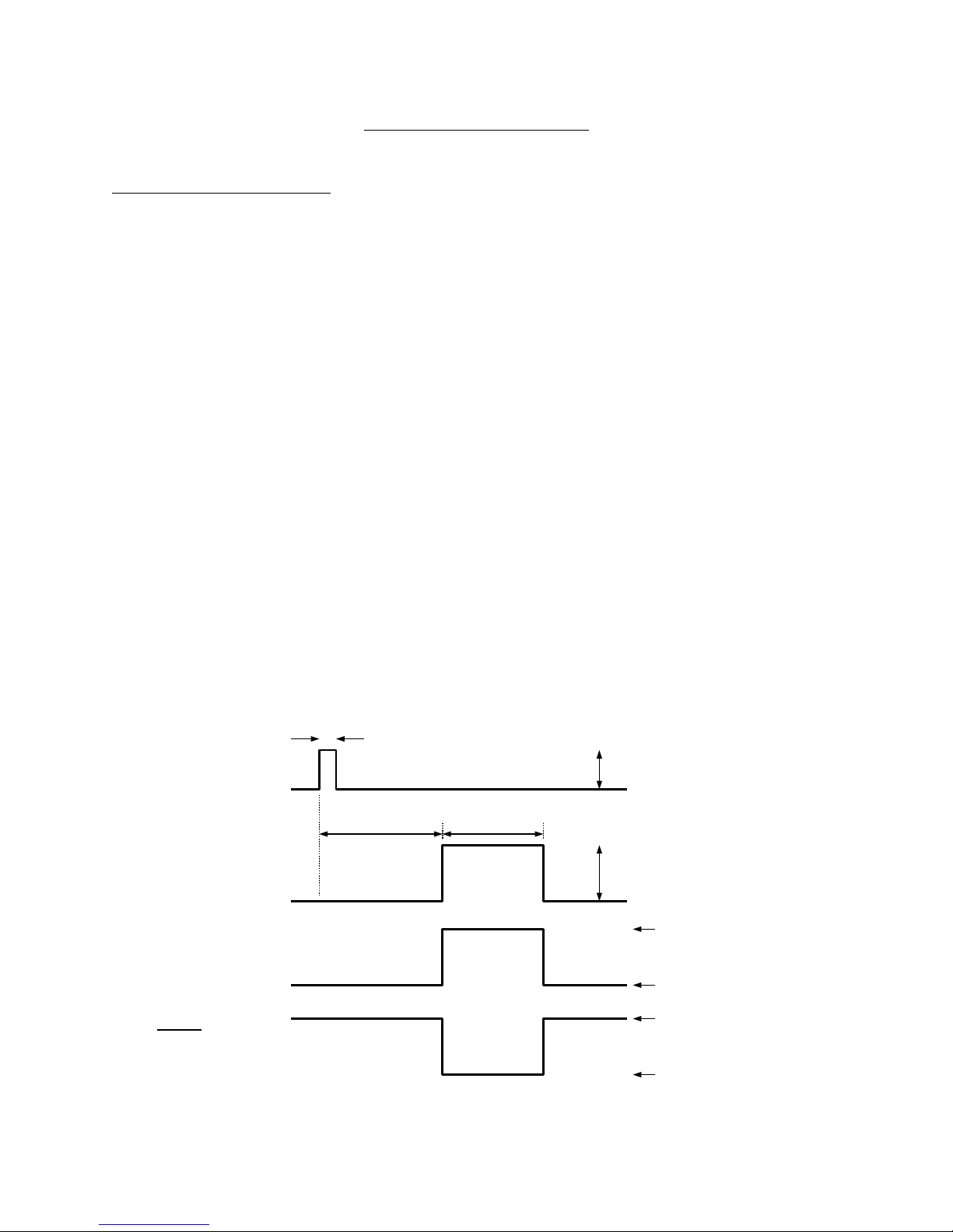
These pulses are illustrated below, assuming internal triggering and a positive delay:
SYNC OUT
(generated by the
internal oscillator)
MAIN OUTPUT
LOGIC OUTPUT
LOGIC OUTPUT
50 ns, FIXED
2V, FIXED
PULSE WIDTHDELAY > 0
AMPLITUDE, VARIABLE
+5V (TTL) or -0.8V (ECL)
0V (TTL) or -1.6V (ECL)
+5V (TTL) or -0.8V (ECL)
0V (TTL) or -1.6V (ECL)
Page 20

If the delay is negative, the order of the SYNC and OUT pulses is reversed:
20
SYNC OUT
(generated by the
50 ns, FIXED
3V, FIXED
internal oscillator)
DELAY < 0
PULSE WIDTH
AMPLITUDE, VARIABLE
MAIN OUTPUT
+5V (TTL) or -0.8V (ECL)
LOGIC OUTPUT
0V (TTL) or -1.6V (ECL)
+5V (TTL) or -0.8V (ECL)
LOGIC OUTPUT
0V (TTL) or -1.6V (ECL)
The next figure illustrates the relationship between the signals when an external TTLlevel trigger is used:
Page 21

> 4 ns
21
TRIG
(external input)
SYNC OUT
MAIN OUTPUT
LOGIC OUTPUT
LOGIC OUTPUT
TTL LEVELS
(0V and 3V-5V)
PROPAGATION DELAY (FIXED)
50 ns, FIXED
3V, FIXED
PULSE WIDTHDELAY > 0
AMPLITUDE, VARIABLE
+5V (TTL) or -0.8V (ECL)
0V (TTL) or -1.6V (ECL)
+5V (TTL) or -0.8V (ECL)
0V (TTL) or -1.6V (ECL)
As before, if the delay is negative, the order of the SYNC and OUT pulses is reversed.
The last figure illustrates the relationship between the signal when an external TTLlevel trigger is used in the PWIN=PW
mode. In this case, the output pulse width
OUT
equals the external trigger’s pulse width (approximately), and the delay circuit is
bypassed:
Page 22

PWI N
22
TRIG
(external input)
PROPAGATION DELAY (FIXED)
PWOUT ≈ PWIN
MAIN OUTPUT
LOGIC OUTPUT
LOGIC OUTPUT
TTL LEVELS
(0V and 3V-5V)
AMPLITUDE, VARIABLE
+5V (TTL) or -0.8V (ECL)
0V (TTL) or -1.6V (ECL)
+5V (TTL) or -0.8V (ECL)
0V (TTL) or -1.6V (ECL)
The delay, pulse width, and frequency (when in the internal mode), of the OUT pulse
can be varied with front panel controls or via the GPIB or RS-232 computer interfaces.
TRIGGER MODES
This instrument has four trigger modes:
• Internal Trigger: the instrument controls the trigger frequency, and generates the
clock internally.
• External Trigger: the instrument is triggered by an external TTL-level clock on the
back-panel TRIG connector.
• Manual Trigger: the instrument is triggered by the front-panel “SINGLE PULSE”
pushbutton.
• Hold Trigger: the instrument is set to not trigger at all.
These modes can be selected using the front panel trigger menu, or by using the
appropriate programming commands. (See the “Programming Manual for -B
Instruments” for more details.)
Page 23

PULSE WIDTH MODES
This instrument has two pulse width modes:
• Normal: the instrument controls the output pulse width.
23
• PW
=PW
IN
: the output pulse width equals the pulse width of the trigger signal on
OUT
the “TRIG” connector. The instrument must be in the external trigger mode.
These modes can be selected using the front panel pulse width menu, or by using the
appropriate programming commands. (See the “Programming Manual for -B
Instruments” for more details.)
PULSE WIDTH – AMPLITUDE INTERACTION
The pulse width may vary over a small range (± 5 ns) as the amplitude is varied. This is
normal, and unavoidable.
GATING MODES
Triggering can be suppressed by a TTL-level signal on the rear-panel GATE connector.
The instrument can be set to stop triggering when this input high or low, using the frontpanel gate menu or the appropriate programming commands. This input can also be
set to act synchronously or asynchronously. When set to asynchronous mode, the
GATE will disable the output immediately. Output pulses may be truncated. When set
to synchronous mode, the output will complete the full pulse width if the output is high,
and then stop triggering. No pulses are truncated in this mode.
Page 24

MINIMIZING WAVEFORM DISTORTIONS
USE 50 OHM TRANSMISSION LINES AND LOADS
Connect the load to the pulse generator with 50Ω transmission lines (e.g. RG-58 or
RG-174 cable).
This instrument requires a 50Ω load for proper operation. It will not properly drive a
high-impedance load.
USE LOW-INDUCTANCE LOADS
Lenz’s Law predicts that for an inductive voltage spike will be generated when the
current through an inductance changes. Specifically, V
the inductance, I
is the load current change, and t is time. For this reason, it is
LOAD
SPIKE
= L × dI
/dt, where L is
LOAD
important to keep any parasitic in the load low. This means keeping wiring short, and
using low inductance components. In particular, wire-wound resistors should be
avoided.
24
Page 25
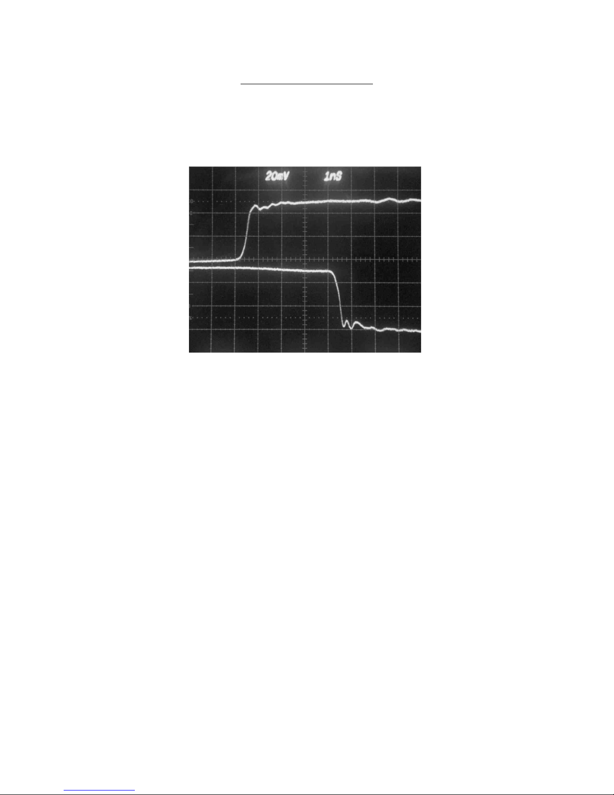
TYPICAL WAVEFORMS
The following waveform photo shows the rising and falling edges of the main output
with the AV-1030-B set to 100 kHz repetition rate, 100 ns pulse width, +5V amplitude,
into a 50 Ohm load:
25
Top: Rising edge
Bottom: Falling edge
Both: 2 V/div (i.e., 20 mV/div 40 dB), 1 ns/div
Page 26

26
OPERATIONAL CHECK
This section describes a sequence to confirm the basic operation of the instrument. It
should be performed after receiving the instrument. It is a useful learning exercise as
well.
Before proceeding with this procedure, finish reading this instruction manual
thoroughly. Then read the “Local Control” section of the “Programming Manual for -B
Instruments” thoroughly. The “Local Control” section describes the front panel controls
used in this operational check - in particular, the MOVE, CHANGE, and ADJUST
controls.
SAMPLING
OSCILLOSCOPE
BW > 5 GHz
50 OHM INPUT
TRIG
CONNECTOR
AC
POWER
AVTECH
PULSER
MAIN OUTPUT
CONNECTOR
40 dB
ATTENUATOR
TRIG
CONNECTOR
ALL CABLES: 50 OHM COAXIAL
BASIC TEST ARRANGEMENT
1.Connect the pulse generator to a sampling oscilloscope as shown above. Note that:
a)The use of 40 dB attenuator at the sampling scope vertical input channel will
insure a peak input signal to the sampling scope of less than 1 Volt. Factory tests
are conducted using Midwest Microwave model ATT-0444-20-SMA-02
attenuators.
b)The TRIG output channel provides TTL level signals (approximately 0 and +3V).
To avoid overdriving the TRIG input channel of some scopes, a 20 dB attenuator
may be required at the input of the scope trigger channel.
c)The bandwidth capability of components and instruments used to display the
pulse generator output signal (attenuators, cables, connectors, etc.) should
exceed 5 GHz.
Page 27

d)Set the oscilloscope to trigger externally with the vertical setting at 50 mV/div and
the horizontal setting at 10 ns/div.
2.Turn on the AV-1030-B. The main menu will appear on the LCD.
3.To set the AV-1030-B to trigger from the internal clock at a PRF of 10 kHz:
a)The arrow pointer should be pointing at the frequency menu item. If it is not, press
the MOVE button until it is.
b)Press the CHANGE button. The frequency submenu will appear. Rotate the
ADJUST knob until the frequency is set at 10 kHz.
c)The arrow pointer should be pointing at the “Internal” choice. If it is not, press
MOVE until it is.
d)Press CHANGE to return to the main menu.
4.To set the delay to 100 ns:
27
a)Press the MOVE button until the arrow pointer is pointing at the delay menu item.
b)Press the CHANGE button. The delay submenu will appear. Rotate the ADJUST
knob until the delay is set at 100 ns.
c)The arrow pointer should be pointing at the “Normal” choice. If it is not, press
MOVE until it is.
d)Press CHANGE to return to the main menu.
5.To set the pulse width to 50 ns:
a)Press the MOVE button until the arrow pointer is pointing at the pulse width menu
item.
b)Press the CHANGE button. The pulse width submenu will appear. Rotate the
ADJUST knob until the pulse width is set at 50 ns.
c)The arrow pointer should be pointing at the “Normal” choice. If it is not, press
MOVE until it is.
d)Press CHANGE to return to the main menu.
6.At this point, nothing should appear on the oscilloscope.
7.To enable the output:
Page 28

a)Press the MOVE button until the arrow pointer is pointing at the output menu item.
b)Press the CHANGE button. The output submenu will appear.
c)Press MOVE until the arrow pointer is pointing at the “ON” choice.
d)Press CHANGE to return to the main menu.
8.To change the output amplitude:
a)Press the MOVE button until the arrow pointer is pointing at the amplitude menu
item.
b)Press the CHANGE button. The amplitude submenu will appear. Rotate the
ADJUST knob until the amplitude is set at +5V.
c)Observe the oscilloscope. You should see 50 ns wide, 5V pulses. If you do not,
you may need to adjust the delay setting to a value more compatible with your
sampling oscilloscope. Repeat step 4 if required. You may also need to adjust the
sampling scope controls.
28
d)Rotate the ADJUST knob. The amplitude as seen on the oscilloscope should vary.
Return it to 5V.
e)Press the +/- button on the front panel. The amplitude as seen on the oscilloscope
should flip polarity, to -5V.
f) Press CHANGE to return to the main menu.
This completes the operational check.
Page 29

29
PROGRAMMING YOUR PULSE GENERATOR
KEY PROGRAMMING COMMANDS
The “Programming Manual for -B Instruments” describes in detail how to connect the
pulse generator to your computer, and the programming commands themselves. A
large number of commands are available; however, normally you will only need a few of
these. Here is a basic sample sequence of commands that might be sent to the
instrument after power-up:
*rst (resets the instrument)
trigger:source internal (selects internal triggering)
output:type TTL (sets the logic outputs to TTL mode)
frequency 1000 Hz (sets the frequency to 1000 Hz)
pulse:width 10 us (sets the pulse width to 10 us)
pulse:delay 1 us (sets the delay to 1 us)
volt:ampl 5 (sets the amplitude to 5 V)
output on (turns on the output)
For triggering a single event, this sequence would be more appropriate:
*rst (resets the instrument)
trigger:source hold (turns off all triggering)
output:type TTL (sets the logic outputs to TTL mode)
pulse:width 100 ns (sets the pulse width to 100 ns)
output on (turns on the output)
volt:ampl 5 (sets the amplitude to 5 V)
trigger:source immediate (generates a single non-repetitive trigger event)
trigger:source hold (turns off all triggering)
output off (turns off the output)
To set the instrument to trigger from an external TTL signal applied to the rear-panel
TRIg connector, use:
*rst (resets the instrument)
trigger:source external (selects internal triggering)
output:type TTL (sets the logic outputs to TTL mode)
pulse:width 10 us (sets the pulse width to 10 us)
pulse:delay 1 us (sets the delay to 1 us)
volt:ampl 5 (sets the amplitude to 5 V)
output on (turns on the output)
Page 30

In the above example, the pulse width of the output was set by a programming
command. To set the output pulse width to track the trigger pulse width in external
mode, use:
*rst (resets the instrument)
trigger:source external (selects internal triggering)
pulse:width in (PW
= PWIN)
OUT
output:type TTL (sets the logic outputs to TTL mode)
volt:ampl 5 (sets the amplitude to 5 V)
output on (turns on the output)
These commands will satisfy 90% of your programming needs.
ALL PROGRAMMING COMMANDS
For more advanced programmers, a complete list of the available commands is given
below. These commands are described in detail in the “Programming Manual for -B
Instruments”. (Note: this manual also includes some commands that are not
implemented in this instrument. They can be ignored.)
30
Keyword Parameter Notes
DIAGnostic:
:AMPLitude
:CALibration <numeric value> [no query form]
LOCAL
OUTPut:
:[STATe] <boolean value>
:PROTection
:TRIPped? [query only]
:TYPE TTL | ECL
REMOTE
[SOURce]:
:FREQuency
[:CW | FIXed] <numeric value>
[SOURce]:
:PULSe
:PERiod <numeric value>
:WIDTh <numeric value>
:DCYCle <numeric value>
:HOLD WIDTh | DCYCle
:DELay <numeric value>
:DOUBle
[:STATE] <boolean value>
:DELay <numeric value>
:GATE
:TYPE ASYNC | SYNC
:LEVel HIgh | LOw
[SOURce]:
:VOLTage
[:LEVel]
Page 31

[:IMMediate]
[:AMPLitude] <numeric value>
:PROTection
:TRIPped? [query only]
STATUS:
:OPERation
:[EVENt]? [query only, always returns "0"]
:CONDition? [query only, always returns "0"]
:ENABle <numeric value> [implemented but not useful]
:QUEStionable
:[EVENt]? [query only, always returns "0"]
:CONDition? [query only, always returns "0"]
:ENABle <numeric value> [implemented but not useful]
SYSTem:
:COMMunicate
:GPIB
:ADDRess <numeric value>
:SERial
:CONTrol
:RTS ON | IBFull | RFR
:[RECeive]
:BAUD 1200 | 2400 | 4800 | 9600
:BITS 7 | 8
:ECHO <boolean value>
:PARity
:[TYPE] EVEN | ODD | NONE
:SBITS 1 | 2
:ERRor
:[NEXT]? [query only]
:COUNT? [query only]
:VERSion? [query only]
TRIGger:
:SOURce INTernal | EXTernal | MANual | HOLD | IMMediate
*CLS [no query form]
*ESE <numeric value>
*ESR? [query only]
*IDN? [query only]
*OPC
*SAV 0 | 1 | 2 | 3 [no query form]
*RCL 0 | 1 | 2 | 3 [no query form]
*RST [no query form]
*SRE <numeric value>
*STB? [query only]
*TST? [query only]
*WAI [no query form]
31
Page 32

32
MECHANICAL INFORMATION
TOP COVER REMOVAL
If necessary, the interior of the instrument may be accessed by removing the four
Phillips screws on the top panel. With the four screws removed, the top cover may be
slid back (and off).
Always disconnect the power cord and allow the instrument to sit unpowered for 10
minutes before opening the instrument. This will allow any internal stored charge to
discharge.
There are no user-adjustable internal circuits. For repairs other than fuse replacement,
please contact Avtech (info@avtechpulse.com) to arrange for the instrument to be
returned to the factory for repair. Service is to be performed solely by qualified service
personnel.
Caution: High voltages are present inside the instrument during normal operation.
Do not operate the instrument with the cover removed.
RACK MOUNTING
A rack mounting kit is available. The -R5 rack mount kit may be installed after first
removing the one Phillips screw on the side panel adjacent to the front handle.
ELECTROMAGNETIC INTERFERENCE
To prevent electromagnetic interference with other equipment, all used outputs should
be connected to shielded loads using shielded coaxial cables. Unused outputs should
be terminated with shielded coaxial terminators or with shielded coaxial dust caps, to
prevent unintentional electromagnetic radiation. All cords and cables should be less
than 3m in length.
Page 33

MAINTENANCE
REGULAR MAINTENANCE
This instrument does not require any regular maintenance.
On occasion, one or more of the four rear-panel fuses may require replacement. All
fuses can be accessed from the rear panel. See the “FUSES” section for details.
CLEANING
If desired, the interior of the instrument may be cleaned using compressed air to
dislodge any accumulated dust. (See the “TOP COVER REMOVAL” section for
instructions on accessing the interior.) No other cleaning is recommended.
33
Page 34

WIRING DIAGRAMS
WIRING OF AC POWER
1 2 3 4 5 6
A
B
C
D
654321
D
C
B
A
T i t le
R e v i s i o nD a t e
3 - M a r - 2 0 1 1
Z : \m j c f i l e s \ p c b \1 5 8 \ s w i t c h i n g 6 0 h z .d d b - U S A G E \ Q C 3 v 5 E - A A D .s c h
Q C 3 H A R N E S S , F O R P C B 1 5 8 N , T A M U R A A A D
5 E
F A I L
3
N
L
V 1 S H R
2
V 2 S H R
1
R T N
4
V 1 - S N S
5
V 1 + S N S
6
V 2 + S N S
7
V 2 - S N S
8
V 1
4
V 1 R T N
3
V 2 R T N
2
V 2
1
G
P S 1
A A D 1 3 0 S D - 6 0 - A
O V
T E M P
A U X
A
K
YBR
O
Y
G
TO L C D
TO P C B 1 0 8
TO E N C O D E RTO L C D
1 0 4 D
B D 2
P C B 1 0 4 D K E Y P A D B O A R D ( - B U N I T S O N L Y )
+ 1 0 V
+ 1 5 V
+ 1 5 V
- 1 5 V
- 5 V
+ 5 V
+ 5 V
G N D
+ 2 4 V , N O O L O
+ 2 4 V , N O O L O
+ 1 0 V
+ 1 5 V
- 1 5 V
- 5 V
+ 5 V
G N D
G N D
+ 5 V
+ 5 V
+ 2 4 , N O O L O
G N D
P O S O L O
2 0 A W G
2 4 A W G
N E G O L O / + I N
G N D
O L O G N D
2 0 O R 2 4 A W G
C A P B A N K
G N D
E X T + P S I N
- I N / + O U T
G N D
G N D
G R E E N
G N D
A M B E R
S 1 A
S 1 B
D C / S 2 A
D C G N D
C H S G N D
S 2 B
2 0 A W G
P C B 1 5 8 N
+ 1 2 V O L O
G N D
K
A
-
+
J 1
J 2
J 3
J 4
J 5
J 6
J 7
J 8
+
J 9 - F A N
J 1 0
G N D
G N D
G N D
2 0 A W G
B D 1
P C B 1 5 8 N
C h a s s i s g r o u n d p o s t .
G 1
G 2
B 1 - R E D
G 4
G 3
L
N
G
X 2
C O R C O M 6 E G G 1 - 2 P O W E R E N T R Y M O D U L E
1
1 b
1 a
2
2 b
2 a
X 1
P O W E R S W I T C H S W 3 2 5 - N D (C W I N D U S T R I E S G R S - 4 0 2 2 - 0 0 1 3 )
A 1 - B R O W N
A 2 - B L U E
A 3 - B L A C K
A 4 - W H IT E
G R N
A M B
D 1
P 3 9 5 - N D L E D
G R N
A M B
B L K
R E D
W H T
X 5
V C C L E D M O U N T
D C
F A N
+
-
F A N 1
P 9 7 6 8 -N D
F A N N O T
C 3 - P U R
C 4 - G R N
M o le x 1 9 0 7 3 - 0 0 1 3 r i n g t e r m i n a l , # 8 .
M o le x 1 9 0 0 2 - 0 0 0 1 . 0 . 2 5 0 " x 0 . 0 3 2 " .
P r o t e c t i v e c o n d u c t o r t e r m in a l .
M o le x 1 9 0 0 2 - 0 0 0 9 . 0 . 1 8 7 " x 0 . 0 3 2 "
P r i m a r y e a r t h g r o u n d /
S a f e t y e a r t h g r o u n d /
S e c o n d a r y e a r t h g r o u n d .
In s t a l l g r e e n / y e l lo w w i r e s a t b o t t o m o f s t a c k , c lo s e s t t o w a ll .
M a in s c i r c u i t s - h a z a r d o u s l iv e .
W A R N I N G
D o n o t a tt e m p t a n y r e p a i r s o n th is in s t r u m e n t
b e y o n d t h e f u s e r e p la c e m e n t p r o c e d u r e s d e s c r i b e d
in th e m a n u a l . C o n ta c t A v t e c h if t h e i n s t r u m e n t
r e q u i r e s s e r v i c i n g . S e r v ic e i s t o b e p e r fo r m e d
s o l e ly b y q u a l if i e d s e r v i c e p e r s o n n e l .
H A R N E S S E D
U S E T IE - D O W N P O I N T O N P C B 1 5 8 N
F R O N T R E A R
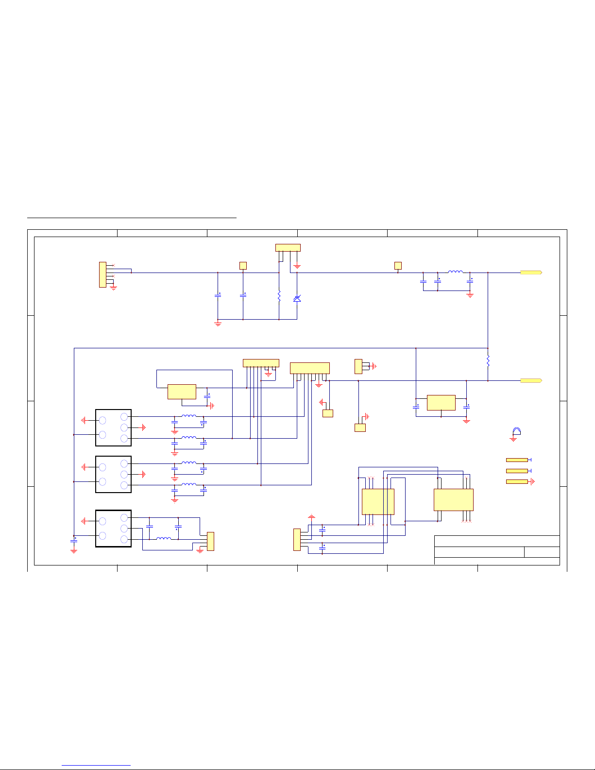
Page 35

PCB 158N - LOW VOLTAGE POWER SUPPLY, 1/3
1 2 3 4 5 6
A
B
C
D
654321
D
C
B
A
T i t l e
R e v i s i o nD a t e
1 2 - D e c - 2 0 0 8
Z : \ m j c f i l e s \ p c b \ 1 5 8 \ s w i t c h i n g 6 0 h z . d d b - 1 5 8 N \ p c b 1 5 8 N . s c h
L O W V O L T A G E D C / D C P O W E R S U P P L Y
123
J 5
6 4 0 4 5 6 - 3
1
2
3
4
5
6
7
8
J 4
6 4 0 4 4 5 - 8
1
2
3
4
5
6
J 3
6 4 0 4 4 5 - 6
+ 1 5 V
+ 1 5 V
B U +
P - O U T # 1
+ 1 5 V
G N D
- 1 5 V
p c b 1 5 8 N _ o v p
p c b 1 5 8 N _ o v p . s c h
B U +
P - O U T # 1
+ 1 5 V
G N D
- 1 5 V- 1 5 V
B U +
E X T
P - O U T # 2
N - O U T
N E G I N C A P B A N K
A M B E R
G R E E N
+ 1 5 V
G N D
- 1 5 V
P - O U T # 3P - O U T # 1
p c b 1 5 8 N _ s w i t c h i n g
p c b 1 5 8 N _ s w i t c h i n g . s c h
B U +
E X T
P - O U T # 2
N - O U T
N E G I N C A P B A N K
A M B E R
G R E E N
+ 1 5 V
G N D
- 1 5 V
P - O U T # 3P - O U T # 1
- 1 5 V
1
2
J 7
6 4 0 4 5 6 - 2
Page 36
PCB 158N - LOW VOLTAGE POWER SUPPLY, 2/3
1 2 3 4 5 6
A
B
C
D
654321
D
C
B
A
T i t l e
R e v i s i o nD a t e
1 2 - D e c - 2 0 0 8
Z : \ m j c f i l e s \ p c b \ 1 5 8 \ s w i t c h i n g 6 0 h z . d d b - 1 5 8 N \ p c b 1 5 8 N _ o v p . s c h
D C / D C , A N D O V E R - V O L T A G E P R O T E C T I O N
D 7
1 . 5 K E 3 9 A
T P 3
T E S T - L O O P
T P 6
T E S T - L O O P
A1A2B3X
4
F 3
8 3 0 8 3 5 F U S E H O L D E R
C 2 1
2 . 2 u F
C 2 0
4 7 u F , 5 0 V
L 5
4 3 4 - 1 3 - 1 0 0 M
B U +
C 1 9
4 7 u F , 5 0 V
1
2
3
4
5
6
J 6
6 4 0 4 4 5 - 6
S 1 A
S 1 B , O R D C
S 2 A , O R D C
S 2 B
V i n
1
G N D
2
V o u t
3
U 5
7 8 2 4 ( N O T N O R M A L L Y I N S T A L L E D )
C 1 3
4 7 u F , 5 0 V
C 7
4 7 u F , 5 0 V
R 5
0 , F O R 7 8 2 4 B Y P A S S . N O R M A L L Y I N S T A L L E D .
P - O U T # 1
V i n
1
G N D
2
V o u t
3
U 2
7 8 1 0
123456789
J 2
6 4 0 4 4 5 - 9
+ 1 0 V
- 1 5 V
- 5 V
+ 5 V
+
3
+
1
-
2
-
5
C
4
U 1
A S T R O D Y N E F E C 1 5 - 2 4 D 1 5 D C - D C
+
3
+
1
-
2
-
5
C
4
U 4
A S T R O D Y N E F E C 1 5 - 2 4 D 0 5 D C - D C
+ 1 5 V
C 1 1
2 . 2 u F
L 3
4 3 4 - 1 3 - 1 0 1 M
C 9
4 7 u F , 3 5 V
C 6
2 . 2 u F
L 2
4 3 4 - 1 3 - 1 0 1 M
C 3
4 7 u F , 3 5 V
C 1
4 7 u F , 3 5 V
C 8
2 . 2 u F
L 1
4 3 4 - 1 3 - 1 0 1 M
C 4
4 7 u F , 3 5 V
C 1 2
2 . 2 u F
L 4
4 3 4 - 1 3 - 1 0 1 M
C 5
4 7 u F , 3 5 V
123456789
1 0
J 1
1 - 6 4 0 4 5 6 - 0
+ 1 0 V
+ 1 5 V
+ 1 5 V
- 1 5 V
- 5 V
+ 5 V
+ 5 V
G N D
+ 2 4 V
+ 2 4 V
+ 1 5 V
G N D
+ 1 5 V
- 1 5 V - 1 5 V
1
2
J 8
2 2 - 0 4 - 1 0 2 1
C 2 2
1 0 0 0 u F , 3 5 V ( P 5 1 6 9 - N D )
C 1 6
1 0 0 0 u F , 3 5 V ( P 5 1 6 9 - N D )
1
2
J 9
6 4 0 4 4 5 - 2
1
2
3
J 1 0
6 4 0 4 5 6 - 3
R 2 0
1 0 K
X 6
T I E - D O W N - 3 5 0
- I N2- I N
3
N / C9N / C
1 0
N / C
1 1
+ O U T
1 4
N / C
1 5
- O U T
1 6
+ I N
2 2
+ I N
2 3
U 9
N O T U S E D ( S B 0 3 / S B 0 5 )
+ I N1- O U T
1 0
+ O U T
1 1
- I N
1 2
- I N
1 3
+ O U T
1 4
- O U T
1 5
+ I N
2 4
N / C
2
N / C
2 3
N / C
3
N / C
2 2
U 8
N O T U S E D ( M K C 0 3 )
1
2
3
4
5
J 1 1
N O T U S E D ( 6 4 0 4 4 5 - 5 )
C 2 7
N O T U S E D ( 4 7 u F , 5 0 V )
C 2 8
N O T U S E D ( 4 7 u F , 5 0 V )
I N +
I N -
O U T +
O U T -
G N D
+
3
+
1
-
2
-
5
C
4
U 1 0
N O T U S E D
C 3 1
N O T U S E D ( 2 . 2 u F C E R )
L 6
N O T U S E D ( 4 3 4 - 1 3 - 1 0 1 M )
C 3 0
N O T U S E D ( 4 7 u F , 3 5 V )
1
2
3
4
J 1 2
N O T U S E D ( 6 4 0 4 5 6 - 4 )
C 2 9
N O T U S E D ( 4 7 u F , 3 5 V )
N O R M A L L Y U N U S E D
Page 37

PCB 158N - LOW VOLTAGE POWER SUPPLY, 3/3
1 2 3 4 5 6
A
B
C
D
654321
D
C
B
A
T i t l e
R e v i s i o nD a t e
1 2 - D e c - 2 0 0 8
Z : \ m j c f i l e s \ p c b \ 1 5 8 \ s w i t c h i n g 6 0 h z . d d b - 1 5 8 N \ p c b 1 5 8 N _ s w i t c h i n g . s c h
O V E R - C U R R E N T P R O T E C T I O N
-
3
+2-
1
+
4
K 3
A Q Z 1 0 2
D 4
1 N 5 3 0 5
R 1 4
5 . 1 K
D 2
1 N 4 7 3 3 A
R 1 0
1 2 0 O Y
E X T
A1A2B3X
4
F 2
8 3 0 8 3 5 F U S E H O L D E R
-
3
+2-
1
+
4
K 1
A Q Z 1 0 2
-
3
+2-
1
+
4
K 2
O P T . A Q Z 1 0 2
D 1
1 N 4 7 3 6 A
V +
8
R E S E T
4
T R I G
2
T H R
6
C O N T
5
D I S
7
G N D
1
O U T
3
U 7
M C 1 4 5 5
R 7
7 5 K
R 1 1
4 . 7 K
R 9
3 K ( R O L O , A D J U S T )
+ 1 5 V
R 1 2
1 K
P - O U T # 2
81 0
Q 1 D
M P Q 2 2 2 2
13
Q 1 A
M P Q 2 2 2 2
N - O U TN E G I N
R 1
0 , I F - 1 5 V S W I T C H E D B Y O L O . N O T N O R M A L L Y I N S T A L L E D .
- 1 5 V
C A P B A N K
A M B E R
R 1 9
6 8 0
75
Q 1 B
M P Q 2 2 2 2
R 1 6
1 . 2 K
+ 1 5 V
R 1 8
1 . 2 K
G R E E N
C 1 0
4 7 u F , 5 0 V
T P 5
T E S T - L O O P
T P 4
T E S T - L O O P
1
2 3
4
K 4
P S 7 2 0 0 B - 1 A
+ 1 5 V
T P 2
T E S T - L O O P
T P 1
T E S T - L O O P
C 1 7
0 . 1 u F
C 1 4
4 7 u F , 3 5 V
C 1 5
0 . 1 u F
- 1 5 V
X 3
6 - 3 2 M O U N T
X 4
6 - 3 2 M O U N T
X 1 0
6 - 3 2 M O U N T
( A N Y 1 5 V , N O N - C M O S 5 5 5 )
1 41 2
Q 1 C
M P Q 2 2 2 2
D I S A B L E O L O W H E N C H A R G I N G .
S H O R T S O U T B A S E W H E N C H A R G I N G .
B U +
+ 1 5 V
G N D
- 1 5 V
X 1
K E Y S T O N E 6 2 1 B R A C K E T
R 1 5
0 , I F O L O U S E S I N T P S . N O R M A L L Y I N S T A L L E D .
R 1 7
0 , I F O L O U S E S E X T P S . N O T N O R M A L L Y I N S T A L L E D .
C 2 3
1 0 0 0 u F , 3 5 V ( P 5 1 6 9 - N D )
C 1 8
2 2 0 u F , 1 6 V ( P 5 1 3 9 - N D )
C 2
O P T . 1 0 0 0 u F , 3 5 V ( P 5 1 6 9 - N D )
R 2
O P T . 2 2 A Y
D 6
L 6 2 7 1 1
X 2
H V W A R N I N G
D 9
1 N 4 1 4 8
D 1 0
1 N 4 1 4 8
+ 1 5 V
D I S A B L E A T P O W E R - O F F
D I S A B L E A T P O W E R - O N
C 2 4
4 7 u F , 3 5 V
R 4
1 5 0
( + 1 5 V L A G S H V B Y 5 0 0 m s )
X 5
T R I M P O T A C C E S S
V i n
1
G N D
2
V o u t
3
U 3
7 8 1 2
C 2 5
4 7 u F , 5 0 V
R 2 1
1 . 5 K o r 1 . 8 K O Y
C 2 6
0 . 1 u F
P - O U T # 3
P - O U T # 1
R 3
3 0 0
R 2 2
3 0 0
R 8
W L A R 1 0 0 F E C T ( 0 . 1 O H M S )
4
3
2
15
K 5
O P T . G 2 R L - 1 4 - D C 2 4
1 2
3
D 5
2 5 C T Q 0 4 0 I N 2 9 4 - 1 0 5 1 - N D ( S 7 0 1 ) H E A T S I N K
R 6
4 7 0
R 1 3
4 7 0 , I F N O K 2 . N O R M A L L Y I N S T A L L E D .
-
3
+2-
1
+
4
K 6
O P T . A Q Z 1 0 2
R 2 4
4 7 0
R 2 3
4 7 0 , I F N O K 6 . N O R M A L L Y I N S T A L L E D .
R 2 5
W L A R 1 0 0 F E C T ( 0 . 1 O H M S )
- I N3G N D
2
+ I N
4
V +
5
O U T
1
U 6
L T 6 1 0 6 C S 5
R 2 6
1 5 K
R 2 7
1 0 0
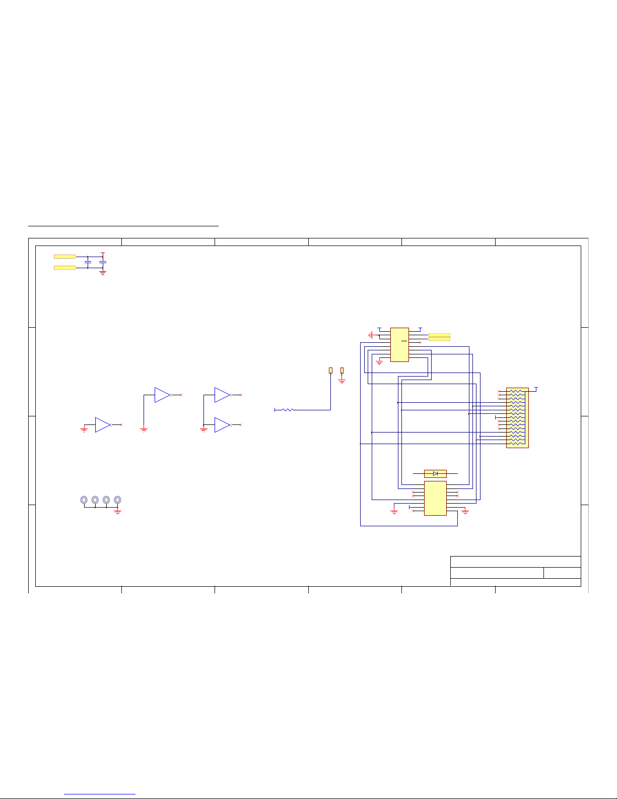
Page 38

PCB 104E - KEYPAD / DISPLAY BOARD, 1/3
1 2 3 4 5 6
A
B
C
D
654321
D
C
B
A
T i t l e
R e v i s i o nD a t e
3 - M a r - 2 0 1 1
Z : \m j c f i l e s \ p c b \ 1 0 4 e \ k e y p a d - 2 0 1 0 . d d b - D o c u m e n ts \ P a n e l b r d . p r j
P A N E L T O P - L E V E L S C H E M A T I C
1
2
3
4
5
6
7
8
9
1 0
J 5
A H E 1 0 G - N D , M f g 4 9 9 9 1 0 - 1 , 1 0 p i n s t r a i g h t h e a d e r
I 2 C _ I N T
S C L
S D A
G N D
V C C
S I N G L E P U L S E
B A C K L I G H T
E N C O D E R
E N C O D E R . S C H
I 2 C _ I N T
S C L
S D A
G N D
V C C
S I N G L E P U L S E
B A C K L I G H T
S D A
S C L
G N D
V C C
V C C - L E D
B A C K L I G H T
L C D - B U T T
L C D - B U T T . S C H
S D A
S C L
G N D
V C C
V C C - L E D
B A C K L I G H T
Page 39

PCB 104E - KEYPAD / DISPLAY BOARD, 2/3
1 2 3 4 5 6
A
B
C
D
654321
D
C
B
A
T i t l e
R e v i s i o nD a t e
3 - M a r - 2 0 1 1
Z : \m j c f i l e s \ p c b \ 1 0 4 e \ k e y p a d - 2 0 1 0 . d d b - D o c u m e n ts \ E N C O D E R . S C H
E N C O D E R , B U T T O N S , A N D P L D
V C C
A 0
1
A 1
2
A 2
3
P 0
4
P 1
5
P 2
6
P 3
7
G N D8P 4
9
P 5
1 0
P 6
1 1
P 7
1 2
I N T
1 3
S C L
1 4
S D A
1 5
V C C
1 6
U 3
P C F 8 5 7 4 A P N ( M U S T H A V E " A " I N P / N )
A 0
1
A 1
2
A 2
3
P 0
4
P 1
5
P 2
6
P 3
7
G N D8P 4
9
P 5
1 0
P 6
1 1
P 7
1 2
I N T
1 3
S C L
1 4
S D A
1 5
V C C
1 6
U 2
P C F 8 5 7 4 A P N ( M U S T H A V E " A " I N P / N )
I 2 C _ I N T
S C L
S D A
G N D
V C C
V C C
C 2
0 . 1 u F
C 4
0 . 1 u F
V C C
V C C
V C C
V C C
C 1 5
0 . 1 u F
C 1 3
0 . 1 u F
R E D , + 5 V
1
2
O R A N G E , B
3
Y E L L O W , A
4
G R E E N , G N D
5
X 6
6 0 0 E N -1 2 8 - C N 1
1 A 1 B
M O V E
2 A 2 B
X 1 0
3 A 3 B
+ / -
4 A 4 B
E X T R A F I N E
5 A 5 B
/ 1 0
6 A 6 B
C H A N G E
X 5
8 2 - 6 0 1 - 8 1 , 6 b u t t o n k e y p a d
A 0
1
A 1
2
A 2
3
P 0
4
P 1
5
P 2
6
P 3
7
G N D8P 4
9
P 5
1 0
P 6
1 1
P 7
1 2
I N T
1 3
S C L
1 4
S D A
1 5
V C C
1 6
U 7
P C F 8 5 7 4 A P N ( M U S T H A V E " A " I N P / N )
V C C
1 A 1 B
X 2
8 2 - 1 0 1 - 7 1 , 1 b u t t o n k e y p a d
12
U 4 A
M M 7 4 H C 1 4 N
1 11 0
U 1 E
M M 7 4 H C 1 4 N
S I N G L E P U L S E
V C C
V C C
C 1 0
2 . 2 u F
C 1 1
2 . 2 u F
C 1 2
2 . 2 u F
C 9
2 . 2 u F
C 7
2 . 2 u F
C 6
2 . 2 u F
C 1
2 . 2 u F
34
U 4 B
M M 7 4 H C 1 4 N
56
U 4 C
M M 7 4 H C 1 4 N
98
U 4 D
M M 7 4 H C 1 4 N
1 11 0
U 4 E
M M 7 4 H C 1 4 N
1 31 2
U 4 F
M M 7 4 H C 1 4 N
R 1
1 5 K
R 4
1 5 K
2345617
8
R N 3
4 6 0 8 X - 1 - 4 7 3
R 2
1 0 0 K
V C C
2
3
4
5
6
1
7
8
R N 2
4 6 0 8 X - 2 - 1 0 1
2
3
4
5
6
1
7
8
R N 1
4 6 0 8 X - 2 - 1 0 1
Q 1
M M B T 2 2 2 2 A
B U T 1
B U T 2
B U T 3
B U T 4
B U T 5
B U T 6
C N T 3
C N T 2
C N T 1
C N T 0
C N T 4
C N T 5
C N T 6
C N T 7
B U T 4
B U T 3
B U T 2
B U T 1
B U T 5
B U T 6
C 3
0 . 1 u F
V C C
1
2
J 8
6 4 0 4 5 6 - 2
1
2
3
J 7
6 4 0 4 5 6 - 3
A U X
O V
T E M P
C T E N
4
D / U
5
C L K
1 4
L O A D
1 1
M A X / M I N
1 2
R C O
1 3
A
1 5
Q A
3
B
1
Q B
2
C
1 0
Q C
6
D
9
Q D
7
U 6
C D 7 4 H C 1 9 1 M
C T E N
4
D / U
5
C L K
1 4
L O A D
1 1
M A X / M I N
1 2
R C O
1 3
A
1 5
Q A
3
B
1
Q B
2
C
1 0
Q C
6
D
9
Q D
7
U 8
C D 7 4 H C 1 9 1 M
9 8
U 1 D
M M 7 4 H C 1 4 N
C N T 4
C N T 5
C N T 6
C N T 7
C N T 0
C N T 1
C N T 2
C N T 3
V C C
C 1 4
0 . 1 u F
V C C
C 1 6
0 . 1 u F
Page 40
PCB 104E - KEYPAD / DISPLAY BOARD, 3/3
1 2 3 4 5 6
A
B
C
D
654321
D
C
B
A
T i t l e
R e v i s i o nD a t e
3 - M a r - 2 0 1 1
Z : \m j c f i l e s \ p c b \ 1 0 4 e \ k e y p a d - 2 0 1 0 . d d b - D o c u m e n ts \ L C D - B U T T . S C H
L C D C I R C U I T S , M E C H A N I C A L
A 0
1
A 1
2
A 2
3
P 0
4
P 1
5
P 2
6
P 3
7
G N D8P 4
9
P 5
1 0
P 6
1 1
P 7
1 2
I N T
1 3
S C L
1 4
S D A
1 5
V C C
1 6
U 5
P C F 8 5 7 4 A P N ( M U S T H A V E " A " I N P / N )
V C C
S D A
S C L
V C C
V C C
G N D
V C C
V C C
C 5
0 . 1 u F
D B 71D B 6
2
D B 53D B 4
4
D B 35D B 2
6
D B 17D B 0
8
E 19R / W
1 0
R S
1 1
V E E
1 2
V S S
1 3
V C C
1 4
E 2
1 5
N C
1 6
A K
X 1 0
AHE16G-ND, Mfg 499910-3, 16 pin straight header
1 2
U 1 A
M M 7 4 H C 1 4 N
1 3 1 2
U 1 F
M M 7 4 H C 1 4 N
5 6
U 1 C
M M 7 4 H C 1 4 N
P A D 3
L E D +
P A D 4
L E D -
X 3
4 - 4 0 M O U N T
X 1
4 - 4 0 M O U N T
X 9
4 - 4 0 M O U N T
X 8
4 - 4 0 M O U N T
3 4
U 1 B
M M 7 4 H C 1 4 N
L C D P O W E R
V C C
2
3
4
5
6
1
7
8
1 6
9
1 0
1 1
1 2
1 3
1 4
1 5
R N 4
4 8 1 6 P - 0 0 2 - 1 0 2
V C C
V C C
C 8
2 . 2 u F
R 3
2 2
Page 41
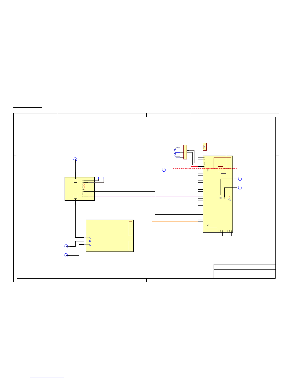
MAIN WIRING
1 2 3 4 5 6
A
B
C
D
654321
D
C
B
A
R e v i s i o nP r i n t e d
1 2 - A p r - 2 0 0 7
Z : \ m j c f i l e s \ c i r c u i t s \ A V - 1 0 3 0 \ 1 0 3 0 . d d b - A V - 1 0 3 0 - B \ 1 0 3 0 - B V 3 . S C H
A V - 1 0 3 0 - B W I R I N G
3 A
P O L - A
A M P
R 1 - B
R 2 - C
I N
- 1 5 V
+ 1 5 V
O U T ( R E A R )
M 1
A V - 1 0 3 0 - P G , M T A
M A I N O U T P U T
9 - P I N P O W E R H A R N E S S
2 6 - L I N E R I B B O N
< < I N D E X W I R E
O R A N G E
B L U E
N O T L O G I C
L O G I C
B D 1
A V - 1 0 2 1 - B B O A R D
C O N N 4
G A T E
C O N N 5
E X T T R I G
C O N N 3
S Y N C
A M P L I T U D E , 0 - 1 0 V
1
O F F S E T , 0 - 1 0 V
2
P W , 0 - 1 0 V
3
S P A R E , 0 - 1 0 V
4
O . P O L
5
O . Z O U T
6
O . L O G I C
7
O . S Q U
8
O . T R I
9
O . S I N E
1 0
O . E A
1 1
O . L E D
1 2
A M P L R N G 4
1 3
A M P L R N G 3
1 4
A M P L R N G 2
1 5
A M P L R N G 1
1 6
A M P L R N G 0
1 7
X R L Y 5
1 8
X R L Y 4 ( E O )
1 9
X R L Y 3 ( V - I )
2 0
X R L Y 2 ( D U A L P W )
2 1
X R L Y 1
2 2
G A T E
2 3
E X T T R I G
2 4
S Y N C O U T
2 5
M A I N O U T
2 6
+ 5 V O N / O F F
2 7
+ 1 5 V O N / O F F
2 8
T R I G O U T
S Y N C
L N K
R E D
G N D
B L K
N OCN C
E A I N
I N T
R N G
E X T
A C T
W H T
V S P A R E
V P R F
G A T E
T R I G
E A
B D 2
O P 1 B M A I N B O A R D , P C B 1 0 8 R
G R N
A M B
D 1
P 3 9 5 - N D L E D
X 1
V C C L E D M O U N T
C O N N 2
L - C O M E C F 5 0 4 - S C 5
- T N T O P T I O N O N L Y
L - C O M T R D 8 5 5 S I G - 1 C A B L E
- 1 5 V + 1 5 V
C O N N 7
L O G I C
C O N N 6
N O T - L O G I C
C O N N 1
O U T
Page 42

PERFORMANCE CHECK SHEET
42
 Loading...