

Page 1
Copyright © 2018 Avnet, Inc. AVNET, “Reach Further” and Avnet logo are registered
trademarks of Avnet, Inc. All other brands are the property of their respective owners.
LIT#
Global LTE IoT Starter Kit
Hardware User Guide
Version 1.4
Page 2

Page 2
Version
Date
Comment
1.0
07/05/2017
Initial Release
1.1
11/02/2017
Certification info added (pg 47-48)
1.2
12/04/2017
Section 4.5 cellular operating frequency bands amended
1.3
12/05/2017
Cellular operating frequency bands updated
1.4
02/10/2017
- Kit Contents diagram added
- Block Diagram updated
- URL for kit purchase updated
- Light Sensor cautionary note added
- Force USB Boot details added
- Additional GPIOs and notes on usage added
- Detailed info added to certification section
- Modem-mode use case removed
- Starter SIM details and supported countries updated
- Intro to LTE IoT Breakout Carrier plus use of Click modules for prototyping
Document Control
Document Version: 1.4
Document Date: 02/10/2018
Document Author: Peter Fenn
Document Classification: Public
Document Distribution: Public
Prior Version History
Page 3

Page 3
Contents
Terminology ..................................................................................................................... 7
1 Introduction ............................................................................................................... 8
1.1 Kit Info ................................................................................................................................. 9
1.2 Items Included in the Kit....................................................................................................... 9
2 Block Diagram and Features .................................................................................. 10
2.1 List of Features .................................................................................................................. 10
2.1.1 LTE System Board ..................................................................................................... 10
2.1.2 WNC M18QWG Global Module .................................................................................. 10
2.1.3 Pulse Electronics LTE + GNSS Antennas ................................................................... 10
2.1.4 Expansion Interfaces for System-Level Prototyping .................................................... 10
2.2 LTE IoT System Board Block Diagram ............................................................................... 12
2.3 Location of Key Components ................................................................ ............................. 13
3 LTE System Board Functional Description ............................................................ 14
3.1 LTE Modem Module (WNC M18QWG) .............................................................................. 14
3.2 Expansion Connector ........................................................................................................ 16
3.3 2x6 Pin Peripheral Connector ............................................................................................ 21
3.4 WNC Module Interfaces ..................................................................................................... 22
3.4.1 SIM Interface (3FF Micro-SIM Connector) .................................................................. 22
3.4.2 USB Interface ............................................................................................................ 23
3.4.3 UART1 Interface ........................................................................................................ 25
3.4.4 UART2 – Software Debug UART Interface (3-pin header) .......................................... 25
3.4.5 Voltage Level Translation (1.8V / 3.3V) ...................................................................... 26
3.4.6 ADC / Ambient Light Sensor (JP2) ............................................................................. 27
3.4.7 3D Accelerometer Sensor (LIS2DW12) ...................................................................... 28
3.4.8 Pushbutton Switches (Reset, User, Boot) ................................................................... 29
3.4.9 LED Status Indicators (Power, WWAN, User) ............................................................. 30
3.4.10 PCM / I2S Digital Audio Interface ............................................................................... 31
3.4.11 Ethernet SGMII Interface ............................................................................................ 32
3.4.12 User GPIO ................................................................................................................. 33
3.5 Power Regulation .............................................................................................................. 34
3.5.1 VIN ............................................................................................................................ 34
3.5.2 3V8 (VCC) ................................................................ ................................................. 34
3.5.3 1V8_VREF (VREF) .................................................................................................... 36
3.5.4 VCC_UIM_SIM (UIM_VCC) ....................................................................................... 36
3.5.5 3V3 ............................................................................................................................ 36
3.7 WNC Module Power Control and State Interfaces .............................................................. 37
Page 4

Page 4
3.8 Antennas ........................................................................................................................... 39
3.8.1 LTE Antennas (Primary, Diversity).............................................................................. 39
3.8.2 GPS Antenna ............................................................................................................. 40
4 Specifications and Ratings ..................................................................................... 42
4.1 Absolute Maximum Ratings ............................................................................................... 42
4.2 Recommended Electrical Operating Conditions ................................................................. 42
4.3 Power Consumption .......................................................................................................... 42
4.4 RF Characteristics ............................................................................................................. 43
4.5 Networking and Carrier ...................................................................................................... 43
4.6 GNSS Receiver Performance ............................................................................................ 44
4.7 Environmental ................................................................................................................... 44
4.8 Mechanical ................................................................ ........................................................ 45
5 Certifications ........................................................................................................... 47
5.1 RoHS Compliance ............................................................................................................. 47
5.2 Regulatory and Network Certifications ............................................................................... 47
5.2.1 Certification Documents ................................ ................................ ............................. 47
5.2.2 CE-RED: EMC Testing ............................................................................................... 47
5.2.3 CE-RED: Radio Testing ............................................................................................. 47
5.2.4 Electrical Safety Certification ...................................................................................... 47
6 Shipping, Handling and Storage ............................................................................ 48
6.1 Shipping ............................................................................................................................ 48
6.2 Handling ............................................................................................................................ 48
6.3 Storage ............................................................................................................................. 48
7 Safety Recommendations ...................................................................................... 48
8 Ordering Information ............................................................................................... 49
8.1 LTE System Board Accessories ......................................................................................... 49
8.1.1 Expansion Connector Options for Custom User Board ............................................... 49
8.1.2 Pulse FPC Antenna Options ....................................................................................... 49
9 Contact Information ................................................................................................ 51
10 Technical Support ................................................................................................... 51
11 Disclaimer ............................................................................................................... 51
12 Appendix A – LTE IoT Breakout Carrier ................................................................ 52
Page 5

Page 5
Figures
Figure 1 – Global LTE IoT Starter Kit Contents ............................................................. 9
Figure 2 – LTE IoT System Board – Block Diagram .................................................... 12
Figure 3 – LTE IoT System Board – Feature Identification ......................................... 13
Figure 4 – Global LTE Cat.4 IoT System Board........................................................... 13
Figure 5 – Internal view of the similar WNC M18Q2 series module ............................ 14
Figure 6 – Use Cases for Avnet LTE IoT Boards ......................................................... 15
Figure 7 – 3D View of Samtec ERF8 / ERM8 Connector Pair..................................... 16
Figure 8 – Expansion Connector Polarization .............................................................. 17
Figure 9 – Expansion Connector Board Stack Profile-View ........................................ 17
Figure 10 – Expansion Connector Pin Numbering ....................................................... 20
Figure 11 – 2x6 Peripheral Connector Board Edge-View ............................................ 21
Figure 12 – USB Interface Drivers Enumerate on Windows Host Computer ............. 24
Figure 13 – Board Detail Showing Light Sensor (U3) .................................................. 27
Figure 14 – CODEC Interface Using PCM or I2S ........................................................ 31
Figure 15 – Sleep and Power Control of WNC Module ............................................... 38
Figure 16 – Detail of U.FL Antenna Connectors .......................................................... 39
Figure 17 – GPS Antenna Circuit Diagram .................................................................. 40
Figure 18 – Mechanical Details (1 of 2) ........................................................................ 45
Figure 19 – Pulse FPC Antenna Options ..................................................................... 50
Figure 20 – LTE IoT Breakout Carrier (plus Click Modules) ........................................ 52
Page 6

Page 6
Tables
Table 1 – Summary of Key Specifications for LTE System Board .............................. 11
Table 2 – J1 Expansion Connector Pinout (Inner Row) ............................................... 18
Table 3 – J1 Expansion Connector Pinout (Outer Row) .............................................. 19
Table 4 – 2x6 Pmod Peripheral Connector Pinout ....................................................... 21
Table 5 – SIM Card Interface Connections .................................................................. 22
Table 6 – WNC USB Interface Connections ................................................................ 23
Table 7 – USB Logical Interfaces Reported by Windows Device Manager ................ 24
Table 8 – Software Debug UART Header (J9) ............................................................. 25
Table 9 – ADC Input Source Selector (JP2)................................................................. 27
Table 10 – LIS2DW12 Interrupt Outputs ...................................................................... 28
Table 11 – Pushbutton Switch Functions ..................................................................... 29
Table 12 – LED Indicator Functions ............................................................................. 30
Table 13 – PCM / I2S Digital Audio Interface Pins ...................................................... 31
Table 14 – GPIO Signals Available on Expansion Connector ..................................... 33
Table 15 – GPIO Signals Assigned Local Functions ................................................... 33
Table 16 – Summary of LTE System Board Voltages ................................................. 34
Table 17 – Control and State Signals ........................................................................... 37
Table 18 – WAKEUP_IN and WAKEUP_OUT ............................................................. 37
Table 19 – FPC Antenna Options from Pulse .............................................................. 39
Table 20 – Absolute Maximum Ratings ........................................................................ 42
Table 21 – Recommended Electrical Operating Conditions ........................................ 42
Table 22 – Power Consumption ................................................................................... 42
Table 23 – TX Power and RX Sensitivity ..................................................................... 43
Table 24 – Networking and Carrier Characteristics (Europe Operation) .................... 43
Table 25 – GNSS receiver performance ...................................................................... 44
Table 26 – Environmental Characteristics .................................................................... 44
Table 27 – Mechanical Characteristics......................................................................... 45
Table 28 – Certified Pulse Antennas ............................................................................ 47
Table 29 – Ordering Information ................................................................................... 49
Table 30 – Height options for Samtec ERM8 Expansion Connector .......................... 49
Table 31 – FPC Antenna Options from Pulse .............................................................. 49
Table 32 – Contact Information .................................................................................... 51
Page 7

Page 7
Terminology
Abbreviation
Definition
AC
Alternating Current
CE
European Conformity (Conformité Européene)
DC
Direct Current
ETSI
European Telecommunications Standards Institute
FCC
Federal Communications Commission
GND
Ground
GPIO
General Purpose Input / Output
I/O
Input / Output
IoT
Internet of Things
I2C
Inter-Integrated Circuit
JTAG
Joint Test Action Group
MEMs
Micro-Electro-Mechanical Systems
LTE
Long Term Evolution
N/A
Not Applicable
N/C
Not Connected
PIN
Personal Identification Number
Pmod
Peripheral module (Digilent Inc. trademark)
SIM
Subscriber Identity Module
SoC
System on Chip
SoM
System on Module
SPI
Serial Peripheral Interface
UART
Universal Asynchronous Receiver/Transmitter
UIM
User Identity Module
USB
Universal Serial Bus
Vref
Voltage reference
WCDMA
Wideband Code Division Multiple Access
WNC
Wistron NeWeb Corporation
Page 8

Page 8
1 Introduction
The Global LTE IoT Starter Kit is a next-generation System-on-Module IoT solution, enabling the design
of cellular connected edge devices, for operation in Europe.
Powered by AT&T IoT services available through Avnet, this kit provides a complete development
environment for sensor-to-cloud applications and services.
Designed to be used for both prototyping and production, the slim form-factor LTE System Board with it’s
regional certifications and pre-registered Micro-SIM card for AT&T M2X service (included in the kit), as
well as versatile expansion options, together provide a high level of enablement that facilitates easy IoT
deployment and reduction in overall risk.
The Starter Kit features a small (79.5 mm x 30 mm) LTE System Board built around a Wistron NeWeb
(WNC) M18QWG global LTE Cat-4 modem module. The M18QWG module provides cellular modem
functionality plus an applications processor core dedicated for user applications, eliminating the need for
an external host processor. A rich set of embedded system peripherals, controllable through the user’s
application code, are easily accessible via a 60-pin expansion connector and 2x6 peripheral module
header. This enables easy system customization with application specific sensors and I/O interfaces
through the addition of user-created or off-the-shelf plug-in boards. The LTE System Board includes
ambient light, temperature and accelerometer sensors onboard, for out-of-box demonstration examples.
User application code runs directly on the M18QWG module, leveraging the OpenEmbedded software
framework for Linux application development. A Software Development Kit (SDK) specific to the
M18QWG module provides the necessary API calls to access hardware peripherals and system
resources. Application code built with the SDK is loaded into the M18QWG module through a USB
interface on the development board eliminating the need for external proprietary JTAG cables.
Cloud application development is supported by AT&T’s M2X Data Services and Flow Designer.
- M2X is a cloud-based, fully managed data storage service for connected machine-to-machine
(M2M) devices
- Flow Designer provides a visual editing environment for the design of connected applications,
enabling IoT developers to rapidly create and deploy innovative new applications.
Design goals of this LTE IoT Starter Kit included the following:
- Provide a versatile prototyping- and production-ready (cost-optimized) platform for development
and productized custom applications using WNC M18QWG Cat.4 cellular modem and GPS, for
deployment Globally via AT&T’s partner LTE networks
- Provide hardware expansion examples using:
- PmodTM-compatible peripheral boards,
- Custom breakout board
- Provide reference designs that accelerate development of applications for popular use cases
- With the provided AT&T SIM starter pack, demonstrate the use of:
- AT&T M2X and Flow Designer
- Additional 3rd party cloud services such as AWS, Watson IoT, and Azure
Page 9
Page 9
1.1 Kit Info
Part Number: AES-ATT-M18QWG-SK-G
Price: $139.00 USD
Kit URL: http://cloudconnectkits.org/product/global-lte-starter-kit
Buy Page: AES-ATT-M18Q2FG-SK-G
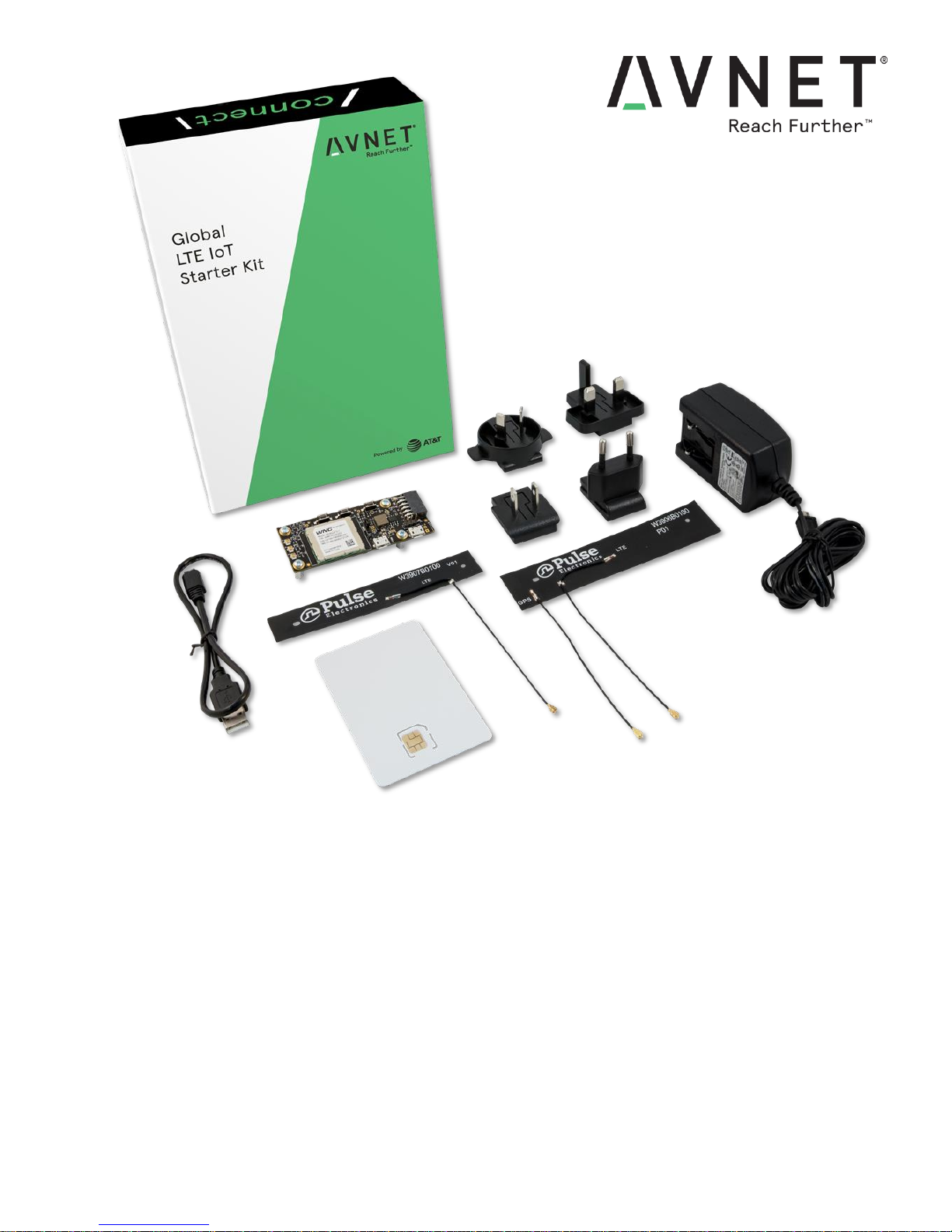
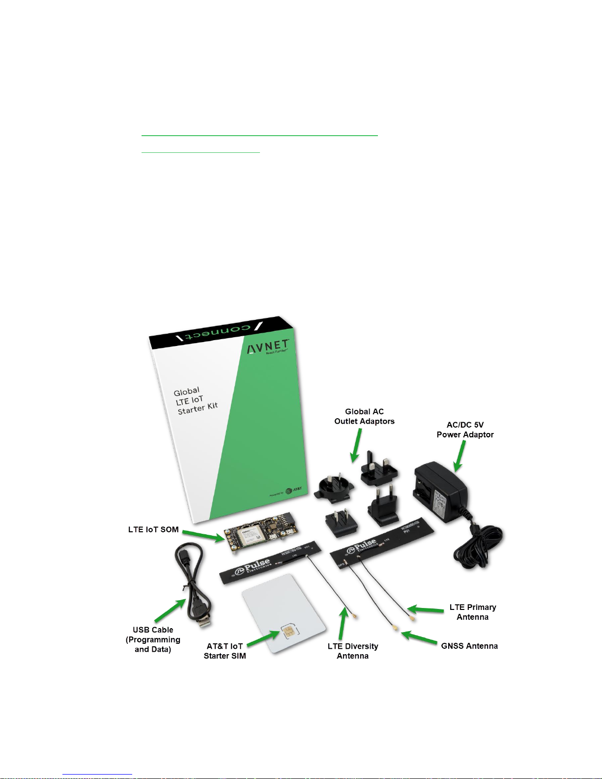
1.2 Items Included in the Kit
• LTE System Board (p/n: AES-ATT-M18QWG-M1-G )
• Pulse FPC antennas (LTE Primary Antenna, GPS Antenna, LTE Diversity Antenna)
• Micro-SIM card (100K data points on AT&T M2X IoT platform services plus 200 SMS messages,
good for 60 days from activation)
• Universal AC/DC power supply with regional adaptors (5V @ 2.5A)
• USB Cable for programming and debug)
Figure 1 – Global LTE IoT Starter Kit Contents
Page 10

Page 10
2 Block Diagram and Features
This section summarizes the features of the development board, followed by functional descriptions.
2.1 List of Features
The following features are supported:
2.1.1 LTE System Board
M18QWG Global LTE SoC Module
Ambient Light Sensor
3-Axis Accelerometer
Temperature Sensor
USB Interface
60-pin High-density Expansion Connector (1.8V levels)
2x6 Peripheral Module Connector (3.3V levels)
Power Regulation
2.1.2 WNC M18QWG Global Module
Supports Global LTE bands 1/2/3/5/7/8/20/28/38/40
Cat-4 LTE (up to 150/50 Mbps Download/Upload)
2G/3G Fallback
GPS
Based on Qualcomm MDM9207
o ARM® Cortex™ A7 Quad Core
o One of the A7 cores is dedicated for User Application
Rich Peripheral Features
2.1.3 Pulse Electronics LTE + GNSS Antennas
Three antennas implemented as two foldable FPC antenna-assemblies
2G/3G/4G MIMO
GNSS (GPS, Glonass)
Antenna interface to the LTE System board is via three space-efficient U.FL connectors
2.1.4 Expansion Interfaces for System-Level Prototyping
Two interfaces facilitate the adding of custom hardware to the LTE System board:
System expansion interface (1.8V I/O) is a 60 pin expansion connector (Samtec ERF8 /
ERM8 series) on the underside of the system board. WNC module peripherals are accessible
via this interface at 1.8V signalling levels, if 3.3V (or 2.5V) levels are required by the user’s
custom circuitry, then voltage translator devices must be added to the user’s board.
Pmod™-compatible interface (3.3V I/O) is 6x2 pin connector facilitates an easy to use
interface via I2C or SPI peripherals, for access to a wide range of Pmod™ peripheral boards.
The relaxed pitch of this connector and low pin count of these interfaces also permits wiring-in
other 3.3V expansion boards (eg. MikroElektronika Click modules or Grove sensor boards) for
prototyping system-level solutions
Page 11

Page 11
Table 1 – Summary of Key Specifications for LTE System Board
Product Parameter
Relevant Characteristics
MSRP
$99 @ 100+ units
Description
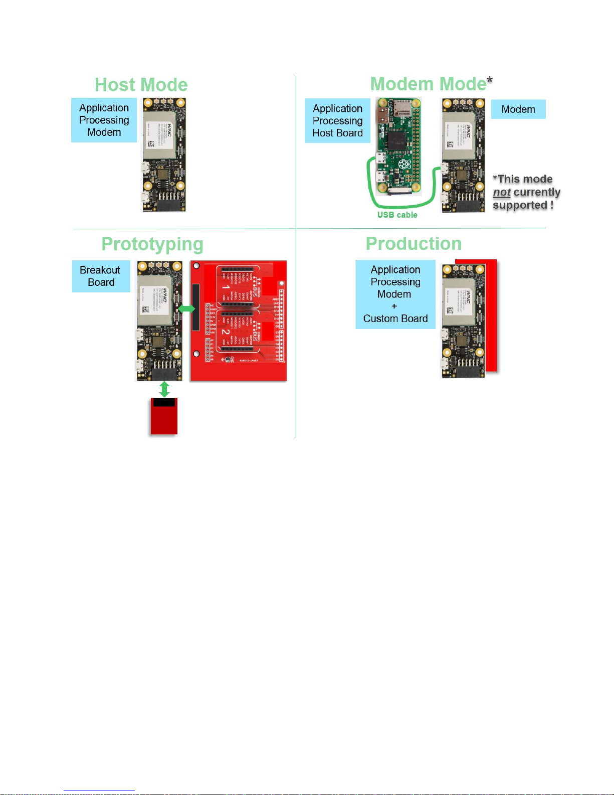
Embedded LTE and GPS system board offering two modes of operation:
- Host mode
- Modem mode (aka Slave mode. No Avnet support for this mode currently)
Application Interface
WNC API (Host mode only)
WNC AT Commands
Cellular Technology
LTE Cat.4, bands 1/3/7/8/20/28/38/40 (up to 150/50 Mbps DL/UL)
WCDMA, bands 1/8, 3GPP release 8
GSM, E-GSM 900, DCS 1800
GNSS Location Tracking
GPS, GLONASS (-162 dBm tracking sensitivity)
Peripheral Interfaces
HS USB 2.0 w/ PHY, SGMII, HSIC, UARTs (4 wire and 2 wire),
SDC1/SPI1, I2C/SPI2, USIM, GPIOs, ADC, PCM/I2S, JTAG
Power Consumption
See datasheet (utilizes power-efficient ARM Cortex-A7 technology)
Supply Voltage
4.5 V to 16 V DC
Expansion Interfaces
Pmod™-compatible connector (3.3V levels, 2x6 pin, 2.54 mm pitch)
SAMTEC ERM8 60pin connector (1.8V levels, 2x30pin, 0.8 mm pitch)
End-Device Certified
Regulatory and network certifications planned for Europe only
Data Service
Starter SIM includes:
- 100K data points on AT&T M2X service,
- 200 SMS messages,
- good for 60 days from activation
Data Interface
N/A in Host mode
Dimensions (mm)
79.5mm x 30 mm
Warranty
1 year
Page 12
Page 12
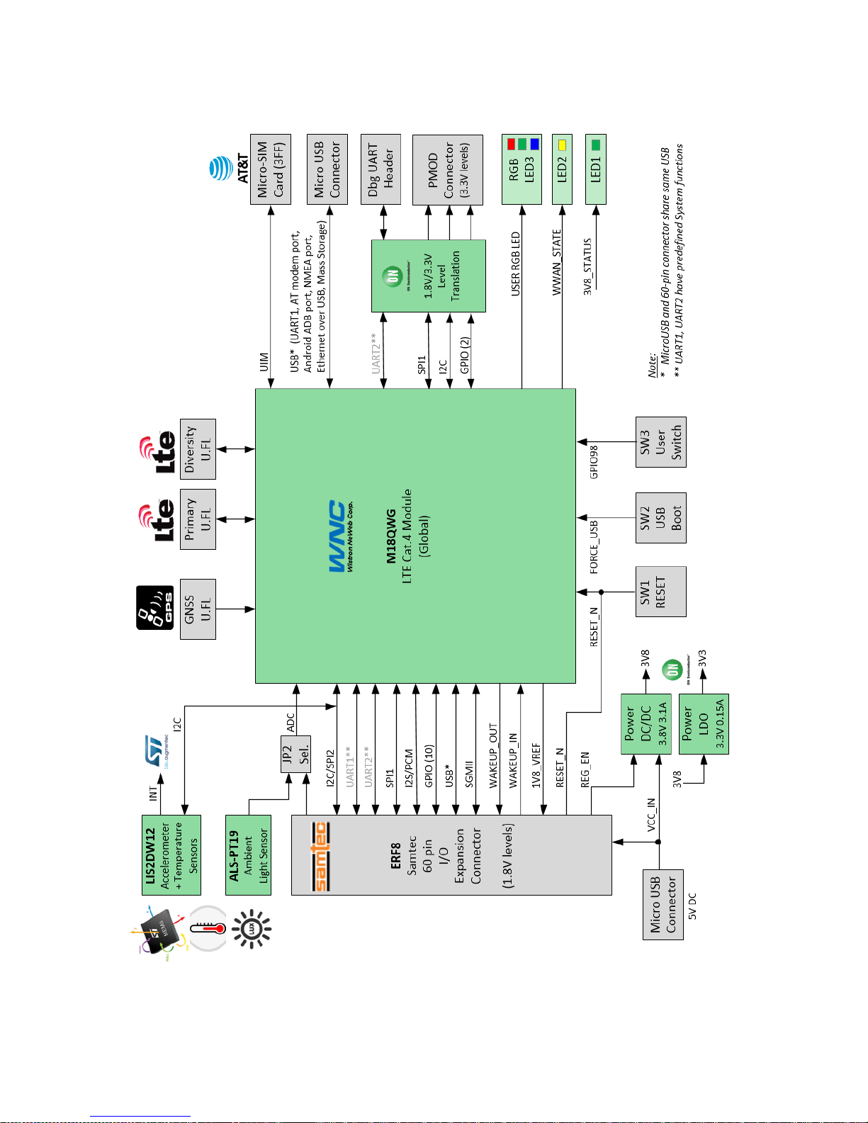
2.2 LTE IoT System Board Block Diagram
Figure 2 – LTE IoT System Board – Block Diagram
Page 13
Page 13
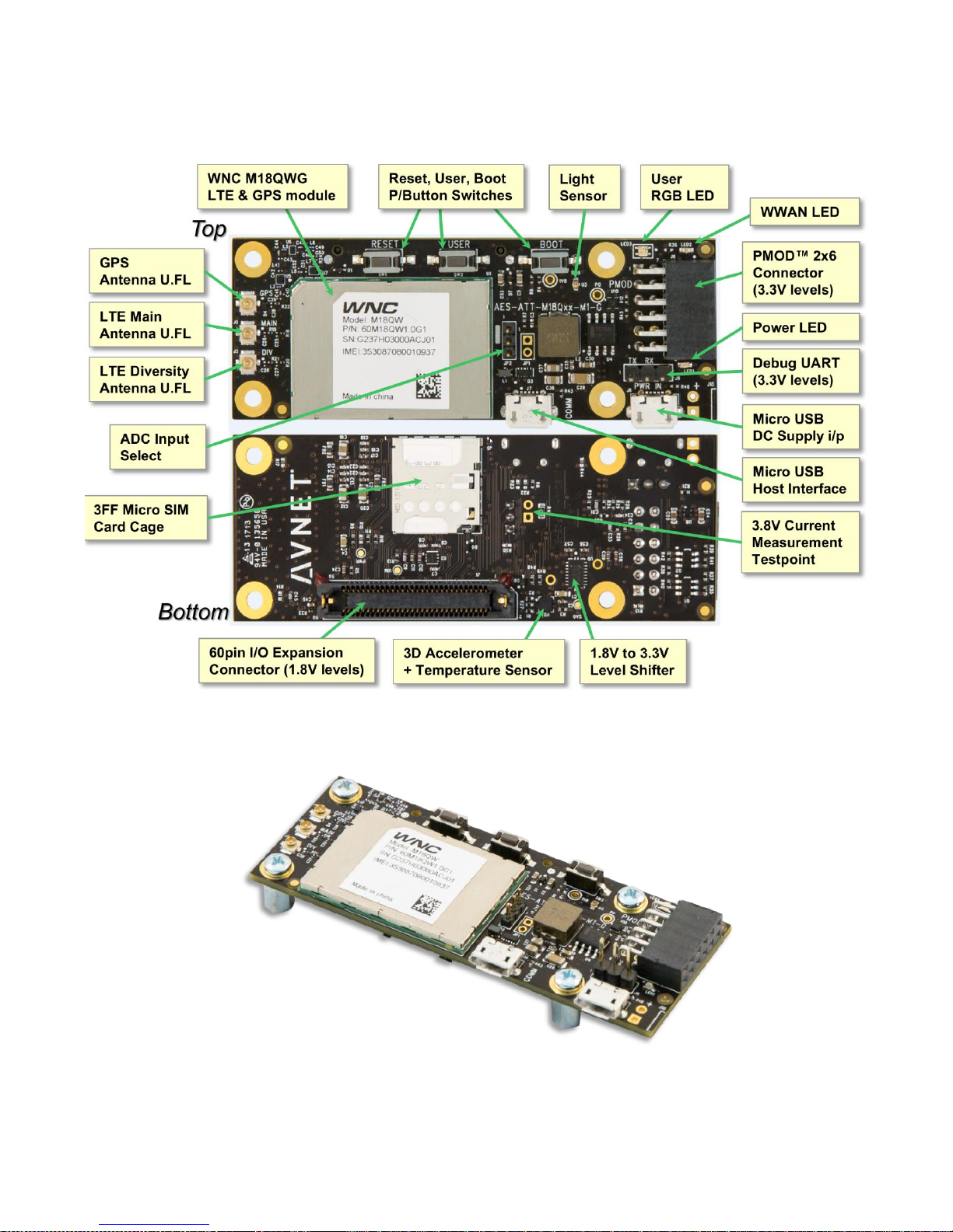
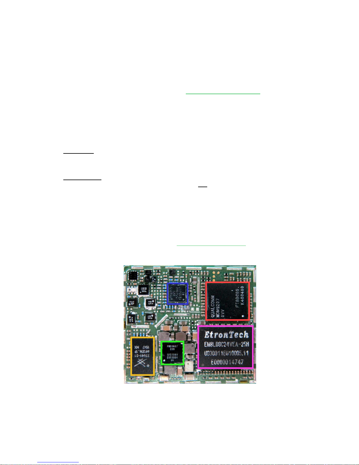
2.3 Location of Key Components
Figure 3 – LTE IoT System Board – Feature Identification
Figure 4 – Global LTE Cat.4 IoT System Board
Page 14
Page 14
3 LTE System Board Functional Description
The following sections describe the key functional blocks on the AT&T LTE IoT System Board
3.1 LTE Modem Module (WNC M18QWG)
The M18QWG is a SoC modem module from Wistron NeWeb Corporation (WNC) that provides
Cat.4 LTE cellular wireless connectivity plus GNSS location tracking, as well as a full-featured
application processor subsystem with peripheral interfaces and functions uniquely designed to
address the power/performance/cost constraints of IoT and M2M applications.
The quad-core ARM Cortex A7 applications processor on this module is based on Qualcomm’s
MDM9207 architecture and offers (OFDMA-related) software based signal processing capabilities
that significantly exceeds the efficiency of traditional ARM based communications processors.
Host mode: The WNC module will normally operate in “host mode”, where one of the ARM
Cortex A7 cores in the on-module Qualcomm MDM device is reserved for use as the system
processor for user applications. (The other three A7 cores are dedicated to the modem functions).
Modem mode: WNC module operation in “slave mode” (as a peripheral to an external processor
interfaced to the WNC module via USB interface) is not currently supported
The M18QWG also provides system peripheral interfaces and library support for these,
(eg. USB 2.0, I2C, SPI, SGMII, PCM, HSIC, UIM, UART*, SDIO*)
Refer to the next section pinout listing of the 60 pin Expansion Connector (Samtec ERF8) for
detail regarding the M18QWG module I/O that is accessible to the User
Documentation for the M18Q2 series WNC North America module that shares similar functionality
is available at the FCC certification website https://fccid.io/NKRM18Q2
Figure 5 – Internal view of the similar WNC M18Q2 series module
Page 15
Page 15
Figure 6 – Use Cases for Avnet LTE IoT Boards
…
Page 16
Page 16
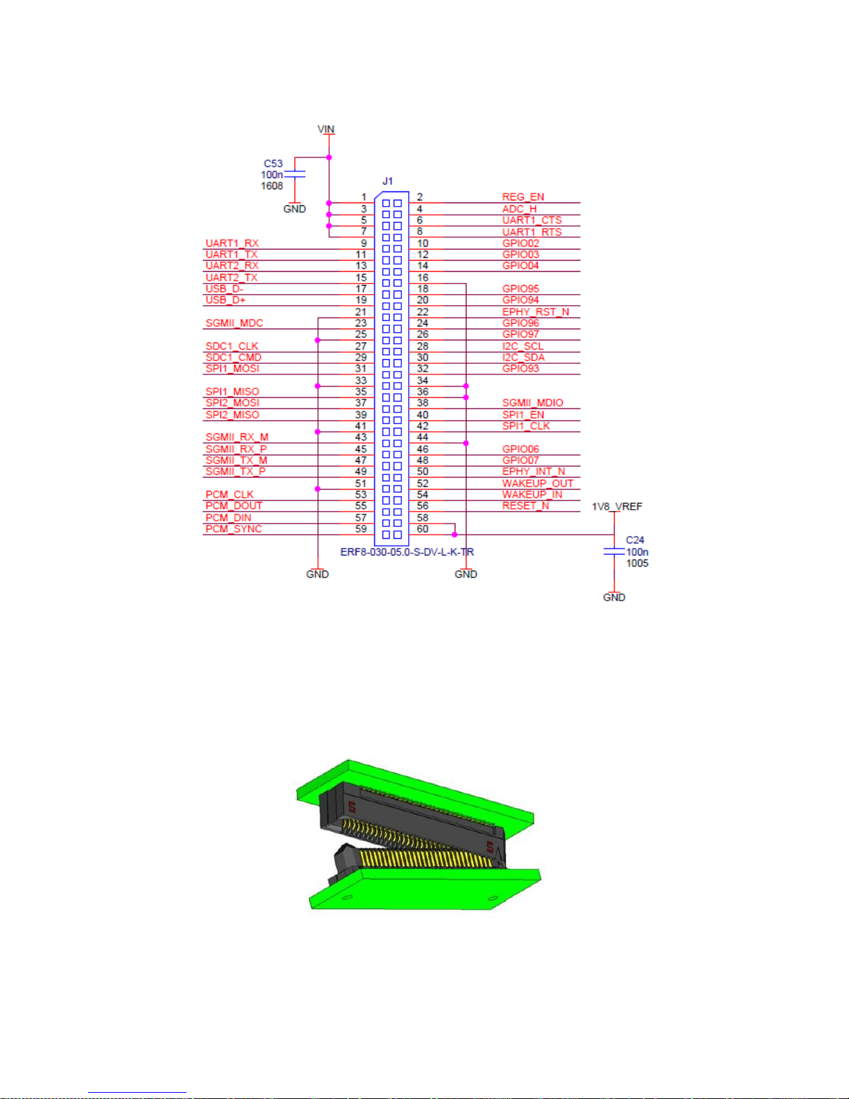
3.2 Expansion Connector
The peripheral interfaces of the WNC M18QWG module are made available to the developer for
custom system design via the board’s 60 pin Expansion Connector.
This is interface is implemented using a 2x30 pin, 0.8mm pitch, Samtec ERF8 series connector,
providing a robust, space-efficient and economical stacking solution that is especially attractive for
cases where small overall physical size of the final product is vital.
Figure 7 – 3D View of Samtec ERF8 / ERM8 Connector Pair
Page 17

Page 17
The matching Samtec ERM8 connector that is fitted to the custom end product PCB, is made
Manuf.
Avnet P/N
Description
Samtec
ASP⁃197278⁃01
ERM8 series connector to match ERF8 socket
(7 mm mated connector height)
Samtec
ASP⁃197278⁃02
ERM8 series connector to match ERF8 socket
(10 mm mated connector height)
Samtec
ASP⁃197278⁃04
ERM8 series connector to match ERF8 socket
(14 mm mated connector height)
available in three different stacking heights, to better accommodate height clearance requirements
of your custom hardware. These offer 7mm, 10mm or 14mm overall clearance between the boards
Figure 8 – Expansion Connector Polarization
Figure 9 – Expansion Connector Board Stack Profile-View
Page 18

Page 18
Table 2 – J1 Expansion Connector Pinout (Inner Row)
J1
pin
PCB Signal
Name
Description
WNC
pin
PU
/PD
WNC
Modem Mode
WNC
Host Mode
1
VIN
DC Input Voltage (5V)
-
-
-
3
VIN
DC Input Voltage (5V)
-
-
-
5
VIN
DC Input Voltage (5V)
-
-
-
7
VIN
DC Input Voltage (5V)
-
-
-
9
UART1_RX
Receive for WNC UART1
82
PD
UART1_RX
UART1_RX
11
UART1_TX
Transmit for WNC UART1
83
PD
UART1_TX
UART1_TX
13
UART2_RX
Receive for WNC UART2
106
PD
UART2_RX
UART2_RX
15
UART2_TX
Transmit for WNC UART2
107
PD
UART2_TX
UART2_TX
17
USB_D-
USB Data Negative
88 USB_DN
USB_DN
19
USB_D+
USB Data Positive
86 USB_DP
USB_DP
21
GND
GND
-
-
-
23
SGMII_MDC
SGMII Management
data clock
120
- SGMII_MDC
25
GND
GND
-
-
-
27
SDC1_CLK
SDC1 Clock
124
- SDC1_CLK
29
SDC1_CMD
SDC1 Command
123
- SDC1_CMD
31
SPI1_MOSI
SPI1 MOSI / SDC1_DATA3
125
PD
SPI1_MOSI
SPI1_MOSI
33
GND
GND
-
-
-
35
SPI1_MISO
SPI1 MISO / SDC1_DATA2
126
PD
SPI1_MISO
SPI1_MISO
37
SPI2_MOSI
SPI2 MOSI
62
PD - SPI2_MOSI
39
SPI2_MISO
SPI2 MISO
63
PD - SPI2_MISO
41
GND
GND
-
-
-
43
SGMII_RX_M
SGMII receive – minus
59
- SGMII_RX_M
45
SGMII_RX_P
SGMII receive – plus
58
- SGMII_RX_P
47
SGMII_TX_M
SGMII transmit – minus
57
- SGMII_TX_M
49
SGMII_TX_P
SGMII transmit – plus
56
- SGMII_TX_P
51
GND
GND
-
-
-
53
PCM_CLK
PCM Clock
49
PD
PCM_CLK/GPIO49
PCM_CLK/GPIO49
55
PCM_DOUT
PCM Data Out
48
PD
PCM_DOUT/GPIO48
PCM_DOUT/GPIO48
57
PCM_DIN
PCM Data In
47
PD
PCM_DIN/GPIO47
PCM_DIN/GPIO47
59
PCM_SYNC
PCM Sync
46
PD
PCM_SYNC/GPIO46
PCM_SYNC/GPIO46
PD: Pull-Down
PU: Pull-Up
NP: Non-Pull
Page 19

Page 19
Table 3 – J1 Expansion Connector Pinout (Outer Row)
J1
pin
Signal Name
Description
WNC
pin
PU
/PD
WNC
Modem Mode
WNC
Host Mode
2
REG_EN
3V8 Regulator Enable
-
PD - -
4
ADC_H
ADC ext. input (to JP2)
122
PD
ADC (via JP2)
ADC (via JP2)
6
UART1_CTS
CTS for WNC UART1
80
PD
UART1_CTS
UART1_CTS
8
UART1_RTS
RTS for WNC UART1
81
PD
UART1_RTS
UART1_RTS
10
GPIO02
GPIO02
53
PD
GPIO02
GPIO02
12
GPIO03
GPIO03
54
PD
GPIO03
GPIO03
14
GPIO04
GPIO04
55
PD
GPIO04
GPIO04
16
GND
GND
- -
-
18
GPIO95
GPIO95
95
PD
GPIO95
GPIO95
20
GPIO94
GPIO94
94
PD
GPIO94
GPIO94
22
EPHY_RST_N
EPHY_RST_N
103
PD - EPHY_RST_N
24
GPIO96
GPIO96
96
PD
GPIO96
GPIO96
26
GPIO97
GPIO97
97
PD
GPIO97
GPIO97
28
I2C_SCL
I2C_SCL
61
PD
I2C_SCL
I2C_SCL
30
I2C_SDA
I2C_SDA
60
PD
I2C_SDA
I2C_SDA
32
GPIO93
GPIO93 (output only)
93
NP
GPIO93
GPIO93
34
GND
GND - - -
36
GND
GND - - -
38
SGMII_MDIO
SGMII MDIO
121 -
SGMII_MDIO
40
SPI1_EN
SPI1 Enable / SDC1_DATA1
127
PD
SPI1_EN
SPI1_EN
42
SPI1_CLK
SPI1 Clock / SDC1_DATA0
128
PD
SPI1_CLK
SPI1_CLK
44
GND
GND - - -
46
GPIO06
GPIO06
130
PD
GPIO06
GPIO06
48
GPIO07
GPIO07
131
PU
GPIO07
GPIO07
50
EPHY_INT_N
EPHY_INT_N
132
PD
GPIO08
EPHY_INT_N
/ GPIO08
52
WAKEUP_OUT
WAKEUP_OUT
143
PD
WAKEUP_OUT
WAKEUP_OUT
54
WAKEUP_IN
WAKEUP_IN
144
PD
WAKEUP_IN
WAKEUP_IN
56
RESET_N
RESET_N
145
PD
RESET_N
RESET_N
58
1V8_VREF
WNC 1.8V LDO Output
146
VREF
VREF
60
1V8_VREF
WNC 1.8V LDO Output
146
VREF
VREF
PD: Pull-Down
PU: Pull-Up
NP: Non-Pull
Page 20

Page 20
Figure 10 – Expansion Connector Pin Numbering
Page 21

Page 21
Pmod
Pin#
Function
Signal Name
Pmod
Pin#
Function
Signal Name
1
SPI_SS
SPI1_EN_3V3
7
SPI_INT
GPIO93_3V3
2
SPI_MOSI
SPI1_MOSI_3V3
8
RESET
GPIO95_3V3
3
SPI_MISO
SPI1_MISO_3V3
9
I2C_SCL
I2C_SCL_3V3
4
SPI_SCK
SPI1_CLK_3V3
10
I2C_SDA
I2C_SDA_3V3
5
GND
GND
11
GND
GND
6
3V3
3V3
12
3V3
3V3
3.3 2x6 Pin Peripheral Connector
The 2x6 Pin Peripheral Connector is compatible with a subset of Pmod™ peripheral boards from
Digilent, Maxim, Measurement Specialties (TE Connectivity) and others.
The pinout of this 2x6 pin right-angle socket connector is derived from the I/O signal assignments
defined in the Digilent Pmod™ Interface Specification for SPI and I2C serial interfaces.
Note however, that dual-row I2C Pmod peripheral boards in many cases may not be fitted to this
board, as their duplicate SCL and SDA pins are not accommodated by the combo SPI plus I2C
interface pinout assignments implemented on the LTE System board.
Table 4 – 2x6 Pmod Peripheral Connector Pinout
Figure 11 – 2x6 Peripheral Connector Board Edge-View
Page 22

Page 22
3.4 WNC Module Interfaces
WNC
Pin #
WNC Module
Pin Name
WNC I/O
Direction
Avnet SOM
Signal Name
I/O Voltage
Levels
Signal
Description
133
UIM_VCC
AO
VCC_UIM_SIM
1.8V / 3.0V
SIM card power
134
UIM_DATA
DI/DO
UIM_SIM_IO
1.8V / 3.0V
SIM card data
135
UIM_CLK
DO
UIM_SIM_CLK
1.8V / 3.0V
SIM card clock
136
UIM_RESET
DO
UIM_SIM_RST
1.8V / 3.0V
SIM card reset
136
UIM_DETECT
DI/DO
UIM_SIM_DETECT
1.8V / 3.0V
SIM card detect
3.4.1 SIM Interface (3FF Micro-SIM Connector)
The UIM (User Identity Module) interface is implemented with a Micro-SIM connector that
interfaces a removable 3FF sized AT&T SIM card to the WNC module.
- This SIM interface includes the necessary ESD protection devices
- It is powered from the WNC module and will auto set to 1.8V or 3.0V upon SIM negotiation.
The UIM_DETECT input pin of the M18QWG module is driven from the UIM connector
circuit:
- If SIM card is present, UIM_DETECT = High (1.8V / 3.0V)
- If SIM card is absent , UIM_DETECT = Low (GND)
Table 5 – SIM Card Interface Connections
Notes:
- Power to the System board must be turned-off when removing or inserting the SIM card!
- The SIM card connector is not spring-loaded. To remove the SIM:
Turn the board upside-down. Eject the SIM by pushing from inside, outward to board-edge
Page 23

Page 23
3.4.2 USB Interface
WNC
Pin #
WNC Module
Pin Name
WNC I/O
Direction
Avnet SOM
Signal Name
Description
86
USB_DP
DI/DO
USB_D+
USB 2.0 Data Positive
87
USB Detect
DI
GPIO87
USB Detect
88
USB_DN
DI/DO
USB_D-
USB 2.0 Data Negative
The M18QWG module supports USB 2.0 high-speed protocol, it’s USB I/O lines complying
with the USB 2.0 electrical specification.
Table 6 – WNC USB Interface Connections
The USB electrical interface includes ESD protection and is accessible via either:
the MicroUSB connector, or
the 60-pin Expansion connector
The USB interface on the WNC module’s Qualcomm MDM9207 series quad-core processor
implements a “USB Compound Device” (Qualcomm-patented) with virtual USB hub enabling
multiple logical devices to enumerate over single physical USB interface.
When the LTE System board is first connected to the developer’s computer, it enumerates as
this USB peripheral device, implementing a total of 9 logical interfaces as shown in the
Windows screenshot on the next page…
Page 24

Page 24
Figure 12 – USB Interface Drivers Enumerate on Windows Host Computer
#
Description
Device this
Enumerates as
Windows
Device Drivers
Comments
1
WNC M18Q2 USB
Composite Device
qcusbfilter.sys,
usbqccgp.sys
2
CDC ECM
N/A
N/A
Installs on Linux host,
not Windows
3
WNC M18Q2
HS-USB Diagnostics
COM port
qcserv.sys
Serial over USB
4
WNC Composite
ADB Interface
Android device
WdfCoInstaller01009.sys,
WinUSBCoInstaller2.sys,
winusb.sys,
Android Debug Bridge
5
WNC M18Q2
HS-USB Android Modem
COM port
(modem)
qcserv.sys, modem.sys
Serial over USB, AT
Command interface
6
WNC M18Q2
HS-USB NMEA
COM port
qcserv.sys
Serial over USB,
GPS interface
7
WNC M18Q2
HS-USB Ethernet Adaptor
Network adaptor
qcusbwwan.sys
Ethernet over USB
for HS data transfer
8
USB Mass Storage Device
Removable disk
usbstor.sys
Virtual removable drive
9
Linux File-Stor Gadget
USB Device
Disk drive
disk.sys, iaStorF.sys,
partmgr.sys
Virtual disk drive
Table 7 – USB Logical Interfaces Reported by Windows Device Manager
The M18QWG module supports 3GPP standard AT commands and proprietary AT commands
For Linux based user software applications, the SDK supports API access via the MAL Manager
Page 25

Page 25
3.4.3 UART1 Interface
J9 Pin
Signal Name
Description
1
UART2_TX_3V3
Level-shifted WNC UART2_TX output
2
UART2_RX_3V3
Level-shifted WNC UART2_RX input
3
GND
Ground
The WNC module firmware limits UART1 to a predefined system function specifically for:
“High Speed Data Transfer”
WNC UART1 modem interface as implemented via the USB Compound Device, is available through either:
the MicroUSB connector, or
the 60-pin Expansion connector
As tabled on the previous page, additional UARTs (in service of the other processor cores) also
communicate over the same USB interface
3.4.4 UART2 – Software Debug UART Interface (3-pin header)
WNC UART2 is limited by the module firmware to performing the predefined system function of:
“Software Debug UART”
The I/O levels of this UART are level-shifted, with it’s TX, RX and GND signals made available on a
3-pin header (J9) to facilitate external connection to a 3rd-party USB-to-Serial debug cable
Table 8 – Software Debug UART Header (J9)
Page 26

Page 26
3.4.5 Voltage Level Translation (1.8V / 3.3V)
SPI1 and UART2 interfaces plus two GPIOs (GPIO93 and GPIO95) from the WNC module are
level-shifted to 3.3V levels by Fairchild FXLA108BQX octal bi-directional level-translator device
In addition, the I2C peripheral interface bus from the WNC module is also level-shifted, using
an FXMA2102L8X 2-bit level-translator that is compatible for use with open-collector outputs
The level-shifted 3.3V signals are routed to the following connectors:
the Pmod-compatible 2x6 peripheral connector (J8) and
the Software Debug UART 3-pin header connector (J9)
Page 27

Page 27
3.4.6 ADC / Ambient Light Sensor (JP2)
JP2 Pins
Signal Source for ADC Input
1 & 2 (default)
Ambient Light Sensor output (U3)
2 & 3
Expansion Connector (J1 pin 4)
(ie. driven by an external circuit)
A single ADC input is provided on the WNC module.
This inputs to a 16 bit convertor, sampled at 2.4MHz for an ENOB of 15 bits
Analog Input Bandwidth is 100 kHz (typical)
The ADC’s input range is 0.1V to 1.7V
A shorting link across jumper JP2 connects one of the following sources to this ADC input:
Table 9 – ADC Input Source Selector (JP2)
Note! Two issues should be noted that limit the utility of the ADC input on the initial production boards:
a) ADC input source selection via JP2 is not possible unless the R50 “default” resistor is removed
b) The ADC’s input voltage limit could be exceeded if the Ambient Light Sensor is exposed to an
excessively bright light source, resulting in potential damage to the module. To prevent this, it is
recommended that light-levels must be restricted using some form of optical filter placed over the
U3 light sensor (see U3 location below)
Figure 13 – Board Detail Showing Light Sensor (U3)
Page 28

Page 28
3.4.7 3D Accelerometer Sensor (LIS2DW12)
LIS2DW12 Pin Name
WNC Pin Name
Isolating Resistor
INT1
GPIO06
R48
INT2
GPIO07
R49
The LIS2DW12 is a 2017-released, ultra low-power, MEMS 3-axis smart accelerometer from
ST Micro. It has 16-bit output and can be configured (with 5 settings in either mode) to prioritize:
ultra-low power consumption (< 1 µA @ ODR = 12.5 Hz), or
very low-noise performance (down to 90 µg/√Hz)
Other features include:
Selectable acceleration full-scale range of ±2/±4/±8/±16 g
32-level embedded FIFO (for measurement buffering)
Thermal stability over the full -40 to +85 °C industrial temperature range
Embedded temperature sensor
1.8V operation and I/O levels
50 nA power-down mode
Dedicated internal engine for motion
and acceleration processing:
o Free-fall wakeup
o 6D/4D orientation
o Tap and double-tap recognition
o Activity/inactivity recognition
o Portrait/landscape detection
The LIS2DW12 is used as a slave device (address=0011001 b7) on the WNC module’s I2C
peripheral bus. The SA0 input of the LIS2DW12 device is tied high, but this signal is pinnedout to test-point SA0 to facilitate potential modification of (LSB) of the device I2C address
Table 10 – LIS2DW12 Interrupt Outputs
Both interrupt outputs are by default connected to the WNC module (GPIO06 and GPIO07)
If one or both of these WNC GPIOs are required for a different purpose, they may be
disconnected from the LIS2DW12 device by removing resistors R48 and R49
Page 29

Page 29
3.4.8 Pushbutton Switches (Reset, User, Boot)
Switch #
Name
Switch Function
How Activated
SW1
RESET
WNC module Reset input
Press and hold for > 3 seconds to Reset
SW2
USER
User-defined trigger input
User defined function, forces a logic Low on GPIO98
SW3
BOOT
Force USB Boot
Press + hold during reset, forces reprogramming of
firmware from USB (Note! This is an advanced
function that requires use of WNC_Dloader software)
Three pushbutton switches connected to inputs on the WNC module, are mounted on the most
mechanically secure section of the board (ie. pressing down on the 60-way expansion connector)
Table 11 – Pushbutton Switch Functions
Page 30

Page 30
3.4.9 LED Status Indicators (Power, WWAN, User)
LED #
Name
LED Function
How Activated
LED1
POWER
3V8 Power Good Indicator
Illuminates if board is powered
LED2
WWAN
Network Connection Status
Controlled by User software:
Indicates valid network connection
LED3
USER
User defined RGB output
Controlled by User software:
User defined color and sequence
Three LEDs are visible on the LTE System board, their functions are tabled below:
Table 12 – LED Indicator Functions
Page 31

Page 31
3.4.10 PCM / I2S Digital Audio Interface
PCM mode
I2S mode
WNC GPIO Pin
PCM_SYNC
I2S_WS
GPIO46
PCM_DIN
I2S_DATA0
GPIO47
PCM_DOUT
I2S_DATA1
GPIO48
PCM_CLK
I2S_SCK
GPIO49
PCM and I2S share the same four pins on the M18QWG module.
ie. The Digital Audio interface pins can be configured for PCM or I2S functionality.
These four pins can alternatively serve as user-defined GPIO, see table below…
Access to these signals is via the 60-pin Expansion Connector
Note: Software support for the Digital Audio Interface is not currentltly included in the SDK
Figure 14 – CODEC Interface Using PCM or I2S
Table 13 – PCM / I2S Digital Audio Interface Pins
Page 32

Page 32
3.4.11 Ethernet SGMII Interface
An SGMII interfaced Ethernet MAC is integrated within the WNC module.
This has the following key features
IEEE 802.3 compliance
Full duplex at 1 Gbps
Half/full duplex for 10/100 Mbps
Supports VLAN tagging
Supports IEEE 1588, Precision Time Protocol (PTP)
Can be used connected to an external Ethernet PHY such as AR8033,
or to an external switch
Layout recommendations:
Differential impedance:100 Ω
Space to other signals: > 3x line width
Lane-to-lane space: > 3x line width
Intra-lane mismatch: < 0.7 mm
Page 33

Page 33
3.4.12 User GPIO
GPIO
Name
J1
Pin #
Host Mode Function
/ Also Connects To…
PU
/PD
Comments
GPIO02
10
PD GPIO03
12
PD
GPIO04
14
PD
GPIO06
46
LIS2DW12: INT1 (*Note1)
PD
To use as GPIO, disable INT1
GPIO07
48
LIS2DW12: INT2 (*Note1)
PU
To use as GPIO, disable INT2
GPIO08
50
EPHY_INT_N
PD
Available as GPIO if SGMII not used
GPIO46
59
PCM Sync (*Note2)
PD
Level-shifted on LTE IOT Carrier board
GPIO47
57
PCM Data In (*Note2)
PD
Level-shifted on LTE IOT Carrier board
GPIO48
55
PCM Data Out (*Note2)
PD
Level-shifted on LTE IOT Carrier board
GPIO49
53
PCM Clock (*Note2)
PD
Level-shifted on LTE IOT Carrier board
GPIO93
32
PMOD: J8 pin 7 (*Note1)
NP
Level-shifted on Pmod Interface
GPIO94
20
PD GPIO95
18
PMOD: J8 pin 8 (*Note1)
PD
Level-shifted on Pmod Interface
GPIO96
24
PD GPIO97
26
PD GPIO120
23
SGMII_MDC (*Note3)
PD
Check WNC firmware support
GPIO123
27
SDC1_CMD (*Note3)
PD
Check WNC firmware support
GPIO124
29
SDC1_CLK (*Note3)
NP
Check WNC firmware support
Signal
Name
J1
Pin #
Assigned Function
On Avnet Board
Comments
GPIO92
n/a
RGB LED: Red
User controlled RGB LED (Red)
GPIO98
n/a
User P/B Switch
User controlled Pushbutton Switch
GPIO101
n/a
RGB LED: Green
User controlled RGB LED (Green)
GPIO102
n/a
RGB LED: Blue
User controlled RGB LED (Blue)
Eighteen of the signals routed from WNC module to the Expansion Connector (J1) can operate
as GPIO serviced by the User Application software (see comments regarding use):
Table 14 – GPIO Signals Available on Expansion Connector
*Note1 Take care to avoid contention if GPIO shared with other devices or interfaces
*Note2 PCM Digital Audio pins are configured as GPIO in current WNC Host mode firmware
*Note3 Check GPIO 120, 123, 124 support in the version of WNC firmware used
PU = Internal Pull-Up resistor, PD = Internal Pull-Down resistor, NP = Output Only
Table 15 – GPIO Signals Assigned Local Functions
Page 34

Page 34
3.5 Power Regulation
Voltage Rail
Voltage
Current max (A)
VIN
5.0V (nominal)
1.8 A (MicroUSB)
4.0 A (Exp. Connector)
3V8 (VCC)
3.8V
3.0 A
1V8_VREF (VREF)
1.8V
0.1 A
VCC_UIM_SIM
1.8V / 3.3V
0.15 A
3V3
3.3V
0.3 A
Table 16 – Summary of LTE System Board Voltages
3.5.1 VIN
Unregulated DC input power (in range of 4.5V to 16V) can be supplied to the LTE System
board via one of three different input interfaces:
the “PWR IN” MicroUSB connector (J6)
the 60-pin Expansion Connector (J1)
the 2-pin VIN and GND aux connector (J10, unpopulated)
In the IoT Starter Kit, the provided 5V 2.5A AC/DC power adaptor applies power to the LTE
System board via the “PWR IN” MicroUSB (J6) connector
The input supply voltage can be measured by placing voltmeter test leads across the
unpopulated DC aux input connector pads (J10)
3.5.2 3V8 (VCC)
3.8V @ 3 A max, An onboard ON Semi NCP3170 buck switching regulator supplies the WNC
module’s VCC input requirement. Regulators on the WNC module then convert this voltage
down to the lower core voltages required
The REG_EN regulator enable input:
is pulled high following power-up via an RC delay circuit (enables the 3V8 output)
can be pulled low from the 60-pin Expansion Connector (to disable the 3V8 output)
Power Good status of the 3V8 output supply rail can be verified in two places
LED1 - illuminates green when the circuit is correctly powered and REG_EN is high
PG test point - this should be high (when circuit is powered and REG_EN = high)
An unpopulated 2-pin header site (JP1) is provided for 3V8 current measurement.
To use this feature, the following board modification is required:
Zero-ohm resistor R47 must be removed
A 2-pin header connector JP1 must be added
The meter test leads must be placed across the pins of JP1
After completion of current measurements, a shorting link (JPR1) must be fitted
across these JP1 header pins
Page 35

Page 35
Page 36

Page 36
The 3V8 module supply is filtered per WNC recommendations using the following circuit
3.5.3 1V8_VREF (VREF)
1.8V @ 100 mA max. Supplied by the VREF pin of the WNC module.
This provides 1.8V power to the following circuits:
The VREFA input of the 1.8V/3.3V level-shifter devices (U9 and U10)
The LIS2DW12 accelerometer
The LNA in the GNSS/GPS antenna circuit
Some discrete pull-up resistors
3.5.4 VCC_UIM_SIM (UIM_VCC)
1.8V or 3.0V @ 150mA max. Supplied by the UIM_VCC output pin of the WNC module
This voltage is auto set on SIM negotiation and provides 1.8V or 3.3V power to:
The “User Identity Module”, ie. the removable SIM Card.
3.5.5 3V3
3.3V @ 150 mA max. Supplied by the onboard On Semi NCP114 LDO regulator.
This supplies 3.3V power to the following circuits:
The VREFB input of the 1.8V/3.3V level-shifter devices (U9 and U10)
The Pmod Interface (J8)
Page 37

Page 37
Signal Name
Connected to
I/O
Function in this Circuit
RESET
J1 pin 56
IO
Allows expansion board to reset the WNC module
WAKEUP_IN
J1 pin 54
I
Allows expansion board to wake-up WNC module
WAKEUP_OUT
J1 pin 52
O
WNC module wake-up output to expansion board
REG_EN
J1 pin 2
I
3V8 Regulator Enable
POWER_ON
PWR testpoint
I
Unused, but available at “PWR” test-point
WWAN_STATE
WWAN LED
O
Drives network status WWAN LED (Amber color)
Under program control from the User application
Function
Driven by
Signal Name
WAKEUP_IN = Low
Host
Host allows Modem to sleep
WAKEUP_IN = High
Host
Host requires the Modem, or this an ACK
response to a WakeUp from the Modem
WAKEUP_OUT = Low
Modem
Modem allows the Host to sleep
WAKEUP_OUT = High
Modem
Modem requires the Host, or this an ACK
response to a WakeUp from the Host
3.7 WNC Module Power Control and State Interfaces
The following 6 signals fall in this category:
Table 17 – Control and State Signals
RESET
The RESET signal on the 60-pin Expansion Connector may be used as an input or output. This
functions in parallel with the onboard SW1 pushbutton switch. The WNC module is reset by a logic
low on this signal for 3 seconds or longer
WAKEUP_IN and WAKEUP_OUT
For power-sensitive applications, this mechanism allows the modem and an external host to enter
low power states whenever possible, with the other side then waking it when required.
If the modem receives data while the host is in low power state, then it must wake-up the host.
If the host needs to transmit data while the modem is in low power state, then the host must be
able to wake-up the modem.
The interface consists of two signals:
WAKEUP_IN is driven by an external host and received by the modem
WAKEUP_OUT is driven by the modem and received by the host.
Each side can wake the other side by toggling it’s wakeup signal high, or
allowing the other side to go to sleep when not needed by toggling wakeup low.
Table 18 – WAKEUP_IN and WAKEUP_OUT
Page 38

Page 38
REG_EN and POWER_ON
REG_EN controls the main 3V8 regulator and is pulled high (enabled) following power-up via an
onboard RC delay circuit. This signal is also available on the 60-pin Expansion Connector for
external ON/OFF control of the onboard 3V8 and 3V3 regulators. This allows system power to be
controlled by eg. a low-power MCU on the User’s custom hardware
Figure 15 – Sleep and Power Control of WNC Module
POWER_ON is the power control input to the WNC module. This is made available on a test-point
(“PWR”) but is otherwise unused in this design. (Not available on the 60-pin Expansion Connector)
Note: In the event the User application also needs control of the POWER_ON input, this requires
rework of the LTE System board as R11 will need to be removed
WWAN_STATE
This signal drives the WWAN LED (Amber color) and is normally used to indicate network status,
but is control from the User application so can be repurposed if necessary
Page 39

Page 39
3.8 Antennas
Manuf.
Part Number
Description
Antenna Circuits
Pulse
W6113B0100
FPC combo 3-in-1 antenna
LTE + GPS + LTE
Pulse
W3906B0100
W3907B0100
FPC dual antenna
FPC single antenna
LTE + GPS
LTE
Pulse
W3907B0100
W3908B0100
2x FPC single antennas
1x FPC GPS antenna
LTE, LTE
GPS
3.8.1 LTE Antennas (Primary, Diversity)
This IoT Starter Kit ships with it’s three antennas implemented on two FPC antenna
assemblies (see 2nd option highlighted in bold type below)
Avnet’s antenna partner Pulse provide three different implementation options using FPC type
antennas, for maximum flexibility in achieving specific end-product form-factors
Table 19 – FPC Antenna Options from Pulse
Features of these Pulse FPC antennas include the following:
2G / 3G / 4G MIMO
Global LTE bands: B1-B23, B25-B29, B33-B42 (N.America, Europe, Asia incl.Japan)
Guaranteed Port-to-Port isolation
Foldable for tight spaces
2.9 dBi gain for LTE antennas
0.3 or 0.8 dBi dBi gain for GNSS antenna
Figure 16 – Detail of U.FL Antenna Connectors
Page 40

Page 40
3.8.2 GPS Antenna
GPS and adaptive A-GPS are supported by the WNC module
The GNSS antenna circuit is made up of the following circuitry:
SAW filters 1 and 2 : Murata SAFFB1G56KB0F0AR15
Low Noise Amplifier: Infineon BGA824N6
The LNA device is enabled under firmware control, by GPIO05 on the WNC module
Figure 17 – GPS Antenna Circuit Diagram
The GPS antenna section of the LTE System board schematic is detailed on the next page…
Page 41

Page 41
Page 42

Page 42
4 Specifications and Ratings
Parameter
Min
Typ
Max
Unit
VIN (DC Supply Voltage)
4.5
5.0
16
Volts
MicroUSB connector VIN rating @5V
1.8
A
Expansion connector VIN rating @5V
4.5
A
3V8 Voltage Regulator rating
3.0
A
3V3 Voltage Regulator rating
300
mA
Parameter
Min
Typ
Max
Unit
V_High on WNC Digital I/O
1.7
1.8
1.9
Volts
Voltage on WNC ADC Input
0 1.7
Volts
Parameter
Test Condition
Typ
Unit
Airplane mode
Module only (no other device)
0.86
mA
LTE Standby mode lowest power
consumption (Band 8)
DRX=2.56 sec, BW=10MHz
1.01
mA
LTE Standby mode highest power
consumption (Band 2)
DRX=2.56 sec, BW=10MHz
1.22
mA
LTE Working mode lowest power
consumption (Band 40)
BW=20MHz, PTX =23dbm, DL=145Mbps
400
mA
LTE Working mode highest power
consumption (Band 7)
BW=20MHz, PTX =23dbm, DL=145Mbps
800
mA
WCDMA standby mode lowest
power consumption (Band 8)
DRX=2.56 sec
0.98
mA
WCDMA standby mode highest
power consumption (Band 5)
DRX=2.56 sec
1.06
mA
WCDMA Working mode lowest
power consumption (Band 8)
HSPA+ DL=21 Mbps, PTX =23 dBm
389
mA
WCDMA Working mode highest
power consumption (Band 2)
HSPA+ DL=21 Mbps, PTX =23 dBm
433
mA
4.1 Absolute Maximum Ratings
Table 20 – Absolute Maximum Ratings
4.2 Recommended Electrical Operating Conditions
Table 21 – Recommended Electrical Operating Conditions
4.3 Power Consumption
Typical power consumption @ Vcc = 3.8V
(Note! WNC module only consumption, from WNC M18QWG specifications)
Table 22 – Power Consumption
Page 43

Page 43
GSM standby mode lowest
power consumption (GSM850)
DRX=1.18 sec
1.12
mA
GSM standby mode highest
power consumption (GSM1900)
DRX=1.18 sec
1.18
mA
GSM Working mode lowest
power consumption (GSM1800)
GPRS 1 down 4 up, TX Power=33dbm
751
mA
GSM Working mode lowest
power consumption (GSM900)
GPRS 1 down 4 up, TX Power=33dbm
913
mA
Powering On Consumption
Power consumption peak when module
is powering up
780
mA
Power Off Consumption
Power when module is powered off
10
uA
Parameter
Typical
Unit
TX Power (LTE)
23.0
dBm
TX Power (WCDMA)
23.5
dBm
TX Power (GSM)
32.5 / 29.5
dBm
RX Sensitivity (LTE)
-99 to -102
dBm
RX Sensitivity (WCDMA)
-108.5 to -110
dBm
RX Sensitivity (GSM)
-107 to -109
dBm
Parameter
Characteristics
Notes
Carrier and Technology
4G LTE Cat.4
WCDMA
GSM
Supported Bands: LTE Cat.4
B1/3/7/8/20/28/38/40
3GPP release 10
(no Carrier Aggregation)
Supported Bands: WCDMA
B1/8
3GPP release 8
Supported Bands: GSM
E-GSM 900, DCS 1800
VoLTE (Voice over LTE)
Yes
Security
(See White Paper 1Q18)
Data Rates (LTE Cat.4)
150/50 Mbps for DL/UL
4.4 RF Characteristics
Table 23 – TX Power and RX Sensitivity
4.5 Networking and Carrier
Table 24 – Networking and Carrier Characteristics (Europe Operation)
Page 44

Page 44
4.6 GNSS Receiver Performance
Test Items
Parameter
Typ
Unit
Cold start TTFF
@ -130 dBm
38
Seconds
Hot start TTFF
@ -130 dBm
2
Seconds
CEP-50 Accuracy
Open sky with -130 dBm input
< 3
Meters
Cold start sensitivity
Acquire First with Signal level
-146
dBm
Tracking sensitivity (GPS)
Detect an in-view satellite
50% of the time
-162
dBm
Parameter
Min
Typ
Max
Unit
Humidity Range*
%
Storage Temperature
-40 +85
ºC
Operating Temperature**
- LTE System Board Functional
- WNC Module Functional
- WNC Module 3GPP Compliant
-25
-25
-20
+60
+75
+60
ºC
* Non-condensing, relative humidity
** Thermal spec for push-button switches is -40 to +60C
Table 25 – GNSS receiver performance
4.7 Environmental
Table 26 – Environmental Characteristics
Page 45

Page 45
4.8 Mechanical
Parameter
Characteristics
LTE System board PCBA dimensions
29.5 mm × 30 mm × 10 mm (typ.)
Table 27 – Mechanical Characteristics
Figure 18 – Mechanical Details (1 of 2)
Page 46

Page 46
Page 47

Page 47
5 Certifications
Manuf.
Part Number
Description
Antenna Circuits
Pulse
W3906B0100
W3907B0100
FPC dual antenna
FPC single antenna
LTE + GPS
LTE
5.1 RoHS Compliance
The AES-ATT-M18QWG-M1-G module is lead-free and RoHS compliant.
5.2 Regulatory and Network Certifications
End-device certification testing has been completed and test reports submitted for CE-RED Approval. The
scope of this CE-RED certification covers the Global LTE Starter Kit using the specified Pulse antennas
and power supply that ships in this kit.
5.2.1 Certification Documents
Certification-CE_RE_Directive_Examination_Certificate_AES-ATT-M18QWG-SK-G
Certification-CE_DoC_AES-ATT-M18QWG-SK-G
5.2.2 CE-RED: EMC Testing
Additional EMC testing will be required when this module is:
a) fitted to an additional PCB assembly, and/or
b) the external power supply is changed
5.2.3 CE-RED: Radio Testing
CE certification testing of this kit was conducted with the LTE SOM board fitted with the Pulse
antennas tabled below. Use of different antennas will require additional certification testing!
Table 28 – Certified Pulse Antennas
5.2.4 Electrical Safety Certification
Due to the small form-factor of the LTE SOM board, the details below are provided in this
Hardware User Guide to fulfil the regulatory requirement to display the CE mark, brand name,
model number and electrical rating
Page 48

Page 48
6 Shipping, Handling and Storage
6.1 Shipping
Bulk orders of AES-ATT-M18QWG-M1-G LTE System boards are delivered in trays of TBD units.
6.2 Handling
The AES-ATT-M18QWG-M1-G LTE System board contains sensitive electronic circuitry that
requires proper ESD protection when handling. Failure to follow these ESD procedures may
result in permanent damage to the module.
The module should not be subjected to excessive mechanical shock.
6.3 Storage
Per J-STD-033, the shelf life of devices in a Moisture Barrier Bag is:
12 months at <40ºC and <90% room humidity (RH).
Do not store in salty air or an environment where there is a high concentration of corrosive gas,
such as Cl2, H2S, NH3, SO2, or NOX.
Do not store in direct sunlight.
7 Safety Recommendations
Be sure the use of this product is authorised for use in the country and environment where is operated.
The use of this product may be hazardous and must be avoided in areas:
Where it can interfere with other electronic devices, eg in hospitals, airports and aircraft
Where there is a risk of explosion such as gasoline stations and oil refineries
It is the responsibility of the user to comply with their country’s regulations and environmental regulations.
Do not disassemble the product; any mark of tampering will compromise the warranty’s validity.
It is recommended the instructions in this hardware user guide be followed for correct wiring of the product.
The product must be supplied with a reliable voltage source, and wiring must conform to the security and
fire-prevention regulations.
This product must be handled with care; avoid contact the possibility of electrostatic discharge which may
damage the product. Same caution must be taken regarding the UIM card; carefully check the instructions
for its use. Do not insert or remove the UIM when the product is in power-saving mode.
The system integrator is responsible for the functioning of the final product. Care must be taken with the
circuitry external to the module as well as for project or installation issues—there may be a risk of disturbing
the cellular network or external devices or of having an impact on device security. If you have any doubts,
please refer to the technical documentation and the relevant regulations in force.
Every module must be equipped with a proper antenna of the specified characteristics. The antenna must
be installed with care in order to avoid any interference with other electronic devices.
Page 49

Page 49
8 Ordering Information
Part Number
Description
MSRP
AES-ATT-M18QWG-SK-G
AT&T LTE Cat.4 IoT Starter Kit
$139.00
AES-ATT-M18QWG-M1-G
AT&T LTE Cat.4 IoT System Board
$99.00
Manuf.
Avnet Part Number
Description
MSRP
Samtec
ASP⁃197278⁃01
ERM8 series matching connector
(7 mm mated connector height)
$1.35
Samtec
ASP⁃197278⁃02
ERM8 series matching connector
(10 mm mated connector height)
$1.35
Samtec
ASP⁃197278⁃04
ERM8 series matching connector
(14 mm mated connector height)
$1.90
Manuf.
Part Number
Description
Antenna Circuits
MSRP
Pulse
W6113B0100
FPC combo 3-in-1 antenna
LTE + GPS + LTE
Pulse
W3906B0100
W3907B0100
FPC dual antenna
FPC single antenna
LTE + GPS
LTE
Pulse
W3907B0100
W3908B0100
2x FPC single antennas
1x FPC GPS antenna
LTE, LTE
GPS
Table 29 – Ordering Information
8.1 LTE System Board Accessories
8.1.1 Expansion Connector Options for Custom User Board
System Designers have a choice of three different stack heights, for overall inter-board
clearances of 7mm, 10mm or 14mm
Table 30 – Height options for Samtec ERM8 Expansion Connector
8.1.2 Pulse FPC Antenna Options
Pulse has providioned three different implementation options using FPC type antennas, for
maximum flexibility in achieving specific end-product form-factors
Table 31 – FPC Antenna Options from Pulse
The highlighted 2nd option shows the antennas that ship in the IoT Starter Kit.
(This is the pair of antennas covered in the certification)
Page 50

Page 50
Figure 19 – Pulse FPC Antenna Options
Page 51

Page 51
9 Contact Information
Region
Email
General Global Kit Enquiries
eval.kits@avnet.com
Europe Sales Enquiries
ebvchips@ebv.com
For further details, contact your local Avnet representative or e-mail us at:
Table 32 – Contact Information
10 Technical Support
Technical support for the Global LTE IoT Kit is available via online support forum pages.
These are located (on same website as the product documentation) at:
http://cloudconnectkits.org/forum
11 Disclaimer
Avnet assumes no liability for modifications that the owner chooses to make to their LTE IoT Starter Kit
Page 52

Page 52
12 Appendix A – LTE IoT Breakout Carrier
The LTE IoT Breakout Carrier is an optional expansion board that facilitates system-level prototyping
using the Global LTE IoT Starter Kit
Via it’s Samtec ERM8 series 60-pin connector, a subset of the WNC LTE module’s peripheral interfaces
(signaling at 1.8V levels) are level-shifted to 3.3V levels and pinned-out to two Click Module sockets for
which over 300 different MikroElekronika Click peripheral modules are available for purchase from Avnet.
Features:
Access to key peripheral interfaces of LTE System Module via 60 pin Samtec ERM8 series
connector (10mm mated connector height. 10mm standoffs required for mounting of LTE Board)
Level-shifting of the WNC module signals to/from 1.8V / 3.3V levels
Dual sockets for two MikroE Click peripheral modules (available from Avnet)
Flexible system prototyping via a choice of over 425 Click peripheral modules
External control of LTE System board power-down and sleep modes
Additional level-shifted GPIO (or PCM Digital Audio) signals (four pins)
Onboard 3.3V and 1.8V voltage regulators
Figure 20 – LTE IoT Breakout Carrier (plus Click Modules)
LTE IoT Breakout Carrier details and ordering info available at:
http://cloudconnectkits.org/product/lte-iot-breakout-carrier
 Loading...