

Page 1

t
N
E
Avidyne DVX-740/750 VHF Nav/Com
Module Installation & Initial Checkou
AVIDY
CORPORATION
55 Old Bedford Road
Lincoln, MA 01773
and
420 N. Wickham Rd, Suite B
Melbourne, FL 32935
Document Number 610-00060-xxx Control Category CC2
Revision Description ECO Date
00 Release for FCC testing 6/15/2006 DCO-06-104 06/13/06
01 Revised per FCC Timco review 10/03/2006 DCO-06-211 10/09/06
Confidential property of Avidyne Corporation
Not to be disclosed without permission
Page 2

DVX-740/750 VHF Nav/Com Installation & Checkout Manual
Table of Contents
1. Scope and Purpose............................................................... 3
2. Configuration of the DVX-750 Module................................. 3
3. Specification of the DVX-750 Module.................................. 5
3.1 - FAA Certification Objectives............................................................................................7
TSO Applicability..............................................................................................................7
Environmental Category................................................................................................... 8
Computer Software ..........................................................................................................9
Hardware Assurance........................................................................................................9
3.2 - FCC Certification Objectives............................................................................................9
4. Circuit Description and Theory of Operation ................... 10
5. Initial Checkout and Test Procedure................................. 17
6. Glossary............................................................................... 21
Confidential property of Avidyne Corporation 610-00060Not to be disclosed without permission Revision: -01 Date:10/09/2006
Page 2 of 21
Page 3
DVX-740/750 VHF Nav/Com Installation & Checkout Manual
1. Scope and Purpose
The purpose of this manual is to verify functionality of the DVX-750 VHF Nav/Com
radio before installation into a host PFD chassis. End user operation of the DVX-750 is
defined by the user I/O devices and displays that are provided by the host chassis.
Therefore, this is not a “User’s Manual” for the end user (customer), but provides some
direction for those who need to operate the DVX-750 module “stand-alone” during
development, certification, production, or repair activities.
2. Configuration of the DVX-740/750 Module
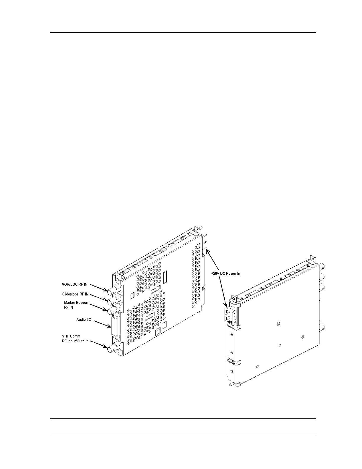
The DVX-750 top level module, Part# 710-00060-( ), consists of metal and mechanical
parts as captured in the top level part as well as the following internal boards:
a. RF Board, 320-00116-( )
b. DSP Board, 320-00115-( )
The DVX-740 is the same module but with the Marker Beacon receiver disabled on the
RF Board. There are no changes to the Digital Board. The BNC connector for the
Marker Beacon receiver is installed, so the external connection of the module thru the
rear panel of the chassis is the same with either configuration.
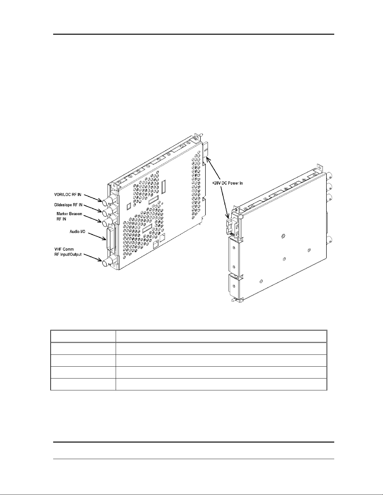
Fig 1.1 – DVX-740/750 VHF Nav/Com Module.
Confidential property of Avidyne Corporation 610-00060Not to be disclosed without permission Revision: -01 Date:10/09/2006
Page 3 of 21
Page 4
DVX-740/750 VHF Nav/Com Installation & Checkout Manual
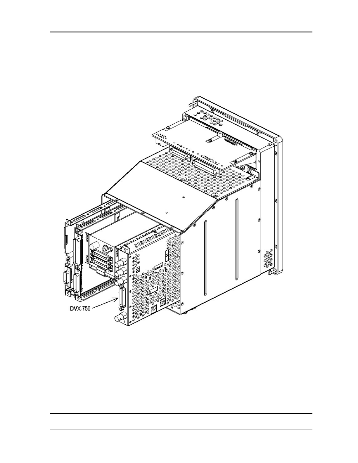
The assembled DVX-750 slides into the host chassis, engaging the 60-pin backplane
connector which provides power and ground connections as well as the Byteflight data
interface for control (input) and data output. Installation steps are simply seating the
unit in the cardguides and ensuring that the backplane connector is engaged, then
tightening the Allen head retainer screws. After the rear panel is installed on the
chassis the BNC retainer nuts with star washers must be installed.
Figure 1.2 – DVX-750 Module installed in a Primary Flight Display (Chassis shown is
Avidyne Part#, 700-00078-000).
Confidential property of Avidyne Corporation 610-00060Not to be disclosed without permission Revision: -01 Date:10/09/2006
Page 4 of 21
Page 5
DVX-740/750 VHF Nav/Com Installation & Checkout Manual
3. Specification of the DVX-740/750 Module
The DVX-750 VHF radio module operates as an airborne VHF COMM transceiver
allowing a flight crew to aurally communicate with Air Traffic Control (ATC), other
ground stations, or different aircraft in the VHF aeronautical band. It also operates as
an airborne ILS/VOR receiver for radio aided navigation and guidance. The DVX-750
must be hosted by a PFD (Primary Flight Display) chassis, which provides conditioned
DC power and digital interface to control radio functions.
In ILS mode the VHF radio estimates own aircraft horizontal and vertical deviation
from the selected ILS localizer and glide paths. In VOR mode it estimates own aircraft
bearing to the selected VOR ground station relative to magnetic north (at the station).
In addition, any speech or identification audio signals are presented aurally to the flight
crew.
The DVX-750 radio can also operate as an airborne Marker Beacon receiver and
provides some Audio Panel functionality allowing it to interface to headsets
(microphone and headphones), a cabin speaker and a transmitter key without requiring
and audio panel.
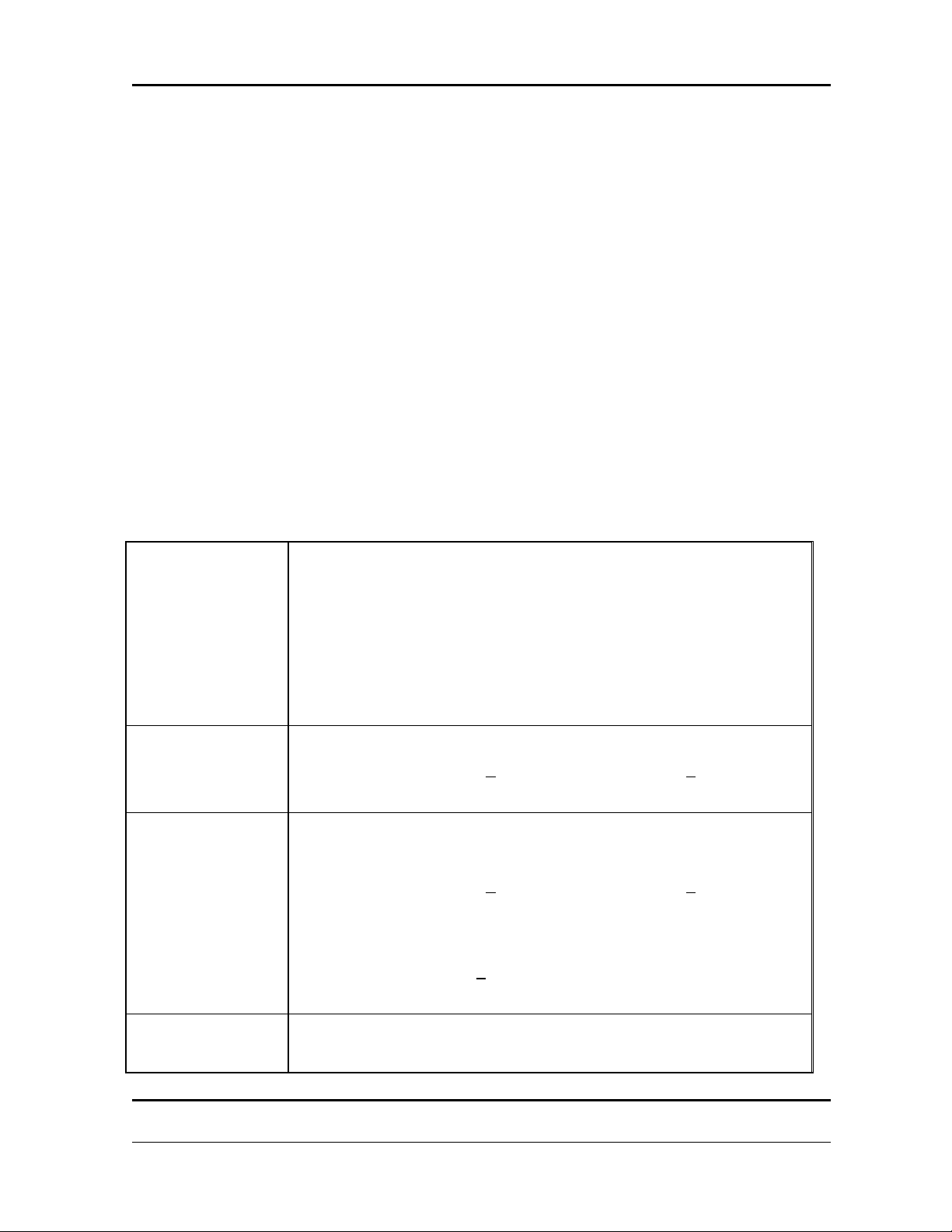
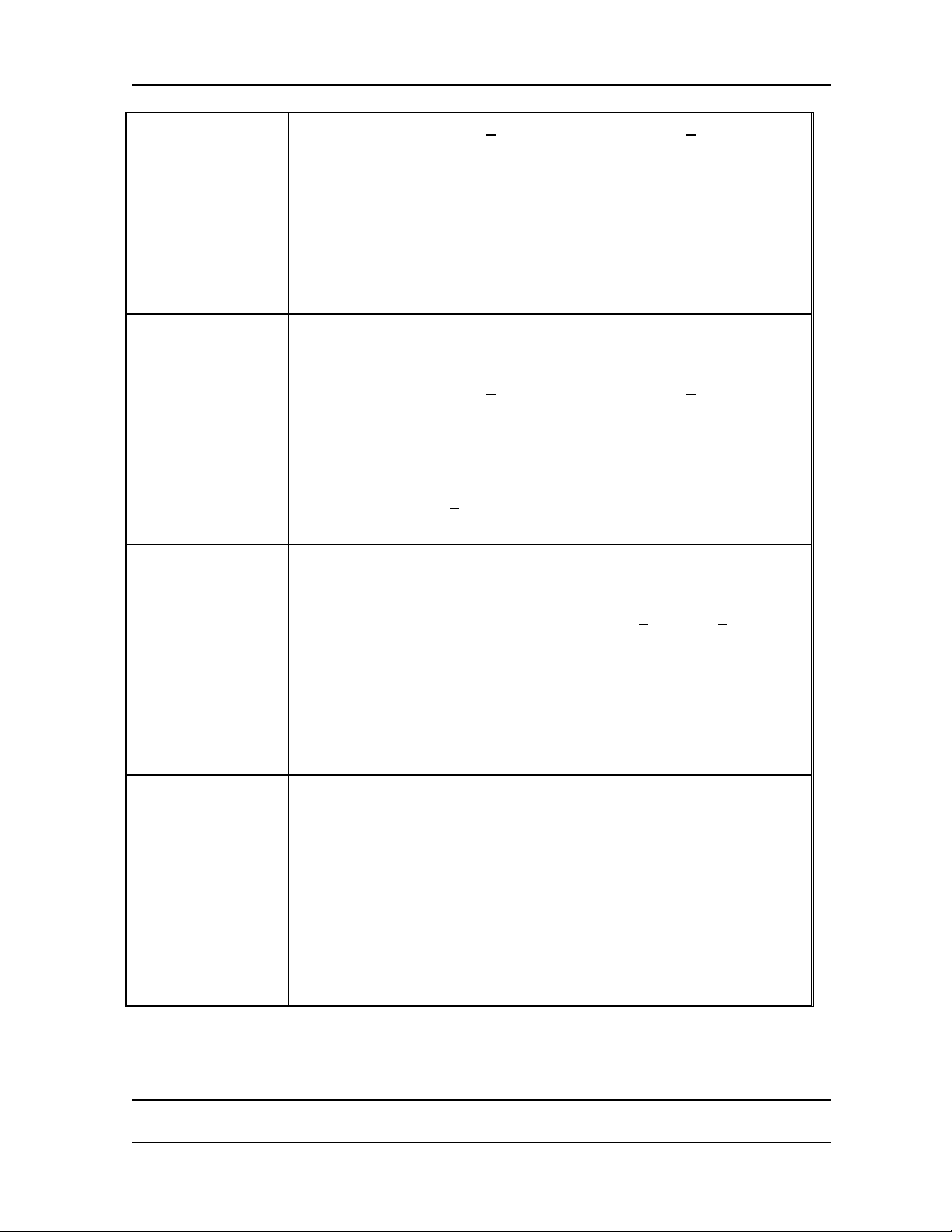
Table 3-1. VHF Radio Characteristics Summary
Audio System 6 microphone or line in
5 headphone or line out
1 speaker out
Headphone outputs: 35mW into 150 ohm <1% THD,
65mW into 150 ohm <10% THD
Speaker output: 8W into 4 ohms
-Frequency response: 300 to 6000Hz within 6dB
Marker Beacon
Receiver
(optional)
Glideslope
Receiver
Operating frequency: 75MHz
Selectivity: 6dB at least
Sensitivity (high): 200uV (factory default)
Operating frequency: 328.60 to 335.40 MHz
Channel # / spacing: 40 channels at 150 kHz spacing
Selectivity: 6dB at least
Sensitivity (flag): 36uV max
Spurious response: -60dB or better
Centering accuracy: 0
Defection response: 67% of final value in 600msec
+10 kHz, 40dB no more than +200 kHz
+21 kHz, 40dB no more than +160 kHz
+0.02 DDM or better
Localizer Rcvr Operating frequency: 108.00 to 112.00 MHz
Channel # / spacing: 40 channels at 50 kHz spacing
Confidential property of Avidyne Corporation 610-00060Not to be disclosed without permission Revision: -01 Date:10/09/2006
Page 5 of 21
Page 6
DVX-740/750 VHF Nav/Com Installation & Checkout Manual
Selectivity: 6dB at least
Sensitivity (flag): 10uV max
Sensitivity (aural): 10uV max for 20dB (s+n)/n with 1kHz 30% mod
Spurious response: -60dB or better
Centering accuracy: 0
Deflection response: 67% of final value in 600msec
Audio response: 350 to 2500Hz <6dB, <20dB at <150Hz, >9kHz
VOR Receiver Operating frequency: 108.00 to 117.95 MHz
Channel # / spacing: 160 channels at 50 kHz spacing
Selectivity: 6dB at least
Sensitivity (flag): 5uV max
Sensitivity (aural): 5uV max for 6dB (s+n)/n with 1kHz 30% mod
Spurious response: -60dB or better
Bearing accuracy:
Audio response: 350 to 2500Hz <6dB, <20dB at <150Hz, >9kHz
VHF COMM
Digital Receiver
Operating frequency: 118.000 to 137.975 MHz
Channel # / spacing: 760/2280 channels at 25/8.33 kHz spacing
+17 kHz, 40dB no more than +80 kHz
+0.007 DDM or better
+17 kHz, 40dB no more than +80 kHz
+2.0 degrees or better
VHF COMM
Analog
Transmitter
Selectivity (8.33/25kHz): -40dB no more than
Sensitivity: 2uV max for 6dB (s+n)/n with 1kHz 30% mod
Spurious response: (S+N)/N is > 6dB for 10mV spurious signal
AGC Characteristics: <6dB audio variation from 10uV to 10mV
Squelch: Automatic with carrier override
Audio response: 350 to 2500Hz within 6dB, down 18dB at 4kHz
Frequency Range : 118.000 – 136.992
Carrier Power Output: 16W minimum, 18W typical
Emission Type: dual sideband AM, Emission Designator – 6K00A3E
DC Power to Final Amplifier: 3A @ 28V = 84W
Duty cycle: 25% (30sec transmit, 90 sec receive)
Spurious content: -60dBc or better
Modulation capability: 70% minimum, 80% limiting
Modulation Fidelity: 350 to 2500 Hz within 6dB, <20% THD
+7.37kHz /+25 kHz
Confidential property of Avidyne Corporation 610-00060Not to be disclosed without permission Revision: -01 Date:10/09/2006
Page 6 of 21
Page 7
DVX-740/750 VHF Nav/Com Installation & Checkout Manual
3.1 - FAA Certification Objectives
The VHF radio module will be developed such that the hosting integrated avionics product can
be installed and certified in Part 23, Class I, II, and III aircraft via STC or TC modification. To
achieve this end, the equipment will be certified at the equipment level via the TSO process. This
process plus the additional certification objects for this product are summarized below.
(1) FAA airworthiness approvals - This includes detailed performance and environmental
testing, as well as some additional susceptibility tests. These tests are discussed in detail in the
following sections. The FAA issues Technical Standard Orders (TSO's) that refer to the relevant
RTCA (Radio Technical Commission for Aeronautics) specifications. The RTCA documents in
turn refer to ISO (International Standards Organization), ARINC (Aviation Radio Incorporated),
and ICAO (International Civil Aviation Organization) documents.
(2) Derived functionality - Additional features not covered in the FAA standards must also be
tested (such as channel scanning, back-end interfaces, speech intelligibility enhancements, and
other value-added features).
(3) European approvals - EUROCAE (European Organization for Civil Aviation Electronics)
were allowed to comment and contribute to the RTCA documents, so there are few distinctions
to achieve European certification. One notable exception is the extended frequency coverage of
the VHF DSB-AM up to 156 MHz (which is not a part of this radio's specification).
TSO Applicability
The VHF radio, when installed in the host integrated avionics product, shall comply with the
minimum performance standards defined by the following technical standard orders (TSO):
Table 3-2. VHF Radio Required TSO Objectives
TSO
Number
TSO-C34e ILS Glide Slope Receiving Equipment Operating within the Radio
Frequency Range of 328.6-335.4 Megahertz (MHz)
TSO-C36e Airborne ILS Localizer Receiving Equipment Operating within the Radio
Frequency Range of 108-112 Megahertz (MHz)
TSO-C40c VOR Receiving Equipment Operating within the Radio Frequency Range
of 108-117.95 Megahertz (MHz)
TSO-C128 Devices that prevent blocked channels used in two-way radio
communications due to unintentional transmissions
TSO-C169 VHF Radio Communications Transceiver Equipment Operating Within
the Radio Frequency Range 117.975 to 137.000 Megahertz
The following TSOs are optional:
Table 3-3. VHF Radio Optional TSO Objectives
Subject Title
TSO No. Subject Title
TSO-C35d Airborne Radio Marker Receiving Equipment
Confidential property of Avidyne Corporation 610-00060Not to be disclosed without permission Revision: -01 Date:10/09/2006
Page 7 of 21
Page 8
DVX-740/750 VHF Nav/Com Installation & Checkout Manual
TSO-C50c Audio Selector Panels and Amplifiers
Environmental Category
The VHF radio, when installed in the host integrated avionics product, shall meet the following
requirements of DO-160E while being operated.
Table 3-4 VHF Radio Environmental Categories
Conditions Section Test Categories
Temperature and Altitude
Low Temperature
High Temperature
In-Flight Loss of Cooling
Altitude
Decompression
Overpressure
Temperature Variation 5.0 Category C, except conduct 10 cycles
Humidity 6.0 Category A
Shock and Crash Safety 7.0 Category B, aircraft type 3, test type F
Vibration 8.0 Category S, and Zone 1, curves C and M
Explosion 9.0 Not applicable
Waterproofness 10.0 Category W
Fluids Susceptibility 11.0 Not applicable
Sand and Dust 12.0 Not applicable
Fungus 13.0 Category F. This requirement may be met
Salt Spray 14.0 Not applicable
4.0
4.5.1
4.5.2, 4.5.3
4.5.4
4.6.1
4.6.2
4.6.3
Category A1
Category A1
Category A1
Category V
Category A1
Category A1, to 41000 feet
Category A1
by an analysis of unit materials
Magnetic Effect 15.0 Category A
Power Input 16.0 Category Z and MIL-STD-70E, section
5.3.3.1, 5.3.3.3, 4.3b
Voltage Spike 17.0 Category A
Audio Frequency Susceptibility 18.0 Category B
Induced Signal Susceptibility 19.0 Category Z
Radio Frequency Susceptibility 20.0 Category W
Radio Frequency Emission 21.0 Category M
Lighting Induced Transient 22.0 Change 3, Category A4J44
Lighting Direct Effects 23.0 Not applicable
Icing 24.0 Not applicable
Confidential property of Avidyne Corporation 610-00060Not to be disclosed without permission Revision: -01 Date:10/09/2006
Page 8 of 21
Page 9
DVX-740/750 VHF Nav/Com Installation & Checkout Manual
Conditions Section Test Categories
Electrostatic Discharge 25.0 Category A
Other Tests Fire resistance tests in accordance with
FAR Part 25, Appendix F.
Computer Software
The VHF radio software components shall be verified and validated to Level B per the process
described in RTCA/DO-178B.
Hardware Assurance
The VHF radio programmable hardware components shall be verified and validated to Level B
per the process described in RTCA/DO-254.
3.2 - FCC Certification Objectives
(1) FCC Part 15 certification - The FCC must approve the system for unintended emissions. This
will require that the radio functions be fully exercised during the execution of these tests. FCC
approvals must be received before FAA certification can be completed.
(2) FCC Part 87 certification - The FCC must approve the VHF communications transmitter
(spectral mask, modulation, power levels, etc.) before FAA testing may be completed.
The DVX-740/750 will be certified as a module such that it can be hosted by any compatible
FAA certified Primary Flight Display (PFD). Testing will be conducted in accordance with
Federal Communications Code of Federal Regulations, Part 2 Subpart J, including paragraphs
2.907, 2.911, 2.913, 2.915, 2.926, and 2.1031 through 2.1057, dated October 1, 2002. As well as Part
87, chapter D including paragraphs 87.131 through 87.147 and applicable paragraphs of Part 15.
Specific tests are listed in Table 3-5:
Table 3-5. VHF Radio FCC Certification Objectives
Test # Subject Title Reference Document
1 RF Power Output CFR 47, Para. 87.131
2 Modulation Characteristics CFR 47, Para. 87.141
3 Occupied Bandwidth of Emissions CFR 47, Para. 87.135
4 Limitations on Spurious Emissions CFR 47, Para. 87.139
5 Field Strength of Spurious Radiation CFR 47, Para. 2.1053, 2.1057, 15.209
6 Frequency Stability CFR 47, Para. 87.133
Confidential property of Avidyne Corporation 610-00060Not to be disclosed without permission Revision: -01 Date:10/09/2006
Page 9 of 21
Page 10

DVX-740/750 VHF Nav/Com Installation & Checkout Manual
4. Circuit Description and Theory of Operation
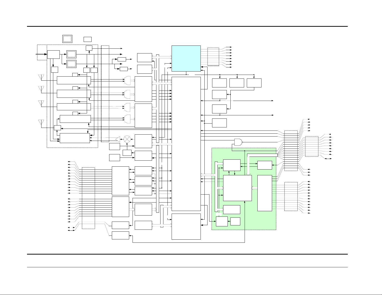
NOTE: Refer to Block Diagram (Fig 4.1) and circuit schematics during the following description.
The DVX-750 VHF radio module operates as an airborne VHF COMM transceiver allowing a
flight crew to aurally communicate with Air Traffic Control (ATC), other ground stations, or
different aircraft in the VHF aeronautical band. It also operates as an airborne ILS/VOR receiver for
radio aided navigation and guidance. The DVX-750 must be hosted by a PFD (Primary Flight
Display) chassis, which provides conditioned DC power and digital interface to control radio
functions.
The DVX-750 consists of two internal printed circuit boards, the “RF Board” (Part# 310-0011600x) and the “Digital Board” (Part# 310-00115-00x). The concept is to for analog signal processing to
occur on the RF board and digital processing to be performed on the Digital Board.
The choice was made to do the analog-to-digital conversions on the Digital board with carefully
matched analog differential signals interfacing between the two boards thru a 50-mil pitch stacking
connector. The transmitted signal is generated digitally and converted to analog on the Digital
board and sent to the RF board, while the received signals, which represent the entire operational
radio band for each receiver, are fed into the Digital board as differential analog signals and
immediately converted to digital format to be channelized and demodulated by the digital
downconverter and signal processor. While there can only be one transmitted signal at a time, there
can be as many as eight receivers operating simultaneously. Note that nothing changes on the RF
board when a receiver frequency is changed, since the entire radio band is fed into the Digital board.
The receivers are identified as:
Nav Rcvr – Tuned to condition and pass only the 108Mhz to 118Mhz Localizer and VOR
Navigation bands such that the digitizer on the Digital board can undersample the RF signal without
Nyquist alias signals appearing from out-of-band interference. The analog circuitry on the RF board
provides the necessary filtering of signals that would appear in the Nyquist bands, and it applies the
gain needed to optimize sensitivity based on signal strength of the in-band signals..
Glideslope Rcvr – Tuned to pass the 326 to 335 Mhz Glideslope signal band, it also provides
sufficient filtering to allow the digitizer to undersample the received RF without causing Nyquist
alias responses from out-of-band interference.
Marker Beacon Rcvr – Very tightly tuned to pass only a single channel at 75Mhz, this receiver
includes a custom crystal filter and also allows undersampling of the RF signal.
Comm Rcvr – Tuned to pass only the 118 to 137Mhz VHF aeronautical band, this receiver
interfaces to a T/R switch, allowing it to share the same antenna with the 16W Comm transmitter. It
also provides anti-aliasing filtering and optimizes gain for sensitivity without allowing signals to
overload the A/D converters doing the
Confidential property of Avidyne Corporation 610-00060Not to be disclosed without permission Revision: -01 Date:10/09/2006
Page 10 of 21
Page 11
DVX-740/750 VHF Nav/Com Installation & Checkout Manual
3.3V
Switcher Linear
Connector
+28V
FPSM
NAV Ant
G/S Ant
MB Ant
COM Ant
OV/UV
Protect
23V
T/R
SPEAKER
HP_LINE_1
HP_LINE_2
HP_LINE_3
HP_LINE_4
HP_LINE_5
MIC_LINE_1
MIC_LINE_2
MIC_LINE_3
MIC_LINE_4
MIC_LINE_5
MIC_LINE_6
DSCR_OUT_1
DSCR_OUT_2
TX_KEY_1
TX_KEY_2
TX_KEY_3
DSCR_IN_1
DSCR_IN_2
DSCR_IN_3
DSCR_IN_4
RS232_FPGA
RS232_BF
12V
3.3V
5V
LOC / VOR Rcvr
5V
Glide Slope Rcvr
5V
Markr Beacn Rcvr
5V
VHF COMM Rcvr
VHF COMM
Transmitter
RF Board
Connector
5V
7V
Audio
10V
RF
Connector
NV_ATTEN
GS_ATTEN
196M
XO
20M
TCXO
2.5V
1.6V
CM_ATTEN
Audio
Interface
Discrete
Interface
RS232
Transceiver
RS232
Transceiver
5V_DIG
12V_DIG
3.3V_DIG
A/D
A/D
A/D
A/D
VCO
FLASH
SRAM
NAV DDC
4 chan
COMM DDC
4 chan
DUC
PLL Synth
Audio
CODEC 1
Audio
CODEC 2
Audio
CODEC 3
Discrete
Input
Register
SRAM
Addr / Data
I2C
Addr / Data
SPI
SPI
SPI
Primary
Digital Signal
Processor
flash_page
nav_ch1
nav_ch2
nav_ch3
nav_ch4
com_ch1
com_ch2
com_ch3
com_ch4
TR_Enable
PA_Enable
cic_ovfl
iq_mod(14)
FPGA
tr_en
pdclk
lock_det
spi_tune
aud1_in
aud1_out
aud2_in
aud2_out
aud3_in
aud3_out
aud_mclk
rs232_rx
rs232_tx
disc_out
Auxiliary
Digital Signal
Processor
I2C
dsp1_reset_n
dsp1_int
dsp1_ardy
clk_49m
clk_57m
clk_ref
pa_mon
pa_pwr
tr_switch
pa_en
bf_eclk
bf_sys_reset_n
bf_clk_pull
dsp2_reset_n
dsp2_int
dsp2_ardy
Addr / Data
GPIO
49M
VCXO
57M
VCXO
20M
TCXO
40M
Cypress
Clock PLL
TXCLK_ENABLE
CODEC1_CSn
CODEC2_CSn
CODEC3_CSn
APA_MUTEn
DUC_RESETn
DDCC_RESETn
DDCN_RESETn
EEPROMEEPROM
CPLD
9S12 Data
Bus Processor
SRAM
10M
Clock
VCXO
Trim DAC
Byteflight
Data Bus
Controller
49M
57M
RS485
Transceiver
Voltage
Monitor
Interface
to NAV
A/D, DDC
to COMM
A/D, DDC
RF
Connector
Digital Card
Voltage
Monitors
PA_MON
PA_PWR
TR_SWITCH
PA_EN
LOAD_SHED_Bn
FPSM
Connector
28V_MON
26V_MON
RF_TEMP
12V_MON
10V_MON
5V_MON
3.3V_MON
2.5V_MON
1.6V_MON
DIGITAL_TEMP
ANLG_IN_0
ANLG_IN_1
ANLG_IN_2
ANLG_IN_4
HC912_VREF
Figure 4.1 – VHF Nav/Com Block Diagram
Confidential property of Avidyne Corporation 610-00060Not to be disclosed without permission Revision: -01 Date:10/09/2006
Page 11 of 21
Page 12

DVX-740/750 VHF Nav/Com Installation & Checkout Manual
Circuit Description by Functional Group (refer to the block diagram Figure 4.1):
1. Nav Receiver :
The Nav Receiver connects to a VOR/Localizer antenna via BNC connector J1 at the rear
of the DVX-750 module. For lightning protection the input signal is immediately bypassed
by gas-discharge tube G1 if the voltage exceeds 90V peak. The desired radio signal or any
remaining pulse from a lightning strike, passes thru a 2000V series DC blocking capacitor to
shunt choke L95, which shorts out any remaining remnant of a lightning strike without
significantly loading the desired radio signals.
Next the received signal is bandpass filtered (includes L2, L15, L26 etc) to reduce the level
of interference from the FM radio band (88Mhz to 108Mhz) before applying the signal to the
first stage LNA amplifier, U1. Just in front of the LNA is a PIN diode attenuator, D3, which
is autonomously activated when the RF monitor U22 senses an overload condition (e.g. when
an adjacent aircraft is transmitting). The FM rejection filter has a switchable high end notch,
which cuts the passband from 10Mhz to approximately 5Mhz when a VHF Comm
transmitter is keyed on the same aircraft. This avoids self-interference with Localizer
reception, which is especially critical during final approach.
After the LNA is a 6
provides more rejection of out-of-band interfering signals. Following this is a switchable
attenuator (U4, R13, R14, etc) providing either 0dB or 12dB attenuation which is switched in
when the A-to-D converter (U20) on the Digital board approaches an overload condition.
th
order LC bandpass filter (includes L10, L5, L23, L6, etc) which
The last two amplifier stages (U3 and U2) provide gain to enhance sensitivity and are
separated by a differential bandpass filter which further suppresses out-of-band interference.
The signal was converted from single ended (unbalanced) to balanced at transformer (T2)
just after the LNA, so the interface between the RF board and Digital board is a 200 ohm
differential pair transmission line. The differential pair is shielded by the six adjacent pins as
it passes thru stacking connector J5.
On the Digital board the signal is transformer coupled by T3, then passes thru a single
tuned LC stage (L5 and C68) providing some suppression of digital noise and clock signals.
U20 converts the analog signal to a 12-bit parallel data stream. The digital downconverter IC,
U12 provides carrier lock, channelization filtering and AGC, and AM demodulation and
audio formatting and mixing is performed digitally in DSP1, U19. Audio signals are routed
to the correct output channel via CODECs U42, U44 or U50 and associated output amplifiers
which convert the digital output to audio signals suitable for driving headphones, speakers
or other audio devices.
2. Glideslope Receiver :
The Glideslope Receiver connects to the Glideslope antenna via BNC connector J3 at the
rear of the DVX-750 module. The input signal is lightning protected by the same
combination of components used in the Nav receiver (see previous description), using a gasdischarge tube, 2000V series capacitor and RF choke to ground.
Next the received signal is bandpass filtered (L28, L32 and associated tuning capacitors)
to reduce the level of out-of-band interference before feeding the LNA. There is no provision
for adjusting front-end gain or damping signal overloads since nearby frequencies are not
generated on an aircraft.
Confidential property of Avidyne Corporation 610-00060Not to be disclosed without permission Revision: -01 Date:10/09/2006
Page 12 of 21
Page 13

DVX-740/750 VHF Nav/Com Installation & Checkout Manual
The LNA output feeds a SAW filter via LC matching elements. The SAW filter passband
is 315 to 335MHz which provides anti-alias filtering such that the digitizer can undersample
the RF signal without creating alias bands outside the Glideslope frequency band. The SAW
filter output is applied to transformer T5 to feed differential amplifier U5. Next a differential
filter (L98, L99, etc), and a 12dB gain step is applied before final amplification at U7 and
transmission to the Digital board via J5.
On the Digital board the signal is transformer coupled by T2, LC filtered by L4 and C67,
and A-to-D converted by U20. Processing by the DDC is nearly identical to the Nav receiver.
3. Marker Beacon Receiver:
The Marker Beacon signal is locally generated at 3miles, 1mile and ½ mile from the end
of the runway, and is always at 75MHz. The distance is indicated to the pilot by different
audio frequency tones which are AM modulated onto the 75MHz carrier.
The Marker Beacon Receiver connects to the Marker Beacon antenna via BNC connector J4 at
the rear of the DVX-750 module. The input signal is lightning protected by the same
combination of components used in the Nav and Glideslope receivers (see description in
section 1 above), using a gas-discharge tube, 2000V series capacitor and RF choke to ground.
Next the received signal is bandpass filtered (L34, L39 and associated tuning capacitors)
to reduce the level of out-of-band interference before feeding the LNA. Large signals are
handled by desensitizing the entire receiver, which shifts the available dynamic range high
enough to accommodate adjacent TV channels 4 & 5. The signal amplitude is dropped in R43
and R44 prior to the overload protection diode at D7 and the LNA, U11. There is no
switchable gain anywhere in the Marker Beacon receiver.
The output of the LNA feeds a crystal filter, FL3 which attenuates the strong TV signals
sufficiently to avoid overloading the ADC. A final filter (L35, C89, and C90) provide antialias filtering before the last amplifier U10 sends the signal to the Digital board via J5.
On the Digital board the signal is transformer coupled by T4, LC filtered by L9 and C109,
and A-to-D converted by U36. Processing by the DDC, U45 is nearly the same as for the
Glideslope receiver, and AM detection and audio output is performed by DSP1 and the
selected CODEC and audio output circuitry as described in section 1 above.
4. Comm Receiver :
The VHF Communication Receiver connects to the T/R switch (implemented with PIN
diodes D11, D12 and D13) which connects to a VHF antenna via BNC connector J6 and
allows the same antenna to be utilized for transmission or reception. See T/R switch
description.
The received signal is bandpass filtered (includes L60, L40, L62 etc) to reduce the level of
interference from the FM radio band (88Mhz to 108Mhz) before applying the signal to the
first stage LNA amplifier, U12. Just in front of the LNA is a PIN diode attenuator, D10,
which is autonomously activated when the RF monitor U31 senses an input overload. The
Comm receiver front-end is also contolled by the A/D converter (U37 on the Digital card) to
switch in 12 dB of attenuation (using R60 and D9) along with 12dB further along to produce a
24dB stepped attenuation to handle large in-band signals (or leakage of out-of-band signals).
After the LNA is a 6
th
order LC bandpass filter (includes L46, L43, L64, L44, etc) which
provides more rejection of out-of-band interfering signals. Following this is a switchable
Confidential property of Avidyne Corporation 610-00060Not to be disclosed without permission Revision: -01 Date:10/09/2006
Page 13 of 21
Page 14

DVX-740/750 VHF Nav/Com Installation & Checkout Manual
attenuator (U15, R64, R65, etc) providing either a 0dB or 12dB attenuation which is activated
at the same time as the front-end attenuator (using R60 and D9).
The last two amplifier stages (U14 and U13) provide gain to enhance sensitivity and are
separated by a differential bandpass filter (L47, L66, etc) which further suppresses out-ofband interference.
The signal was converted to a balanced differential signal at transformer (T10) just after
the first amplifier and continued to be processed as a differential signal from there on, so the
interface between the RF board and Digital board is a 200 ohm differential pair transmission
line. The differential pair is shielded by the six adjacent pins as it passes thru stacking
connector J5.
On the Digital board the signal is transformer coupled by T5, then passes thru a single
tuned LC stage (L10 and C110) providing some suppression of digital noise and clock signals.
U37 converts the analog signal to a 14-bit parallel data stream which feeds DDC, U45. the
DDC provides carrier lock, channelization filtering and AGC. AM demodulation and audio
formatting and mixing is performed digitally in DSP1, U19. Audio signals are routed to the
correct output channel via CODECs U42, U44 or U50 and associated output amplifiers which
convert the digital output to audio signals suitable for driving headphones, speakers or other
audio devices.
5. T/R Switch:
BNC connector J6 provides both input and output for the VHF Comm transceiver, and
therefore, use of the same antenna. When set to the “transmit” position, the nominal 16W
(55W peak) transmitter output is applied via PIN diode D13 and passes thru the transmitter
harmonic filter to the BNC, while the receiver is protected from the high voltage (150V peakto-peak) by L70 and by D12 shunting any leakage signal to ground. In the “receive” state
D13 is shut off, becoming a high impedance which keeps the PA from loading the input
signal. The series impedance of L70 is now cancelled by C196 forming a nominal 50-ohm
path between antenna input and the Comm receiver. The array of chokes and resistors
surrounding these components apply the correct DC bias to the PIN diodes to switch from
“receive” to “transmit” when discrete logic signal T_RN changes. Q6 and Q10 translate the
3Volt logic signal to the 24V drive signals used by the T/R switch.
6. Harmonic Output Filter
L83, L86, and associated capacitors form a VHF band (118 – 137 MHz) filter with L91
creating a notch in the frequency range where the 2
nd
harmonic falls. Above the 2nd
harmonic, the tuning provided by L83 and L86 is sufficient to suppress harmonic output of
the final amplifier. G4 is a gas-discharge tube with a 240V trigger voltage to clamp lightning
surge voltages to ground at the input BNC. The Bandpass nature of the harmonic
suppression filter is sufficient to attenuate the residual lightning surge allowed by the GDT
(i.e. 240V and more during activation of the GDT).
7. VHF Power Amplifier (PA):
The RF board receives a signal created on the Digital board by the Digital Upconverter
(DUC). The signal enters via J5 as a differential signal at about -1dBm and is transformer
coupled by T12. Transmitted signal level is adjusted by attenuator R75, R76, R77 and R81.
Clock noise, spurious DUC output, and digital noise is suppressed by a differential input
Confidential property of Avidyne Corporation 610-00060Not to be disclosed without permission Revision: -01 Date:10/09/2006
Page 14 of 21
Page 15

DVX-740/750 VHF Nav/Com Installation & Checkout Manual
filter (L67, L75/L76, L74/L82, etc) then a driver signal of approximately 200mW is generated
by U17 and U18. This differential signal is applied to the intermediate stage push-pull
amplifier Q5, a 40W RF MOSFET and then to Q4 which is a 90 Watt MOSFET device. Bias
voltage, “FET_BIAS” is switched off by Q13 when not transmitting and is applied to Q5 via
the coupling transformer and to Q4 via RF chokes. Inductors L90 and L87 along with C231,
C229, C227, C219 etc, provide impedance matching of the RF MOSFETs. The push-pull
output is coupled to the 50-ohm single-ended output by the rigid coaxial transformer T16.
8. Transmit signal generator:
The Digital Upconverter (DUC) U46 has a 48-bit internal direct digital synthesizer (DDS)
and an integrated 14-bit digital-to-analog converter, allowing it to output a differential
analog signal ready for amplification and transmission. The DUC is fed a digital audio
baseband via a 14-pin input bus, which is applied to the DDS output to create AM
modulation (i.e. it multiplies the carrier amplitude). The audio signal from the selected input
source (“MIC_LINE_1 to 6) is digitized in an audio CODEC and formatted for the DUC by
DSP1. The current-source output from the DUC is coupled and filtered (L18, L19, L14, L15,
L13 and associated capacitors), amplified by U38, then filtered (L601, L602 and associated
caps), amplified again at U601 then applied to mixer U641. The LO for the mixer comes from
a phase-locked loop synthesizer formed primarily by U630 and U602, then amplified at U640,
and filtered (L721, L723, L724 and associated caps). The DUC output is always at 53MHz,
while the synthesizer output varies from 171 to 190 MHz, thus producing the required range
of carrier frequencies of 118-137 MHz, which is Bandpass filtered (L695, L643, L691 etc) and
amplified to drive the connection to the RF board via J6.
Transmitter frequency stability and accuracy: TCXO Y64 provides a frequency stability of
1.5ppm for the PLL synthesizer, and XO Y65 (a 50ppm device) provides frequency accuracy
for the DUC clock. To compensate for the poorer accuaracy of Y65 the pdclk signal from the
DUC is monitored in FPGA U33 and compared to the output of reference oscillator Y4, which
is also a 1.5ppm device. Frequency errors are then compensated by offsetting the frequency
commands that are written by DSP1 to the DDS registers inside U46.
Receiver frequency stability and accuracy: VCXOs Y1 and Y3 provide the processing
clocks for the receiver ADC and the DDC chips. These are less accurate than the 20MHz
TCXO, Y4, so the clock frequencies are compared by counters in U33 and adjustments are
made via the DAC (U25) to pull the VCXO clock sources to approximate the 1.5ppm accuracy
of the TCXO.
9. Data Bus Interface:
Small amounts of data need to be sent and received by the VHF radio module, such as
outputting computed navigational data (to the host ACR) for display on the PFD, or setting
operating frequencies (from host PFD’s ACR computer). This data is transferred via a
Byteflight databus. The physical layer is RS485 compliant (120 ohm differential shielded
pair) and the data packets are similar to Ethernet (10 Mbps) but are sent in assigned timeslots vs the random access used in IEEE 802.x protocols. The Motorola 9S12 Data Bus
Processor is specifically made to conduct communication via the Byteflight interface.
Byteflight is a multi-node databus capable of supporting over 100 devices on the same
physical cable so the VHF radio module is likely to be one of many devices sharing a
common databus when operating in a PFD. An RS-232 serial interface is also provided for
automated test functions, but is not active when configured for operational use.
Confidential property of Avidyne Corporation 610-00060Not to be disclosed without permission Revision: -01 Date:10/09/2006
Page 15 of 21
Page 16

DVX-740/750 VHF Nav/Com Installation & Checkout Manual
10. Power Supply, Distribution and Regulation:
28V_In - Primary input power to the Nav/Com module is the 28VDC directly from the
aircraft power bus, which may varies from 20V to 30.5V as the battery charge level changes.
The raw input is clamped by an overvoltage/undervoltage protection circuit using Q1. If
voltage exceeds 30V the input voltage is clamped at 30V, but if voltage drops below 11V the
input voltage is shut off by Q1. D4 and D5 sense the input voltage.
26V_PA – The conditioned primary power is fed to the transmitter PA (Q4) via FET switch
Q14 which can be shut off under software control (if any potentially dangerous anomaly is
detected) or autonomously when an overtemperature condition is sensed by thermal sensor
U30. PA power is further conditioned by common-mode choke T17 and bypass caps C220,
C246 and C364, and is protected against device failure by fuse F2.
23V_DR – Power to the intermediate stage amplifier, Q5, is regulated down to 23V by U32
and isolated by common-mode choke T11.
12V – A synchronous switching power supply controller U401 controls MOSFET switching
transistors M401 and M402 to create both 3.3V and 12V outputs. M401 is involved in
generating 12V. The 12V output is used directly by the audio circuitry on the Digital Board
and is fed thru the connector J5 via common-mode choke T7, and is used to create secondary
voltages on the RF Board.
10.3V – 12V is regulated down to 10.3V by U33 to drive differential amplifiers U17 and U18
in the transmitter. Q13 disconnects power to U18 to save power when not transmitting.
5.3V - The 12V output is also regulated down to 7V by U27, then at the input to each receiver
it is regulated down to 5.3V. The two stages maximize isolation of power to the receivers.
3.3V – Also an output of the switching power supply implemented by U401 and M402, 3.3V
is only consumed on the Digital Board, and is fed to connector J5 via common-mode choke
T4. 3.3V is primary power for most of the Digital board, but linear regulators U9, U15 and
U16 also make 2.5V and U4 and U10 create 1.6V core voltages for digital ICs.
Confidential property of Avidyne Corporation 610-00060Not to be disclosed without permission Revision: -01 Date:10/09/2006
Page 16 of 21
Page 17
DVX-740/750 VHF Nav/Com Functional Test Procedure
5. Initial Checkout and Test Procedure
Connect the Unit Under Test (UUT) at the 60-pin backplane connector, to a 28V DC power
source using Power Cable provided. Required power is 28V (+/- 5%) at 5Amps maximum
(when transmitting), and 1.25Amps when not transmitting. The physical UUT is shown in
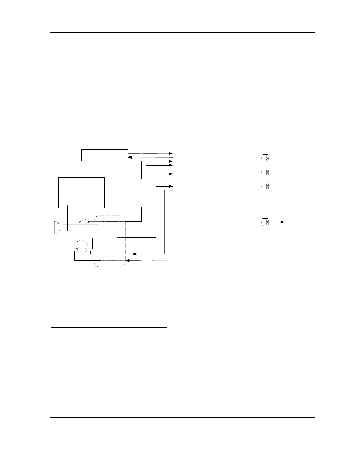
Figure 5.1. Connect the laptop computer (via 9-pin serial port connector), audio signal generator
using BNC coax cable, the pilot headset, and transmitter key using the Headset/Serial Interface
Harness as shown in Figure 5.2. Apply 28V DC power to UUT. Boot the laptop computer, and
double-click the “VHF_Display” icon. Check for the flashing green light on the display showing
Fig 5.1 - View of UUT hardware.
Table 5.1 – List of required support equipment, and adapters.
Vendor/ Part # Description
David Clark Pilot headset
Avidyne Headset/Serial Interface Harness
Audio Spectrum Audio signal generator
Avidyne Power Cable (Banana jacks to 5x12 60-pin connector
“RS-232 Active”. If not active enter “dbg1” in the Command window. If it is not necessary to type
“dbg1” that means the debug switch on the serial interface harness is in the “debug” position, which
is usually undesirable since it will override audio ALC among other things. So unless needed,
toggle the switch in the other direction, cycle power and reboot the unit.
Confidential property of Avidyne Corporation 610-00060Not to be disclosed without permission Revision: -00 Date:6/13/2006
Page 17 of 21
Page 18
DVX-740/750 VHF Nav/Com Functional Test Procedure
It is unnecessary to vary the receiver frequencies during emissions testing since all tuning,
downconverting and channel selectivity filtering is performed digitally after the analog signal has
been digitized (i.e. no LO, oscillator or clock frequencies change to retune the receivers). For
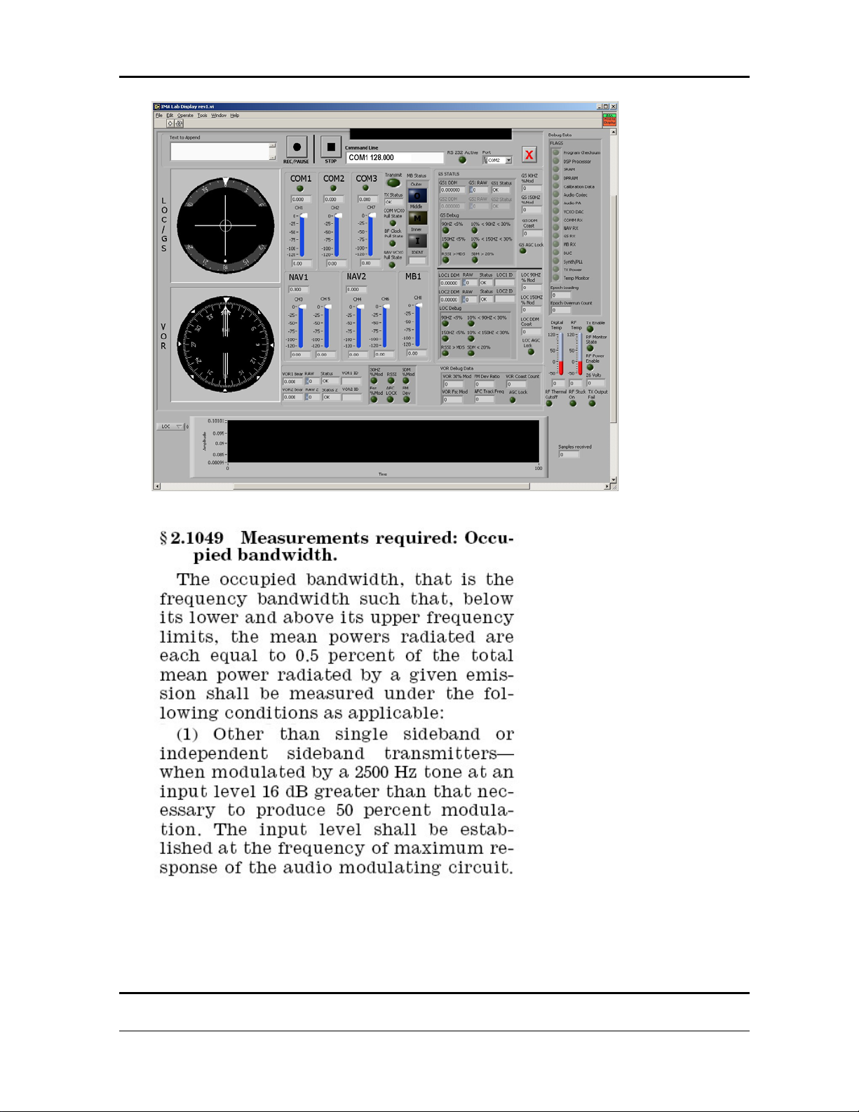
transmission, tune the COM1 operating frequency by entering a text string “COM1 XXX.xxx” in the
Command window of VHF Display as shown in Figure 5.4. Note that the program requires entry of
frequency in MHz, including 3 decimal places. Verify the frequency change in the COM1 frequency
window. Power-on default frequency is 118.200 MHz. Radio may now be keyed using the pushbutton hand key, and it will transmit a nominal 16W carrier if no audio input is applied. The
transmitted signal will be AM modulated by any audio signal presented on the audio input (poweron default input selection is Mic 1). 50% modulation is achieved with about 60mVrms input, and
automatic level control (ALC) will scale down audio inputs with peak excursions greater than about
90mVrms, to produce a nominal 70% AM modulation.
15 TX
14 RX
5 TX KEY 1
11 MIC 1 IN
21 AGND
26 AGND
28 AGND
25 AGND
44 HP 1
43 HP 3
HP Return
Left (Pilot)Radio
Comm Output to
Test Equipment
Audio
Analyzer
Chan A Out
Handheld PTT
Laptop
Pilot Audio Panel
Pilot HH PTT
Pilot HH Mic
Com 1
HP R
HP L
Pilot HH Mic Return
Notes: Shields are grounded only at the radio connector only.
Phone and mic jacks must be floating from ground.
Handheld
Headphones
Pilot HP R
Pilot HP L
Fig 5.2 - Test Configuration
Test 1 : RF Power Output Verification:
Set frequency at 118.000, 127.500, and 136.900 and measure carrier power at each frequency.
Modulate with 300mV audio input signal and measure mean output power.
Test 2 : Modulation Characteristics:
Set audio output level at 50-100 mV RMS and key the transmitter using the handheld key.
Observe power and modulation readings on a Modulation Analyzer. Adjust audio generator signal
level as necessary for the desired modulation level, or disable audio output for carrier only.
Test 3 : Occupied Bandwidth:
Set frequency at 118.000, 127.500, and 136.900 and measure carrier power at each frequency.
Modulate the carrier with a 300mV audio input signal and analyze the spectral content at each
frequency. Find the bandwidth beyond which all emissions are below -23dBc, which gives the
bandwidth containing 99.5% of the transmitter power, also known as the Occupied Bandwidth as
defined in the following excerpt from CFR47 Part2, paragraph 2.1049.
Confidential property of Avidyne Corporation 610-00060Not to be disclosed without permission Revision: -00 Date:6/13/2006
Page 18 of 21
Page 19
DVX-740/750 VHF Nav/Com Functional Test Procedure
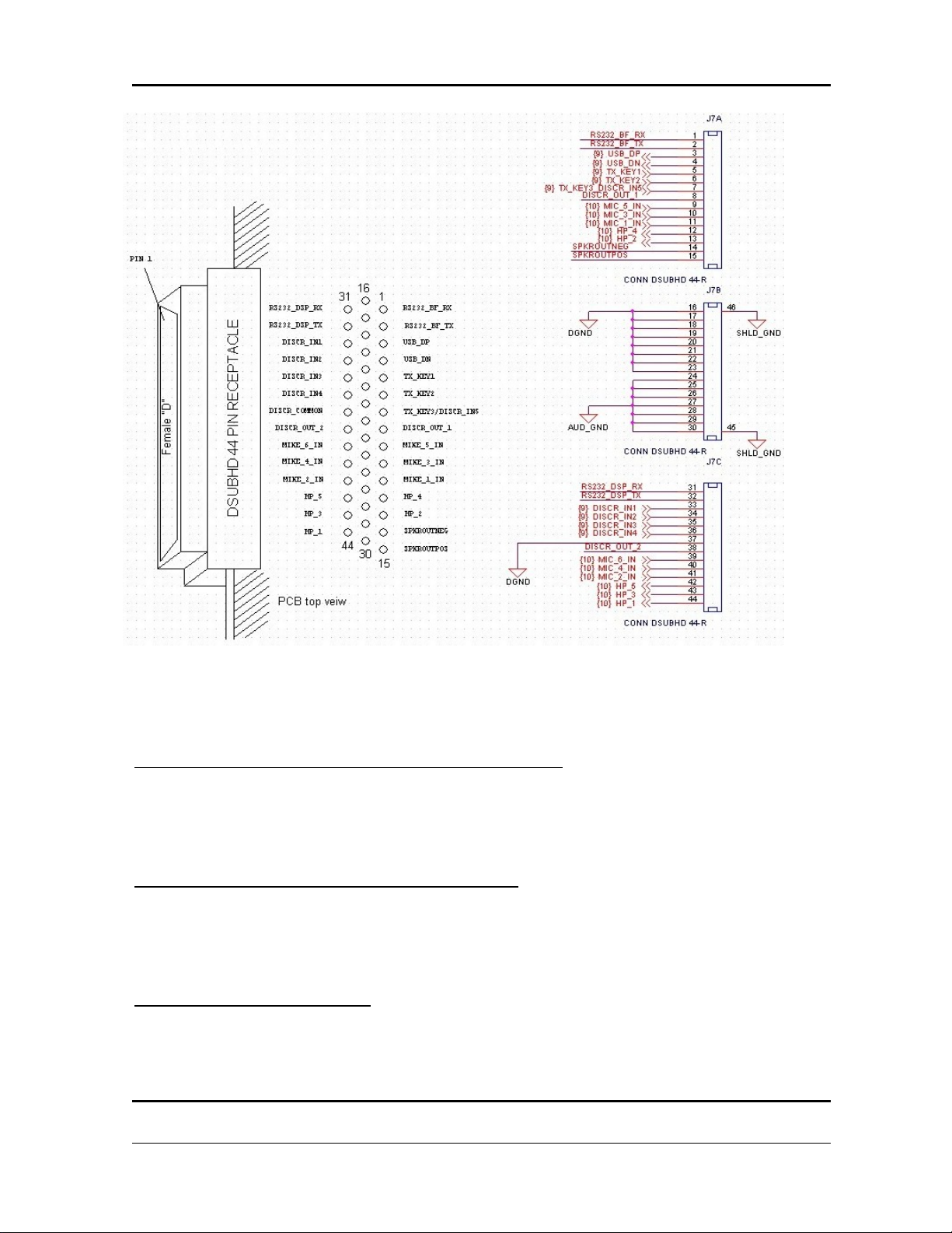
Figure 5.3 – Pin assignment for the 44-pin high density sub-D connector, J7.
The Headset/Serial Interface Harness connects external equipment and devices to the audio
I/O, transmitter key and serial data pins as required by Figure 5.3.
Test 4 : Spurious Emissions at Antenna Terminals
Operate the transmitter into an inline attenuator and spectrum analyzer, using carrier frequencies
of 118.000, 127.500 and 136.900 MHz while analyzing the transmitted output from 0Hz to 10GHz.
All spurious emissions (i.e. beyond 250% of the operating bandwidth) should not exceed limits
specified in CFR 47, Part 87, para 87.139.
Test 5 : Field Strength of Spurious Radiation
Operate the transmitter into a 50ohm 25W (or greater) dummy load at 118.000, 127.500 and
136.900 MHz. Analyzing the radiated emissions from the UUT from 0Hz to 10GHz at various
directions in azimuth and elevation. All spurious emissions (i.e. beyond 250% of the operating
bandwidth) should not exceed limits specified in CFR 47, Part 15, para 15.209
Test 6 : Frequency Stability
Operate the transmitter into an inline attenuator and spectrum analyzer, using carrier frequencies
of 118.000, 127.500 and 136.900 MHz and no audio modulation. Measure the output frequency to
ensure accuracy better than 30ppm as specified in CFR 47, Part 87, para 87.133.
Confidential property of Avidyne Corporation 610-00060Not to be disclosed without permission Revision: -00 Date:6/13/2006
Page 19 of 21
Page 20
DVX-740/750 VHF Nav/Com Functional Test Procedure
Fig 5.4 - Software Control interface.
Figure 5.5 – Definition of Occupied Bandwidth given in CFR47 Part2, paragraph 2.1049
The DVX-750 module is now ready for integration into its host chassis. After installation in host
chassis the FCC ID label shown in Figure 5.6 must be affixed to the outside of the unit. Preferrable
below the single BNC connector at the bottom of the rear panel.
Confidential property of Avidyne Corporation 610-00060Not to be disclosed without permission Revision: -00 Date:6/13/2006
Page 20 of 21
Page 21

DVX-740/750 VHF Nav/Com Functional Test Procedure
6. Glossary
AM – amplitude modulation
ADC – analog-to-digital converter device
AGC – automatic gain control
A-to-D – analog-to-digital conversion, or digitization
CODEC – coder/decoder simultaneously digitizes audio frequency inputs or converts digital
inputs to analog outputs, usually for multiple inputs and outputs.
DAC – digital-to-analog conversion device
DDC – digital downconverter (software controlled receiver)
LC – inductor-capacitor circuit
LNA – low-noise amplifier, usually the first amplifier in a radio signal receiver
LOC – Localizer – transmits signal to indicate whether approach is right or left of center
PA – power amplifier, usually referring to a radio transmitter circuit
PFD – Primary Flight Display
PIN – A semiconductor structure using P and N-type materials with an intrinsic layer
between them to alter the properties of the PN junction (P-Intrinsic-N)
SAW – surface acoustic wave device
T/R – transmit or receive switch connects either the receiver or the transmitter to a single
antenna.
TCXO – temperature compensated crystal oscillator
VCXO – voltage controlled crystal oscillator (frequency variation: <1000ppm)
VOR – VHF Omni-Range beacon, ground-based navigational beacon
XO – crystal oscillator, with no voltage control or temperature compensation
Confidential property of Avidyne Corporation 610-00060Not to be disclosed without permission Revision: -00 Date:6/13/2006
Page 21 of 21
 Loading...